Bhushan B. Handbook of Micro/Nano Tribology, Second Edition
Подождите немного. Документ загружается.


© 1999 by CRC Press LLC
Kulkarni, A.V. and Bhushan, B. (1996b), “Nano/Picoindentation Measurements on Single-Crystal Alu-
minum Using Modified Atomic Force Microscopy,”
Mater. Lett.
29
,
221–227.
Kulkarni, A.V. and Bhushan, B. (1997), “Nanoindentation Measurements of Amorphous-Carbon Coat-
ings,”
J. Mater. Res.,
12, 2707–2714.
LaFontaine, W.R., Yost, B., Black, R.D., and Li, C.Y. (1990), “Indentation Load Relaxation Experiments
with Indentation Depth in the Submicron Range,”
J. Mater. Res.
5, 2100–2106.
Li, W.B., Henshall, J.L., Hooper, R.M., and Easterling, K.E. (1991), “The Mechanism of Indentation
Creep,”
Acta Metall. Mater.
39, 3099–3110.
Majumder, A., Oden, P.I., Carrejo, J.P., Nagahara, L.A., Graham, J.J., and Alexander, J. (1992), “Nanom-
eter-Scale Lithography Using the Atomic Force Microscope”,
Appl. Phys. Lett.
61, 2293–2295.
Miyamoto, T., Kaneko, R., and Miyake, S. (1991), “Tribological Characteristics of Amorphous Carbon
Films Investigated by Point Contact Microscopy,”
J. Vac. Sci. Technol. B
9, 1338–1339.
Page, T.F., Oliver, W.C., and McHargue, C.J. (1992), “The Deformation Behavior of Ceramic Crystals
Subjected to Very Low Load (Nano) Indentations,”
J. Mater. Res.
7, 450–473.
Parkinson, B. (1990), “Layer-by-Layer Nanometer Scale Etching of Two-Dimensional Substrates Using
the Scanning Tunneling Microscopy,”
J. Am. Chem. Soc.
112, 7498–7502.
Pethica, J.N., Hutchings, R., and Oliver, W.C. (1983), “Hardness Measurements at Penetration Depths as
Small as 20 nm,”
Philos. Mag.
A 48, 598–606.
Pharr, G.M. (1992), “The Anomalous Behavior of Silicon During Nanoindentation,” in
Thin Films: Stresses
and Mechanical Properties,
III (W.D. Nix, J.C. Braveman, E. Arzt, and L.B. Freund, eds.),
Vol. 239,
pp. 301–312, MRS, Pittsburgh.
Pharr, G.M., Oliver, W.C., and Clarke, D.R. (1989), “Hysteresis and Discontinuity in the Indentation
Load-Displacement Behavior of Silicon,”
Scrip. Metall.
23, 1949–1952.
Pharr, G.M., Oliver, W.C., and Clarke, D.R. (1990), “The Mechanical Behavior of Silicon during Small-
Scale Indentation,”
J. Electr. Mater.
19, 881–887.
Silver, R.M., Ehrichs, E.E., and deLozanne, A.L. (1987), “Direct Writing of Submicron Metallic Features
with a Resonance,”
Phys. Rev. Lett.
70, 3506–3509.
Tsau, L., Wang, D., and Wang, K. L. (1994), “Nanometer Scale Patterning of Silicon(100) Surface by an
Atomic Force Microscope Operative in Air,”
Appl. Phys. Lett.
64, 2133–2135.
Utsugi, Y. (1990), “Nanometer-Scale Chemical Modification Using a Scanning Tunneling Microscope,”
Nature
347, 747–749.

Bhushan, B. “Boundary Lubrication Studies Using Atomic Force/Friction ...”
Handbook of Micro/Nanotribology.
Ed. Bharat Bhushan
Boca Raton: CRC Press LLC, 1999
© 1999 by CRC Press LLC

© 1999 by CRC Press LLC
8
Boundary Lubrication
Studies Using Atomic
Force/Friction
Force Microscopy
Bharat Bhushan
8.1 Introduction
8.2 Nanodeformation, Adhesive Forces, and Molecular
Conformation
8.3 Boundary Lubrication Studies
Liquid Lubricants • LB and Self-Assembled Monolayers
8.4 Closure
References
8.1 Introduction
Boundary films are formed by physical adsorption, chemical adsorption, and chemical reaction. The
physisorbed film can be either monomolecular or polymolecular thick. The chemisorbed films are
monomolecular, but stoichiometric films formed by chemical reaction can have a large film thickness.
In general, the stability and durability of surface films decrease in the following order: chemical reaction
films, chemisorbed films, and physisorbed films. A good boundary lubricant should have a high degree
of interaction between its molecules and the sliding surface. As a general rule, liquids are good lubricants
when they are polar and thus able to grip solid surfaces (or be adsorbed). Polar lubricants contain reactive
functional groups with low ionization potential or groups having high polarizability (Bhushan, 1993).
Boundary lubrication properties of lubricants are also dependent upon the molecular conformation and
lubricant spreading (Novotny et al., 1989; Novotny, 1990; Mate and Novotny, 1991; Mate, 1992a).
This chapter presents an overview of lubrication studies of polar and nonpolar lubricants and Lang-
muir–Blodgett and chemically grafted films, using atomic force/friction force microscopy.
8.2 Nanodeformation, Adhesive Forces,
and Molecular Conformation
Nanodeformation behavior of the bonded lubricant was studied using atomic force microscopy (AFM)
by Blackman et al. (1990a). They used Si(100) substrate with about 1.5 nm of native oxide. Just prior to
© 1999 by CRC Press LLC
the application of lubricant, the surface was cleaned with methylene chloride, spun dried, and followed
by exposure to ultraviolet-created ozone for several minutes to remove the remaining adsorbates. Liquid
films of the perfluoropolyether Z-Dol of about 4-nm thickness were deposited by a dip-coating method.
The lubricant molecules were bonded to the substrate via the reactive end groups by heating at 150°C
for 1 h, followed by rinsing with a freon solvent to remove any unbonded molecules, leaving behind
about 2-nm-thick film. Before bringing a tungsten tip into contact with a molecular overlayer, it was
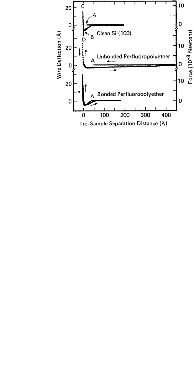
first brought into contact with a bare clean-silicon surface, Figure 8.1. As the sample approaches the tip,
the force initially is zero, but at point A the force suddenly becomes attractive (top curve) which increases
until at point B where the sample and tip come into intimate contact and the force becomes repulsive.
As the sample is retracted, a pull-off force of 5
×
10
–8
N (point D) is required to overcome adhesion
between the tungsten tip and the silicon surface. The deformation is reversible (elastic) since the retracting
(outgoing) portion of the curve (C to D) follows the extending (ingoing) portion. When an AFM tip is
brought into contact with a molecularly thin film of a nonreactive lubricant, a sudden jump into adhesive
contact is observed. The adhesion is initiated by the formation of a lubricant meniscus surrounding the
tip pulling the surfaces together by Laplace pressure. However, when the tip was brought into contact
with a lubricant film which was firmly bonded to the surface, the liquidlike behavior disappears. The
initial attractive force (point A) is no longer sudden as with the liquid film, but, rather, gradually increases
as the tip penetrates the film. Meniscus formation is suppressed because the polymer molecules are no
longer free to move about on the surface as at least one end is attached.
According to Blackman et al. (1990a), if the substrate and tip were infinitely hard with no compliance
in the tip and sample supports, the line for B to C would be vertical with an infinite slope. The tangent
to the force–distance curve at a given point is referred to as the stiffness at that point and was determined
by fitting a least-squares line through the nearby data points. For bonded lubricant film, at the point
where slope of the force changes gradually from attractive to repulsive, the stiffness changes gradually,
indicating compression of the molecular film. As the load is increased, the slope of the repulsive force
eventually approaches that of the bare surface. The bonded film was found to respond elastically up to
the highest loads of 5 µN which could be applied. Thus, bonded lubricant behaves as a soft polymer solid.
FIGURE 8.1
Wire deflection (normal load) as a function of tip–sample separation distance curves comparing the
behavior of clean Si(100) surface to a surface lubricated with free and unbonded PFPE lubricant, and a surface where
the PFPE lubricant film was thermally bonded to the surface. (From Blackman, G. S. et al. (1990),
Phys. Rev. Lett.
65, 3189–3198. With permission.)
© 1999 by CRC Press LLC
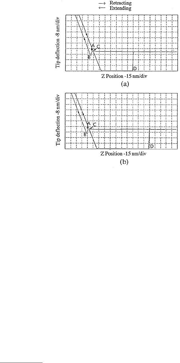
The attractive adhesive forces at different parts of the surface can be estimated by bringing the sample
into contact with the tip and then measuring the maximum force needed to pull the tip and sample
apart, Mate (1993) and Bhushan and Ruan (1994). Figure 8.2 shows typical normal load as a function
of separation distance (
Z
) curves for unlubricated and lubricated (with about 2-nm thickness of a
perfluoropolyether lubricant with an alcohol group, Z-Dol) magnetic disk samples. In these experiments,
the disks are first brought into contact and then withdrawn from the tip. The presence of the water vapor
for the unlubricated disk and along with the lubricant film for the lubricated disk causes a sudden
attractive force to occur at point A due to a meniscus of liquid forming around the top of the liquid film
and a long break-free distance out to point B where the liquid meniscus breaks as the sample is withdrawn.
The major difference between the two curves is that the pull-off force is lower for the unlubricated surface
compared with lubricated surface. Pull-off force is determined by multiplying the cantilever spring
constant (0.4 N/m) by the horizontal distance between points C and D, which corresponds to the
maximum cantilever deflection toward the disks before the tip is disengaged. The horizontal distance/pull-
off force is 105 nm/42 nN for the unlubricated disk and 160 nm/64 nN for the lubricated disk. The higher
value of the pull-off force in the case of lubricated disk arises from the larger meniscus contribution from
the liquid films (Bhushan and Ruan, 1994).
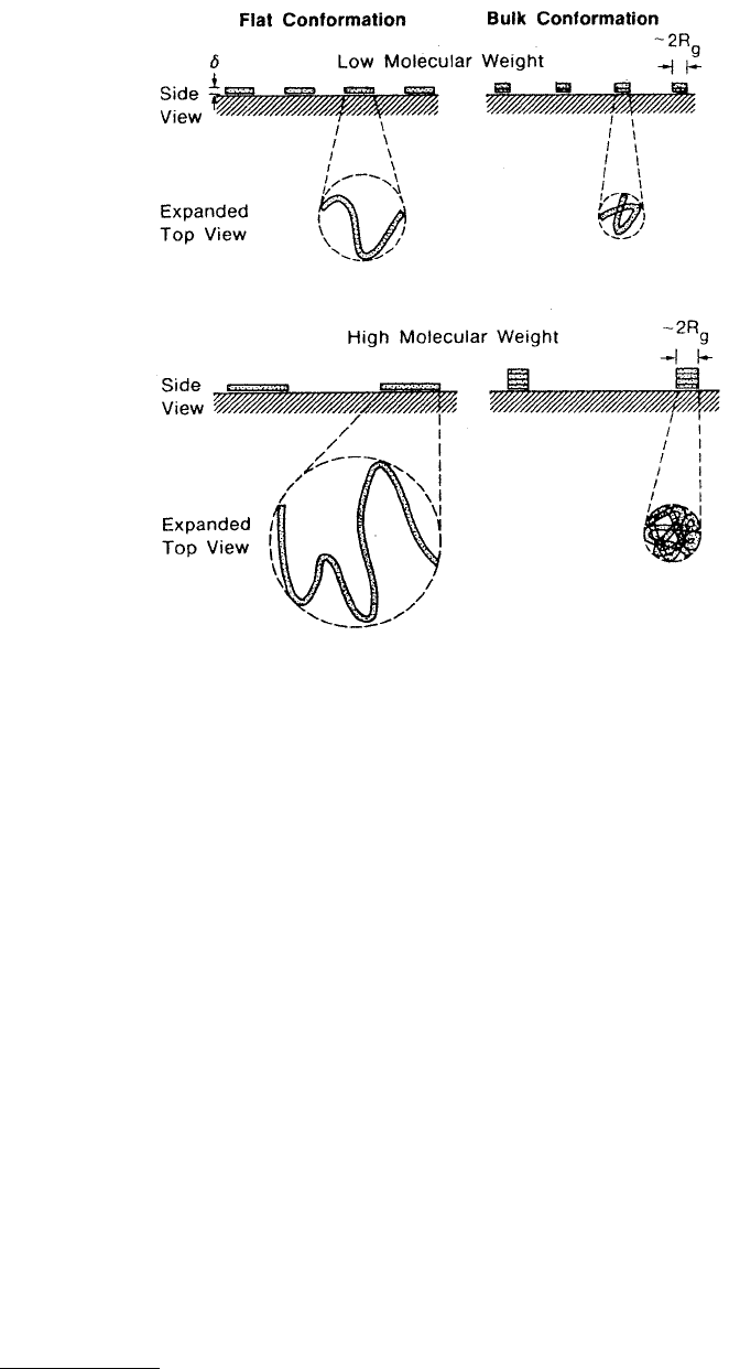
Figure 8.3 illustrates two extremes for the conformation on a surface of a linear liquid polymer without
any reactive end groups and at submonolayer coverages (Novotny et al., 1989; Mate and Novotny, 1991).
At one extreme, the molecules lie flat on the surface, reaching no more than their chain diameter
δ
above
the surface. This would be the case if a strong attractive interaction exists between the molecules and the
FIGURE 8.2
Tip deflection (normal load) as a function of Z (separation distance) curve for (a) unlubricated and
(b) lubricated thin-film magnetic rigid disks. The pull-off force is 42 nN for the unlubricated disk and 64 nN for
the lubricated disk calculated from the horizontal distance between points C and D and the cantilever spring constant
of 0.4 N/m. (From Bhushan, B. and Ruan, J. (1994),
ASME J. Tribol.
116, 389–396. With permission.)
© 1999 by CRC Press LLC
solid. On the other extreme, when a weak attraction exists between polymer segments and the solid, the
molecules adopt conformation close to that of the molecules in the bulk, with the microscopic thickness
equal to about the radius of gyration
R
g
. Mate and Novotny (1991) used AFM to study conformation of
0.5- to 13-nm-thick perfluoropolyether molecules on clean Si(100) surfaces. They found that the thickness
measured by AFM is thicker than that measured by ellipsometry with the offset ranging from 3 to 5 nm.
They found that the offset was the same for very thin submonolayer coverages. If the coverage is
submonolayer and inadequate to make a liquid film, the relevant thickness is then the height (
h
e
)
molecules extended above the solid surface. The offset should then equal 2
h
e
, assuming that the molecules
extend the same height above both the tip and silicon surfaces. They thus concluded that the molecules
do not extend more than 1.5 to 2.5 nm above a solid or liquid surface, much smaller than the radius of
gyration of the lubricants ranging between 3.2 and 7.3 nm, and to the approximate cross-sectional
diameter of 0.6 to 0.7 nm for the linear polymer chain. Consequently, the height that the molecules
extend above the surface is considerably less than the diameter of gyration of the molecules and only a
few molecular diameters in height, implying that the physisorbed molecules on a solid surface have an
extended, flat conformation. They also determined the disjoining pressure of these liquid films from
AFM measurements of the distance needed to break the liquid meniscus that forms between the solid
surface and the AFM tip. (Also see Mate, 1992a). For a monolayer thickness of about 0.7 nm, the disjoining
pressure is about 5 MPa, indicating strong attractive interaction between the liquid molecules and the
solid surface. The disjoining pressure decreases with increasing film thickness in a manner consistent
with a strong attractive van der Waals interaction between the liquid molecules and the solid surface.
FIGURE 8.3
Schematic representation of two extreme liquid conformations at the surface of the solid for low and
high molecular weights at low surface coverage.
δ
is the cross-sectional diameter of the liquid chain and
R
g
is the
radius of gyration of the molecules in the bulk. (From Mate, C. M. and Novotny, V. J. (1991),
J. Chem. Phys.
92,
3189–3196. With permission.)
© 1999 by CRC Press LLC
Attempts to measure mechanical properties of self-assembled monolayer films on Au(111) films have
been made by Salmeron et al. (1993). They have used AFM in the tapping mode. This technique has the
potential of measuring local viscoelastic properties of lubricant films.
8.3 Boundary Lubrication Studies
8.3.1 Liquid Lubricants
Mate (1992b), O’Shea et al. (1992), Bhushan et al. (1995a–c), and Koinkar and Bhushan (1996a,b) used
AFM to provide insight into how lubricants function at the molecular level. Mate (1992b) conducted
friction experiments on Si(100) surface lubricated with a lubricant with alcohol end group (Z-Dol). In
these experiments, the sample was moved rapidly back and forth in the
X
-direction at a velocity of 1 µm/s,
while the normal load on the tip was slowly increased to some maximum value, then decreased back to
zero by moving the sample in the
Z
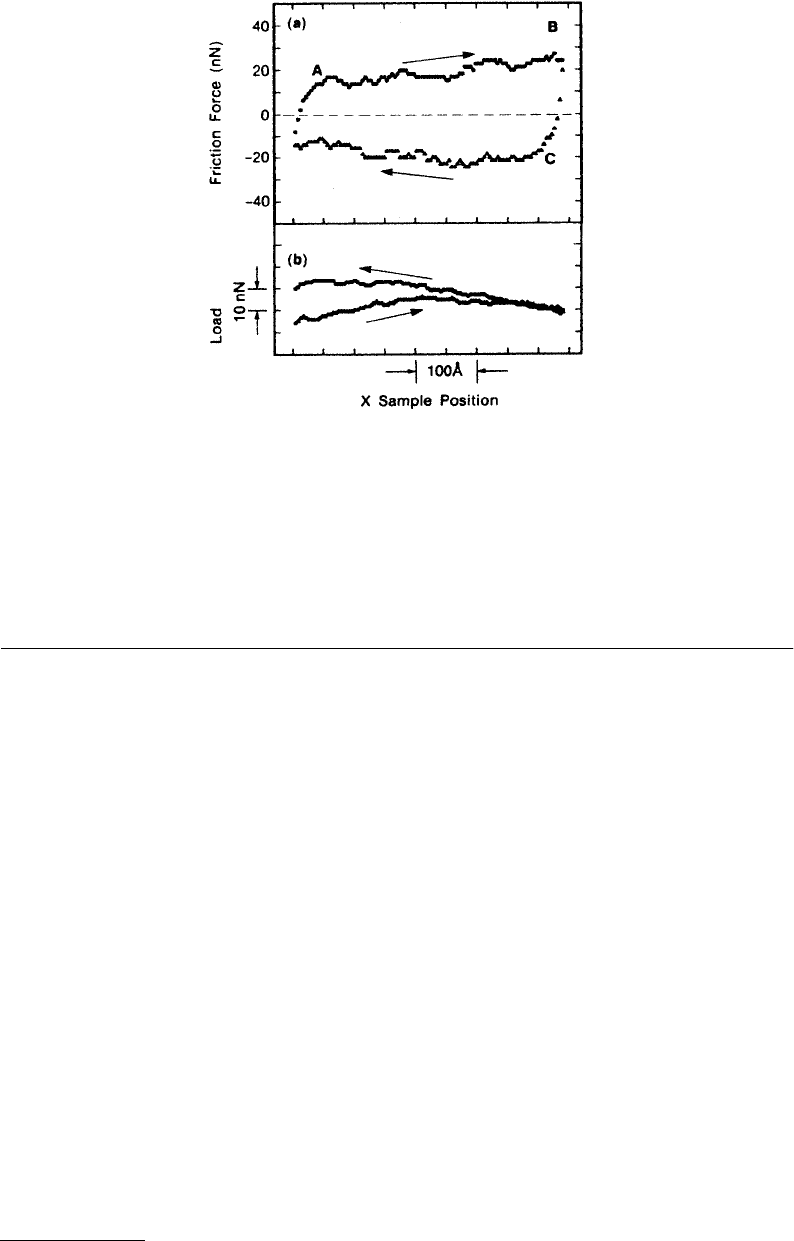
-direction. Figure 8.4 shows an example of the friction force on the
tip during one complete X oscillation of the sample. Initially, the tip moves with the sample, until, at
point A, the cantilever wire exerts enough force to overcome the static frictional force and the tip starts
to slide across the surface. When the X sample direction is reversed at point B, the tip again moves with
the sample until it starts to slide at point C. The upward shift in the normal load over the cycle comes
with the slight increase in load as the sample is slowly pushed up against the tip. The slight variation in
load during the cycle correspond to a surface roughness of about 0.1 nm.
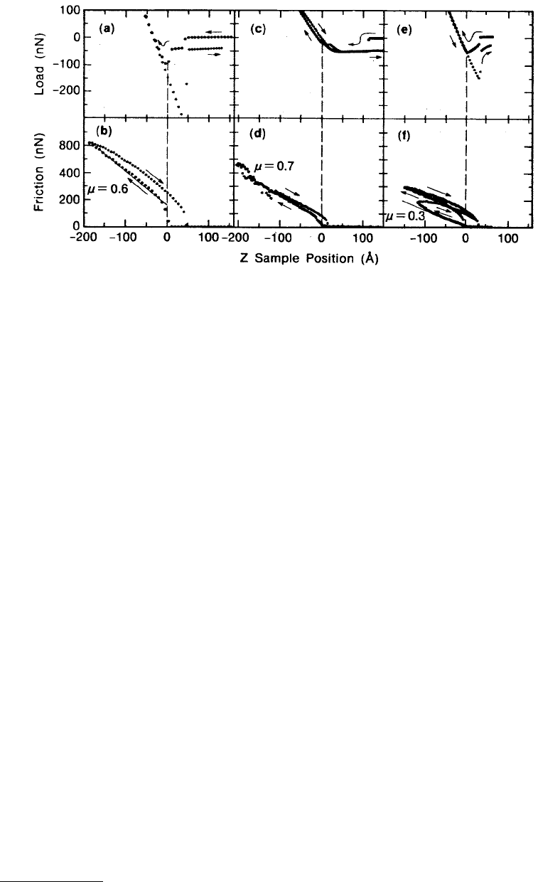
Figure 8.5 shows the average normal load and friction forces during sliding as a function of the
Z-sample position for the 3-nm-thick films of different types of lubricants. Each data point in the figure
represents the average over the sliding portion of a cycle in the X-direction like the one shown in
Figure 8.4. For the liquid film in Figure 8.5a and c, Mate (1992b) noted that, just before the hard wall
contact is made, the normal load during sliding becomes more attractive for nonalcohol end group (Z03)
than that for alcohol end group (Z-Dol) in the same manner as when no sliding occurs. When the sample
is withdrawn, the friction force returns to zero when the hard wall contact is broken. This regime is
called full-film lubrication, where shearing of a liquid film takes place resulting in a negligible friction
FIGURE 8.4
(a) Friction force and (b) normal load over an oscillation of the X-sample position during sliding of
the tungsten tip on an Si(100) surface coated with perfluoropolyether lubricant with alcohol end group. (From Mate,
C. M. (1992),
Phys. Rev. Lett.
68, 3323–3326. With permission.)
© 1999 by CRC Press LLC
(Bowdon and Tabor, 1950). After hard wall contact, one is in boundary lubrication regime, where
solid–solid shearing takes place. The transition between the two regimes is very sharp, requiring a change
in separation distance less than a chain diameter. In the boundary lubrication regime, the friction force
for the liquid films initially rises quickly, but soon increases linearly with load (coefficient of friction in
the range of 0.5 to 0.8). Similar values of the coefficient of friction are observed for unlubricated silicon
surfaces, indicating that most of the unbonded liquid lubricant is squeezed out from the rubbing surfaces.
Some liquid molecules may still be trapped among the microasperities of the tip and contribute to the
solid-solid shearing.
Figure 8.5e and f show the results from sliding on the bonded lubricant film prepared by conveniently
bonding of the alcohol-ended lubricant (by heating Z-Dol film at 150°C for 1 h in order to react the end
groups with hydroxyl groups on the silicon surface with native oxide and washing off nonreactive portion
with freon). As was the case for the unbonded lubricant, no significant friction is observed until the hard
wall contact was made. So, even though the ends of the polymer are rigidly attached to the substrate,
the backbone of the polymer apparently has enough flexibility to offer little resistance to the sliding tip
except when rigidly compressed between the two surfaces. For the bonded lubricant, the initial coefficient
of friction is about 0.3, which is about half that for the unbonded liquid films. The lower coefficient of
friction indicates that significantly more molecules are trapped between the rubbing surfaces than for
the unbonded lubricant. With repeated traversals of the sliding tip, these attached molecules eventually
wear away and the coefficient of friction increases with increasing load.
Mate (1992b) concluded that the liquid films have negligible shear stress to applied shear strains until
the molecules are completely compressed or squeezed out from between the sliding surfaces, showing
that hydrodynamic lubrication can occur for surfaces separated by only a few cross-sectional diameters
of the polymer backbone. (Also see O’Shea et al., 1992, 1994). The addition of alcohol end groups greatly
improves the resistance of the molecules to being squeezed out from between the sliding surfaces.
Koinkar and Bhushan (1996a,b) studied the friction and wear performance of Si(100) sample lubri-
cated with about 2-nm-thick Z-15 and Z-Dol perfluoropolyether (PFPE) lubricants. Z-Dol film was
thermally bonded at 150°C for 30 min and washed off with a solvent to provide a chemically bonded
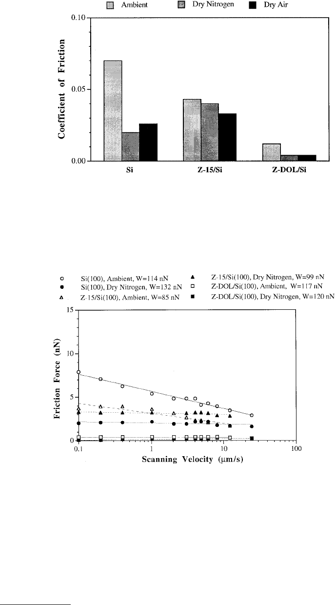
layer of the lubricant film. Data showing the effect of environment on the unlubricated and lubricated
samples are summarized in Figure 8.6. Note that lubricated silicon samples show a lower value of
FIGURE 8.5
The friction force and normal load as a function of the Z sample position for 3-nm-thick films on
Si(100) of (a), (b) unbonded lubricant with unreactive end groups, (c), (d) unbonded lubricant with alcohol end
groups and (e), (f) bonded lubricant. The open circles in (f) show the friction force when the experiment is repeated
in the same spot on the bonded lubricant. (From Mate, C. M. (1992),
Phys. Rev. Lett.
68, 3323–3326. With permission.)
© 1999 by CRC Press LLC
coefficient of friction than that of unlubricated sample. Furthermore, sample lubricated with Z-Dol
exhibits a lower value of the coefficient of friction than that of the Z-15 lubricated sample. For the
unlubricated and lubricated samples, the coefficient of friction in a dry environment is lower than at
ambient of about 50% relative himidity. At high humidity, the condensed water film from the environ-
ment results in dewetting of the lubricant film (or water film for the unlubricated sample) resulting in
poorer lubrication performance. Figure 8.7 shows the effect of scanning velocity on the coefficient of
FIGURE 8.6
Coefficient of friction for unlubricated and lubricated samples in ambient (~50% RH), dry nitrogen
(~5% RH), and dry air (~5% RH). (From Koinkar, V. N. and Bhushan, B. (1996),
J. Vac. Sci. Technol. A
14, 2378–2391.
With permission.)
FIGURE 8.7
Friction force as a function of scanning velocity for unlubricated and lubricated samples in ambient
and dry nitrogen environments. Normal loads used are given in the figure. (From Koinkar, V. N. and Bhushan, B.
(1996),
J. Vac. Sci. Technol. A
14, 2378–2391. With permission.)
© 1999 by CRC Press LLC
fricition in ambient and dry nitrogen environments. The coefficient of friction of unlubricated silicon
sample and lubricated with Z-15 decreases with an increase of the scanning velocity in the ambient
environment, whereas the sample lubricated with Z-15 in the dry nitrogen and the sample lubricated
with Z-Dol in both ambient and dry nitrogen environments do not show any velocity dependence. We
believe that alignment of free liquid molecules at higher scanning velocities results in lower values of the
coefficient of friction.
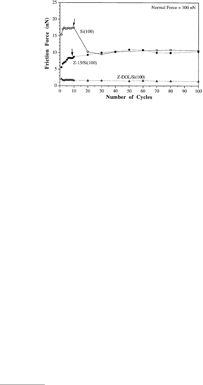
To study lubricant depletion during microscale measurements, Koinkar and Bhushan (1996a,b) con-
ducted nanowear studies using Si
3
N
4
tips. They measured friction as a function of the number of cycles
for virgin silicon and silicon surfaces lubricated with Z-15 and Z-Dol lubricants, Figure 8.8. An area of
1
×
1 µm was scanned at a normal force of 300 nN. Note that the friction force in a virgin silicon surface
decreases in a few cycles after the natural oxide film present on silicon surface gets removed. In the case
of Z-15-coated silicon sample, the friction force starts out to be low and then approaches that of an
unlubricated silicon surface after a few cycles. The increase in friction of the lubricated sample suggests
that the lubricant film gets worn and the silicon underneath is exposed. In the case of the Z-Dol-coated
silicon sample, the friction force starts out to be low and remains low during the 100-cycles test. It suggests
that Z-Dol does not get displaced/depleted as readily as Z-15. (Also see Bhushan et al., 1995a.) Microwear
studies were also conducted using the diamond tip at various loads. Figure 8.9 shows the plots of wear
depth as a function of normal force and Figure 8.10 shows the wear profiles of worn samples at 40 µN
normal force. The Z-Dol-lubricated sample exhibits better wear resistance than the unlubricated and
Z-15-lubricated silicon samples. Wear resistance of the Z-15-lubricated sample is little better than that
of the unlubricated sample. The Z-15-lubricated sample shows debris inside the wear track. Since Z-15
is a liquid lubricant, debris generated is held by the lubricant and it becomes sticky, which moves inside
the wear track and does damage, Figure 8.10.
8.3.2 LB and Self-Assembled Monolayers
Organized and dense molecular-scale layers of, preferably, long-chain molecules have shown to be
superior lubricants on both macro- and microscales as compared with freely supported multimolecular
layers (Bhushan et al., 1995b,c). Common methods to produce monolayers and thin films (Ulman, 1991)
are the Langmuir–Blodgett (LB) deposition (Roberts, 1990) and self-assembled films by chemical grafting
of molecules (Jaffrezic-Renault and Martelet, 1992). The LB films are bonded to the substrate by weak
FIGURE 8.8
Friction force as a function of number of cycles using an Si
3
N
4
tip at a normal load of 300 nN for
unlubricated and lubricated samples in ambient environment. Arrows in the figure indicate significant changes in
the friction force because of removal of surface or lubricant film. (From Koinkar, V. N. and Bhushan, B. (1996),
J. Vac. Sci. Technol. A
14, 2378–2391. With permission.)