Douglas H. Williams. PDA Robotics. 2003. 256p
Подождите немного. Документ загружается.


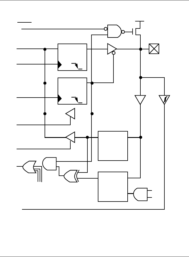
“mismatch” outputs of RB7:RB4 are ORed together to generate the RB
Port Change Interrupt with flag bit RBIF (INTCON<0>). This interrupt
can wake the device from SLEEP. The user, in the Interrupt Service
Routine, can clear the interrupt in the following manner:
• Any read or write of PORTB. This will end the mismatch condition.
• Clear flag bit RBIF.
PDA Robotics
88
WR Port
Data Bus
RBPU
(2)
I/O
pin
(1)
WR TRIS
RD TRIS
RD Port
RB0/INT
RB3/PGM
Data Latch
TRIS Latch
TTL
Input
Buffer
Weak
Pull-up
P
VDD
CK
Q
CK
QD
D
QD
EN
Note 1:
2:
I/O pins have diode protection to VDD and VSS.
To enable weak pull-ups, set the appropriate TRIS
bit(s) and clear the RBPU bit (OPTION_REG<7>).
RD Port
Schmitt Trigger
Buffer
Figure 5.35
Block diagram of RB3:RB0 pins.
PDA 05 5/30/03 11:35 AM Page 88
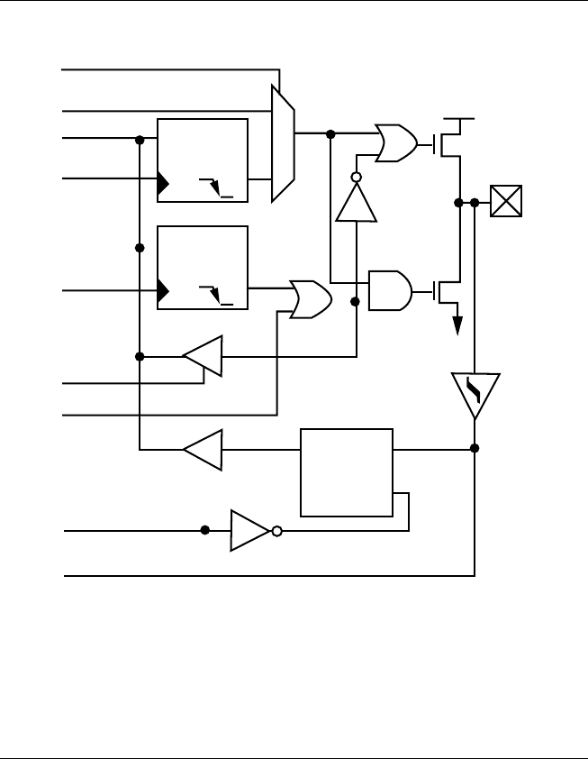
A mismatch condition will continue to set flag bit RBIF. Reading
PORTB will end the mismatch condition and allow flag bit RBIF to be
cleared. The interrupt-on-change feature is recommended for wake-up
on key depression operation and operations where PORTB is only
used for the interrupt-on-change feature. Polling of PORTB is not rec-
ommended while using the interrupt-on-change feature.
Chapter 5 / The Electronics
89
WR Port
Data Bus
RBPU
(2)
I/O
pin
(1)
WR TRIS
RD TRIS
RD Port
Set RBIF
Data Latch
TRIS Latch
TTL
Input
Buffer
Weak
Pull-up
P
V
DD
CK
Q
D
CK
QD
QD
EN
QD
EN
Note 1:
2:
I/O pins have diode protection to VDD and VSS.
To enable weak pull-ups, set the appropriate TRIS
bit(s) and clear the RBPU bit (OPTION_REG<7>).
From other
RB7:RB4 pins
Latch
ST
Buffer
Q1
Q3
RD Port
RB7:RB6
In Serial Programming Mode
Figure 5.36
Block diagram of RB7:RB4 pins.
PDA 05 5/30/03 11:35 AM Page 89

This interrupt-on-mismatch feature, together with software config-
urable pull-ups on these four pins, allows easy interface to a keypad
and make it possible for wake-up on key depression.
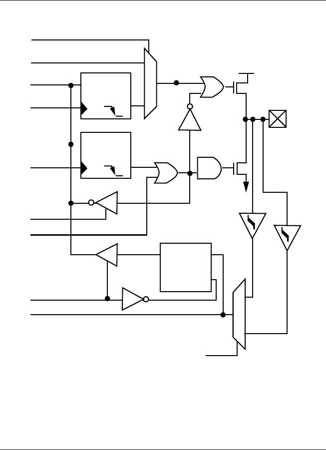
PORTC and the TRISC Register
PORTC is an 8-bit-wide, bidirectional port. The corresponding data
direction register is TRISC. Setting a TRISC bit (= 1) will make the cor-
responding PORTC pin an input (i.e., put the corresponding output
driver in a Hi-Impedance mode). Clearing a TRISC bit (⫽ 0) will make
the corresponding PORTC pin an output (i.e., put the contents of the
output latch on the selected pin).
PORTC is multiplexed with several peripheral functions. PORTC pins
have Schmitt Trigger input buffers. When the I2C module is enabled,
the PORTC<4:3> pins can be configured with normal I2C levels, or
with SMBus levels by using the CKE bit (SSPSTAT<6>). When enabling
peripheral functions, care should be taken in defining TRIS bits for
each PORTC pin. Some peripherals override the TRIS bit to make a pin
an output, while other peripherals override the TRIS bit to make a pin
an input. Since the TRIS bit override is in effect while the peripheral is
enabled, read modify write instructions (BSF, BCF, XORWF) with
TRISC as destination, should be avoided. The user should refer to the
corresponding peripheral section for the correct TRIS bit settings.
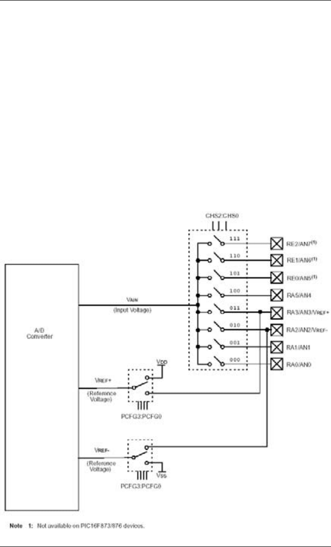
Analog-to-Digital Converter (A/D) Module. The Analog-to-Digital
(A/D) Converter module has five inputs for the 28-pin devices and
eight for the other devices. The analog input charges a sample and
hold capacitor. The output of the sample and hold capacitor is the
input into the converter. The converter then generates a digital result
of this analog level via successive approximation. The A/D conversion
of the analog input signal results in a corresponding 10-bit digital
number. The A/D module has high- and low-voltage reference input
that is software selectable to some combination of VDD, VSS, RA2, or
RA3. The A/D converter has a unique feature of being able to operate
while the device is in SLEEP mode. To operate in SLEEP, the A/D
clock must be derived from the A/D’s internal RC oscillator.
The A/D module has four registers. These registers are:
• A/D Result High Register (ADRESH)
PDA Robotics
90
PDA 05 5/30/03 11:35 AM Page 90
• A/D Result Low Register (ADRESL)
• A/D Control Register0 (ADCON0)
• A/D Control Register1 (ADCON1)
The ADCON0 register controls the operation of the A/D module. The
ADCON1 register configures the functions of the port pins. The port
Chapter 5 / The Electronics
91
Port/Peripheral Select
(2)
Peripheral
OE
(3)
Peripheral Data Out
Data Bus
WR
Port
WR
TRIS
RD
TRIS
RD
Port
Peripheral input
I/O
pin
(1)
Data Latch
TRIS Latch
Schmitt
Trigger
P
N
V
DD
VSS
CK
Q
Q
D
CK
Q
Q
D
QD
EN
Note 1:
2:
I/O pins have diode protection to VDD and VSS.
Port/Peripheral select signal selects between port
data and peripheral output.
3:
Peripheral OE (output enable) is only activated if
peripheral select is active.
0
1
Figure 5.37
PORTC block diagram (peripheral output override) RC<2.0>, RC<7:5>.
PDA 05 5/30/03 11:35 AM Page 91
pins can be configured as analog inputs (RA3 can also be the voltage
reference), or as digital I/O. Additional information on using the A/D
module can be found in the PICmicro Mid-Range MCU Family
Reference Manual (DS33023).
Follow these steps when doing an A/D conversion:
PDA Robotics
92
Port/Peripheral Select
(2)
Peripheral
OE
(3)
Peripheral Data Out
Data Bus
WR
Port
WR
TRIS
RD
TRIS
RD
Port
SSPI Input
I/O
pin
(1)
Data Latch
TRIS Latch
Schmitt
Trigger
P
N
V
DD
VSS
CK
Q
Q
D
CK
Q
Q
D
QD
EN
Note 1:
2:
I/O pins have diode protection to VDD and VSS.
Port/Peripheral select signal selects between port
data and peripheral output.
3:
Peripheral OE (output enable) is only activated if
peripheral select is active.
0
1
0
1
Schmitt
Trigger
with
SMBus
levels
CKE
SSPSTAT<6>
Figure 5.38
PORTC block diagram (peripheral output override) RC<4:3>.
PDA 05 5/30/03 11:35 AM Page 92
1. Configure the A/D module:
• Configure analog pins/voltage reference and digital I/O
(ADCON1).
• Select A/D input channel (ADCON0).
• Select A/D conversion clock (ADCON0).
• Turn on A/D module (ADCON0).
2. Configure A/D interrupt (if desired):
• Clear ADIF bit.
• Set ADIE bit.
Chapter 5 / The Electronics
93
Figure 5.39
A/D block diagram.
PDA 05 5/30/03 11:35 AM Page 93

• Set PEIE bit.
• Set GIE bit.
3. Wait for the required acquisition time.
4. Start conversion:
• Set GO/DONE bit (ADCON0).
5. Wait for A/D conversion to complete, by either:
• Polling for the GO/DONE bit to be cleared (with interrupts
enabled); or
• Waiting for the A/D interrupt.
6. Read A/D result register pair (ADRESH:ADRESL); clear bit ADIF
if required.
7. For the next conversion, go to step 1 or step 2, as required. The
A/D conversion time per bit is defined as TAD. A minimum wait
of 2TAD is required before the next acquisition starts.
Once again, the C compiler we are using in this project takes care of
the preceding steps in a few simple lines of code!
Timer0 Module. The Timer0 module timer/counter has the follow-
ing features:
• 8-bit timer/counter
• Readable and writable
• 8-bit software programmable prescaler
• Internal or external clock select
• Interrupt on overflow from FFh to 00h
• Edge select for external clock
Figure 5.40 is a block diagram of the Timer0 module and the prescaler
shared with the WDT.
Timer mode is selected by clearing bit T0CS (OPTION_REG<5>). In
Timer mode, the Timer0 module will increment every instruction cycle
(without prescaler). If the TMR0 register is written, the increment is
PDA Robotics
94
PDA 05 5/30/03 11:35 AM Page 94
inhibited for the following two instruction cycles. The user can work
around this by writing an adjusted value to the TMR0 register.
Counter mode is selected by setting bit T0CS (OPTION_REG<5>). In
Counter mode, Timer0 will increment on either every rising or every
falling edge of pin RA4/T0CKI. The incrementing edge is determined
by the Timer0 Source Edge Select bit, T0SE (OPTION_REG<4>).
Clearing bit T0SE selects the rising edge.
The prescaler is mutually exclusively shared between the Timer0
module and the WDT. The prescaler is not readable or writable.
Timer0 Interrupt. The TMR0 interrupt is generated when the TMR0
register overflows from FFh to 00h. This overflow sets bit T0IF (INT-
CON<2>). The interrupt can be masked by clearing bit T0IE (INT-
CON<5>). Bit T0IF must be cleared in software by the Timer0 module
Interrupt Service Routine before re-enabling this interrupt. The TMR0
interrupt cannot awaken the processor from SLEEP, since the timer is
shut-off during SLEEP.
Chapter 5 / The Electronics
95
CLKOUT (= osc/4)
RA4/TOCKI
pin
TOSE
TOCS
Watchdog
Timer
0
0
0
0
1
1
1
1
M
U
X
M
U
X
Prescaler
PSA
PSA
PSA
WDT Enable bit
8
WDT
Time-out
PS2:PS0
8-bit Prescaler
8- - to 1-MUX
MUX
Data Bus
8
Set Flag Bit T0IF
on Overflow
Sync
2
Cycles
TMR0 Reg
Note: TOCS, TOSE, PSA, PS2:PS0 are (OPTION_REG<5:0>.
M
U
X
Figure 5.40
Block diagram of the Timer0/WDT prescaler.
PDA 05 5/30/03 11:35 AM Page 95

Using Timer0 with an External Clock. When no prescaler is used,
the external clock input is the same as the prescaler output. The syn-
chronization of T0CKI with the internal phase clocks is accomplished
by sampling the prescaler output on the Q2 and Q4 cycles of the inter-
nal phase clocks. Therefore, it is necessary for T0CKI to be high for at
least 2Tosc (and a small RC delay of 20 ns) and low for at least 2Tosc
(and a small RC delay of 20 ns).
Prescaler. There is only one prescaler available, which is mutually
exclusively shared between the Timer0 module and the WDT. A
prescaler assignment for the Timer0 module means that there is no
prescaler for the WDT, and vice versa. This prescaler is not readable or
writable (see Figure 5.39).
The PSA and PS2:PS0 bits (OPTION_REG<3:0>) determine the
prescaler assignment and prescale ratio. When assigned to the Timer0
module, all instructions writing to the TMR0 register (e.g., CLRF 1,
MOVWF 1, BSF 1, etc.) will clear the prescaler. When assigned to
WDT, a CLRWDT instruction will clear the prescaler along with the
WDT. The prescaler is not readable or writable.
Note: Writing to TMR0, when the prescaler is assigned to Timer0,
will clear the prescaler count, but will not change the prescaler
assignment.
The L298 Dual Full-Bridge Driver
(PDA Robot Motor Controller)
• Operating supply voltage up to 46 V
• Total DC current up to 4 A
• Low saturation voltage
• Over temperature protection
• Logical ”0” Input voltage up to 1.5 V (high noise immunity)
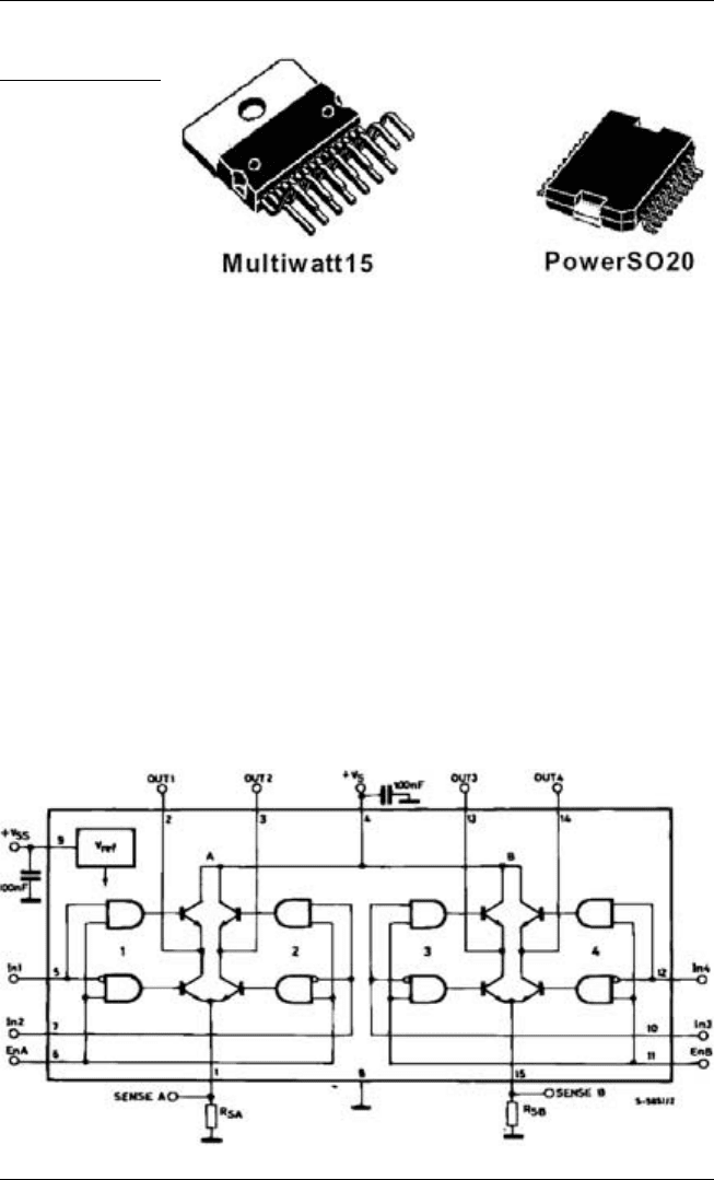
Figure 5.41 shows two of the three available packages that the L298
comes in. In this project, we are using the vertical package shown on
the left.
PDA Robotics
96
PDA 05 5/30/03 11:35 AM Page 96
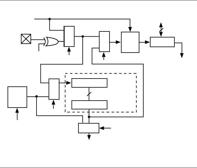
Description
The L298 is an integrated monolithic circuit in 15-lead Multiwatt and
PowerSO20 packages. It is a high-voltage, high-current, dual full-bridge
driver designed to accept standard TTL logic levels and drive inductive
loads such as relays, solenoids, DC, and stepping motors. Two enable
inputs are provided to enable or disable the device independently of
the input signals. The emitters of the lower transistors of each bridge
are connected together, and the corresponding external terminal can be
used for the connection of an external sensing resistor.
An additional supply input is provided so that the logic works at a
lower voltage, as is the case in PDA Robot. The logic supply comes
from the 5 V regulator on the main board via the ribbon connector and
the power supply, which drives the motors directly from the 6 V bat-
Chapter 5 / The Electronics
97
Figure 5.41
L298 packages.
Figure 5.42
L298 block diagram.
PDA 05 5/30/03 11:35 AM Page 97