Douglas H. Williams. PDA Robotics. 2003. 256p
Подождите немного. Документ загружается.

• Plastic development tray
• Rubber gloves
• Instruction sheet
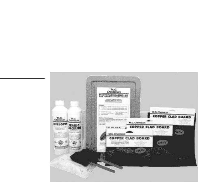
Figure 6.1 shows everything that is included in the kit.
Positive Photofabrication Process Instructions
Setup. Protect surrounding areas from developer and etchant splash-
es. Plastic is ideal for this. Work under safe light conditions. A 40 W
incandescent bulb works well. Important: Do not work under fluores-
cent light. If you do so, you will expose the board, making it unusable.
Just prior to exposure, remove white protective film from the presen-
sitized board. Peel it back carefully.
Exposing Your Board. For best results, use M.G. Chemicals cat.
#416-X exposure kit; however, any inexpensive lamp fixture that will
hold two or more 18" fluorescent tubes is suitable.
Place the presensitized board with the copper side toward the expo-
sure source. Lay positive film artwork onto the presensitized copper
side of the board and position as desired. Place the artwork printed
side down to prevent light leakage through the side of the transparen-
cy. Artwork should have been produced by a 600 dpi or better printer.
PDA Robotics
108
Figure 6.1
Contents of the
Photofabrication Kit
416-K.
PDA 06 5/27/03 8:37 AM Page 108
Use a glass weight to cover the artwork, ensuring that no light will
pass under traces (approx. 3 mm glass thickness or greater works best).
Use a 10-minute exposure time at a distance of 5".
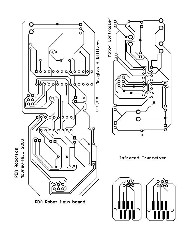
The artwork in Figure 6.3 needs to be reproduced on a transparency and
placed on the presensitized “green” surface of the circuit board. To do
this, either scan the artwork and print, make a high-quality photocopy,
or download the file from www.pda-robotics.com and print using a
photo editor. From the printer options, set the quality to its highest pos-
sible setting. I recommend checking the leads on the components to
ensure that the drill holes are the correct size and every hole lines up.
Important: You must print the image at 100%. If your printer settings
are not correct, the components will not fit. Watch out for the compo-
nents themselves. I found that the higher-priced components fit perfect-
ly, but with some of the less-expensive components, the pad and hole
sizes on the artwork may need to be enlarged or the leads filed or
crimped. This happened with the voltage regulators and L298 chips.
Variations from manufacturer to manufacturer will occur. To increase
the hole sizes, simply load the image into an image editor like
Paintbrush, and draw in white space after increasing the size of the pad.
Be careful when expanding the sizes. You don’t want any of the traces
to touch each other, and it’s good to leave as much space as possible.
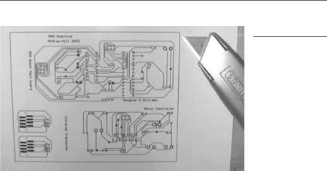
After printing the artwork on a good-quality transparency, cut it out
using a utility knife or scissors and put it on the presensitized side
after carefully peeling the protective cover off (see Figures 6.3 and
6.4).
Note: Ensure that the printing on the board in not reversed when plac-
ing on the presensitized side. The lettering “PDA Robotics” should be
shown as printed normally, not reversed.
Chapter 6 / Building PDA Robot
109
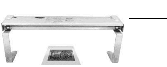
Figure 6.2
Fluorescent
exposure.
PDA 06 5/27/03 8:37 AM Page 109
Important: Be sure that no fluorescent lights are on anywhere nearby
when doing this. Place a clear glass or acrylic weight over the board
and transparency and place under the fluorescent light source. Expose
the board.
Developing Your Board. The development process removes any pho-
toresist that was exposed through the film positive to ultraviolet light.
Warning: Developer contains sodium hydroxide and is highly corro-
sive. Wear rubber gloves and eye protection while using it. Avoid con-
PDA Robotics
110
Figure 6.3
Artwork for the circuit board.
PDA 06 5/27/03 8:37 AM Page 110
tact with eyes and skin. Flush thoroughly with water for 15 minutes if
it is splashed in the eyes or on the skin.
Using rubber gloves and eye protection, dilute one part M.G. cat. #418
developer with 10 parts of tepid water (weaker is better than stronger)
in a plastic tray. Immerse the board copper side up into the developer,
and you will quickly see an image appear while you are lightly brush-
ing the resist with a foam brush. This should be completed within one
to two minutes. Immediately neutralize development action by rinsing
the board with water. The exposed resist must be removed from the
board as soon as possible. When you are done with the developing
stage, the only resist remaining will be covering what you want your
circuit to be. Completely remove the rest.
Note: Ensure that the mixture of water and developer is mixed thor-
oughly. If it is not, the traces may wash away when the board comes
in contact with a pocket of highly concentrated developer.
Etching Your Board. For best results, use the 416-E Professional
Etching Process Kit or 416-ES Economy Etching Kit. The most popu-
lar etchant is ferric chloride, M.G. cat. #415, an aqueous solution that
dissolves most metals. Use this solution undiluted, and be sure to
completely cover your board.
Warning: This solution is normally heated up during use, generating
unpleasant and caustic vapors. It is very important to have adequate
ventilation. Use only glass or plastic containers. Keep out of reach of
children. It may cause burns or stain. Avoid contact with skin, eyes,
Chapter 6 / Building PDA Robot
111
Figure 6.4
Cutting out the
circuit board
artwork.
PDA 06 5/27/03 8:37 AM Page 111

or clothing. Store in a plastic container. Wear eye protection and rub-
ber gloves.
Directions: If you use ferric chloride cold, it will take a long time to
etch the board. To speed up etching, heat the solution. A simple way
of doing this is to immerse the ferric chloride bottle or jug in hot water,
adding or changing the water to keep it hot. A thermostat-controlled
crock pot is also an effective way to heat ferric chloride, as are ther-
mostatically controlled submersible heaters—glass-enclosed such as
an aquarium heater. An ideal etching temperature is 50°C (120°F). Be
careful not to overheat it. The absolute maximum working tempera-
ture is approximately 57°C (135°F). The warmer the etch solution, the
faster the boards will etch. Ferric chloride solution can be used over
and over again, until it becomes saturated with copper. As the solution
becomes more saturated, the etching time will increase. Agitation
assists in removing unwanted copper faster. This can be accomplished
by using air bubbles from two aquarium air wands with an aquarium
air pump. Do not use aquarium “air stone.”
The etching process can be assisted by brushing the unwanted resist
with a foam brush while the board is submerged in the ferric chloride.
I found that rocking the board back and forth in the pan by holding it
by the edges with rubber gloves on works well. The ferric chloride can
be kept warm by placing the glass basin on a stove element set to low.
Turn on the fume hood to expel any fumes.
After the etching process is completed, wash the board thoroughly
under running water. Do not remove the remaining resist protecting
your circuit or image. It protects the copper from oxidation.
PDA Robotics
112
Figure 6.5
Circuit board ready
for etching.
PDA 06 5/27/03 8:37 AM Page 112
Removal of resist is not necessary when soldering components to the
board. By leaving the resist on, you protect the circuit from oxidation.
Tin plating the board is not necessary. In soldering, the heat disinte-
grates the resist underneath the solder, resulting in an excellent bond.
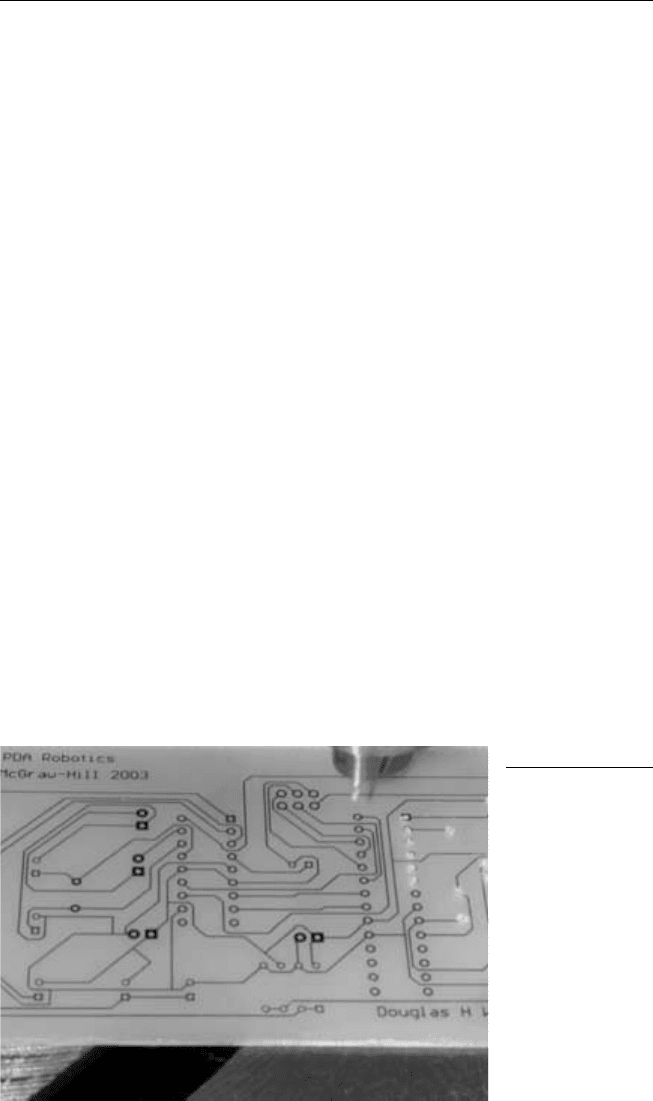
Drilling Out the Circuit Board. Once the board is dry, drill out the
holes using the appropriate drill bits. Be sure that the bit is in straight
and that you hit the hole dead center. Figure 6.6 shows the main board
being drilled out. Figure 6.7 shows the ribbon connector holes on a
transponder circuit board.
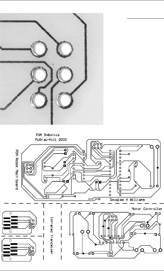
Cutting the Board. The board can be cut into the three sections by
repeatedly scoring with a utility knife, using a hacksaw, or using a
band saw. Note: Only one of the infrared (IR) transceiver boards is
required for this project. Figure 6.8 shows where the board should
be cut.
Placing and Soldering the Components. The boards are now ready
to have the components soldered into place. The components go onto
the topside of the board (opposite side from the traces), with the
exception of the TFDS4500 on the transceiver circuit board.
Chapter 6 / Building PDA Robot
113
Figure 6.6
Drilling the main
board.
PDA 06 5/27/03 8:37 AM Page 113
PDA Robotics
114
Figure 6.8
Cut the boards on the dotted lines.
Figure 6.7
Dead center drill.
PDA 06 5/27/03 8:37 AM Page 114

Parts Lists
The Main Board. Parts for the main board include:
• One PIC16F876 microcontroller
• One 28-pin DIP IC socket (or 2 18-pin DIP IC sockets with one cut
down)
• One MCP2150 IrDA protocol chip
• One 18-pin DIP IC socket
• One L7805ACV voltage regulator
• One 8-pin DIP switch
• One 11.0592 MHz crystal
• One 20.0000 MHz crystal
• One 3.9 mm (.156") Molex wire connectors
• One Molex 3.9 mm 2P header with ramp connects
• Two 6-post 2.5 mm DIP headers
• Two IDC6F DIP connector with key
• One Red LED
• Three 1 K resistor
• Two 47R 1/4 W resistors
• One 4.7 UF tantalum capacitor
• Six 22 pF capacitors
• One 1-pin
• 8" of six-wire ribbon cable
The Motor Controller. Parts for the motor controller include:
• One L298N dual bridge driver
• Four 3.9 mm (.156") Molex wire connectors
• Four Molex 3.9 mm 2P header with ramp connects
• Two 6-post 2.5 mm DIP headers
Chapter 6 / Building PDA Robot
115
PDA 06 5/27/03 8:37 AM Page 115

• Two IDC6F DIP connector with key
• Eight 4007 746 diodes
• Three .1 UF capacitors (or higher)
The IR Transceiver. Parts for the IR transceiver include:
• One TFDS4500
• One 6-post 2.5 mm DIP headers
• One IDC6F DIP connector with key
• 6" of six-wire ribbon cable
Range Finder and Attachments. Parts for the range finder and
attachments include:
• One GP2D12 distance measuring system with cable and attach-
ments (AIRRS @ www.hvwtech.com )
• Two .156" wire connectors
The Body. Parts for the body include:
• Aluminum: 8" ⫻ 6" ⫻ 1/16" (main platform)
• Aluminum: 7" ⫻ 5 1/4" (top platform) ⫻ 1/16"
• Aluminum: 1" ⫻ 1/2" ⫻ 1/4" (accessory mount)
• Two Tamiya six-speed geared motors (www.hvwtech.com)
• Three Tamiya wheel sets
• Four 1" L-brackets
• Five 2" 4-40 hex spacers
• Eight 1/2" 4-40 hex spacers
• One 9 V battery connector
• One 6 V battery pack (4 ⫻ 1.5 V AA)
• 6" of Velcro with self-basting adhesive (secure batteries)
• 1' of double-sided Velcro (secure PDA)
• Package of 50 4-40 1/4" nuts, bolts, and washers.
PDA Robotics
116
PDA 06 5/27/03 8:37 AM Page 116
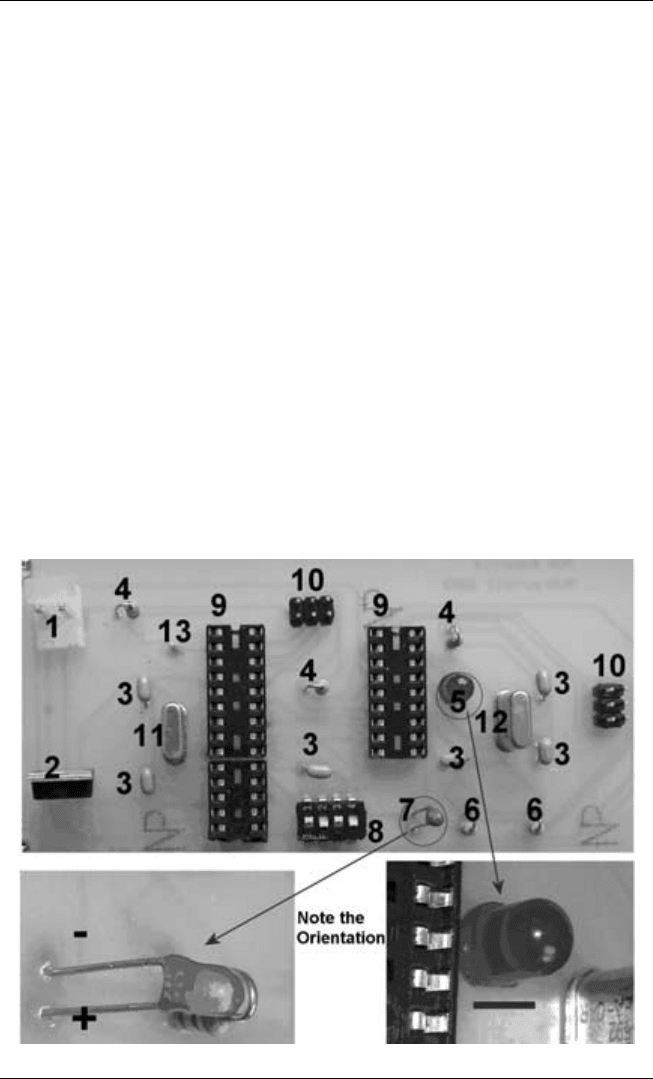
Placing and Soldering the
Main Board Components
Figures 6.9 to 6.11 show the placement of the parts. The following
numbers correspond to those on the main circuit board. Place and sol-
der the parts.
1. Molex 3.9 mm 2P header with ramp connects to Molex 156" (3.9
mm) wire connector
2. L7805ACV voltage regulator
3. 22 pF capacitors
4. 1 K resistors
5. Red LED
6. 47R 1/4 W resistors
7. 4.7 UF tantalum capacitor
Chapter 6 / Building PDA Robot
117
Figure 6.9
Main board par ts placement.
PDA 06 5/27/03 8:37 AM Page 117