Fahlman B.D. Materials Chemistry
Подождите немного. Документ загружается.


Figure 4.39. The steps involved in fabricating a CMOS IC. Reproduced with permission from Plummer,
J. D.; Deal, M. D.; Griffin, P. B. Silicon VLSI Technology, Prentice-Hall: New York, 2000.
278 4 Semiconductors

Figure 4.39. Continued
4.2. Silicon-Based Applications 279

A chlorine containing co-reactant gas such as HCl or trichloroethylene (H(Cl)
C ¼ CCl
2
) is often present during Si oxidation to increase the kinetics of silicon
oxidation. The reaction of oxygen with chlorinated species at elevated temperatures
results in chlorine formation (Eqs. 10 and 11). Chlorine has been shown to concen-
trate within 20 nm of the Si/SiO
2
interface thus expanding the oxide latt ice via
formation of a chlorosiloxane intermediate phase, which allows for faster diffusion
of the oxidant.
[24]
The oxidation rate is also enhanced by larger concentrations of n-
and p- dopants. That is, during high-temperature oxidation, dopant atoms may
migrate into the interfacial region (Table 4.1), weakening the Si-O bonding and
enhancing the dif fusivity of the oxidizing species through the oxide layer. It is also
likely that the direct reaction of Si with chlorine results in the formation of volatile
silicon chlorides, which yields interfacial vacancies. This will also cause an increase
in the oxidation rate, since either more Si atoms will diffuse into the vacant sites of
the interfacial region or mor e oxygen is entrapped at the surface.
4 HCl þO
2
, 2H
2
O þ 2Cl
2
ð10Þ
4C
2
HCl
3
þ9O
2
! 2H
2
O þ 6Cl
2
þ 8CO
2
ð11Þ
It has been shown that small amounts (<5%) of chlorine in the gas phase helps to tie
up sodium or potassium ions that may be present as contaminants, removing metallic
impurities by forming volatile by-products, as well as strengthening the growing
oxide film by preventing oxidation-induced stacking faults.
[25]
During oxidation,
0.1% of the Si atoms at the Si/SiO
2
interface will not be incorporated into the
growing oxide lattice & will instead diffuse back into interstitial sites of the Si
lattice. If the growth rate is sufficiently high (esp. at T > 950
C), the interstitial
Si atoms do not equilibrate with vacan cies, thus condensing as extrinsic stacking
faults lying on [111] planes. Interestingly, these stacking faults may be repaired via
enhanced atomic diffusion by post-annealing the wafer at a temperature greater than
1,200
C under an inert atmosphere.
Following oxidation, it has been shown that 0.001% of the silicon atoms in the
region immediately surrounding the Si/SiO
2
interface remain unsaturated. This is
likely an artifact of incomplete oxidation during the transition from Si to SiO
2
.
The presence of these defects results in a layer of positive charge that is located
within 2 nm from the interface. These trapped charges will induce a charge of
opposite polarity in the underlying Si, which will affect the V
T
of the MOSFET and
performance of the IC as a whole. Although thes e effects are minimized by using
Table 4.1. Dopant Diffusion Constants in SiO
2
at 1,100
C
Dopant atom Diffusion constant (cm
2
/s)
B 3.4 10
17
2.0 10
14
Ga 5.3 10
11
P 2.9 10
16
2.0 10
13
As 1.2 10
16
3.5 10
15
Sb 9.9 10
17
280 4 Semiconductors

Si(100) substrates,
[26]
additional processing steps also address this issue; for
instance, passivation through low-temperature (ca. 450
C) annealing in the presence
of hydrogen.
Also shown in step (a) of Figure 4.39 is the deposition of silicon nitride, Si
3
N
4
over the SiO
2
layer. The nitride film is generated through a high-temp erature
reaction betwee n ammonia and silane gases (Eq. 12). The thicknesses of the SiO
2
and Si
3
N
4
films are typically on the order of 15 and 75 nm, respectively. Since the
density of silicon nitride is sufficiently greater than SiO
2
(3.3 g cm
3
vs. 2.6 g cm
3
,
respectively), Si
3
N
4
is used as an effective passivating layer to prevent oxidation of
underlying SiO
2
and Si regions.
3 SiH
4
+4NH
3
!
800
c
Si
3
N
4
þ12 H
2
ð12Þ
Patterning via photolithography
The surface patterning steps of IC fabrication are based on photolithogr aphy
[27]
(Figure 4.40), which accounts for 90% of the overall production cost. In this
procedure, a photosensitive compound known as a photoresist is first spin-coated
onto the surface of the wafer. Frequently, the wafer is pretreated by a dehydration
SiO
2
Si(100)
Photoresist
SiO
2
Si(100)
Mask
Photoresist
i) wet etch with 6:1 NH
4
F:HF
OR
ii) dry etch with anhydrous HF at 150-190 ⬚C (0.1 - 30 Torr)
iii) remove photoresist using an O
2
plasma
i) Development
ii) Hard bake
(ca. 120 ⬚C for 30 min)
Spin-coating
i) Soft bake (ca. 90 ⬚C for 30 min)
ii) Mask alignment
UV light
Figure 4.40. Schematic of photolithography and the chemical (“wet”) and “dry” methods used to etch
patterns in an oxidized Si wafer.
4.2. Silicon-Based Applications 281

bake (to remove adsorbed water) and application of an adhesion promotor (e.g.,
hexamethyl disilazane, HMDS – Figur e 4.41; others include trichlorophenylsilane
(C
6
H
5
SiCl
3
) and bis(trimethylsilyl)acetamide ((CH
3
)
3
SiNCH
3
COSi(CH
3
)
3
) for Si
substrates
[28]
). These “primers” chemically bond to the Si substrate, thereby gen-
erating a polar electrostatic surface that will more efficiently bond the photo resist.
In order to achieve the best possible line resolution, the photoresist should possess
the following requirements:
(i) High sensitivity (results in less exposure time and lower cost)
(ii) High contrast (only brightly illuminated areas will be chemically changed)
(iii) Strong surface adhesion
(iv) Resistance to etching conditions
A circuit pattern of the microscopic IC known as a mask
[29]
is placed over the
wafer, and the uncovered molecules of the photoresist that are exposed to high-
energy UV light will exhibit a chemical change (Figure 4.42). Negative tone photo-
resists undergo photo-induced cross linking mechanisms upon UV exposure.
The ensui ng polymerization reaction is due to the presence of photosensitive groups
such as epoxy, vinyl, or aryl halides on the photoresist backbone. Accordingly, they
become insoluble during subsequent contact with a basic developing solution (e.g.,
MOH, tetramethyl ammonium hydroxide). In contrast, use of positive tone
HMDS
CH
3
CH
3
Si(CH
3
)
3
H
3
C
HN
OH
CH
3
NH
3
CH
3
H
2
N-Si(CH
3
)
3
H
2
N-Si(CH
3
)
3
+
H
3
CSi
O
CH
3
CH
3
H
3
C
Si
O
CH
3
CH
3
H
3
C
Si
O
Si
Figure 4.41. The reactions involved in the adhesion of HMDS to a SiO
2
surface. Attachment occurs
through available surface hydroxyl groups, with the release of ammonia.
282 4 Semiconductors

Figure 4.42. Molecular structures and photoinduced reactions of common photoresists. Shown are (a) the
diazonaphthoquinone (DNQ) positive tone photoresist, and (b) the SU-8 epoxy-based negative tone
photoresist.
4.2. Silicon-Based Applications 283

photoresists results in the exposed-polymer regions becoming preferentially soluble
in the developing solution. Although early photolithographic applications used
negative tone photoresists exclusively, the organic matrices of these materials
caused swelling, which results in pattern distortion during development. In order
to reproduce line features below 3 mm present in today’s electronic devi ces, aqueous
base-soluble positive photoresists are most commonly employed. However, aqueous
negative tone photoresists have now been developed with line resolut ions below
1 mm.
[30]
As one can see from Eq. 13, decreasing the wavelength of exposure for photoli-
thography will directly improve the resulting line resolution. Table 4.2 lists the
wavelengths and optimum resolution values for various lithographic techniques.
Since 2002, IC fabrication has used 193-nm UV irradiation (ArF source) for
patterning. Photolithography using 157-nm (F
2
laser source) was to be instituted a
few years later to further progress the rapid miniaturization of ICs; however, it was
deemed too costly. That is, in addition to switching from atmospheric-pressure to
high-vacuum environments, new photoresists and masks would also need to be
designed.
R=
0:61l
NA
ð13Þ
where R is the resolution limit (line spacing capable of being resolved – smaller R is
better) and NA is the numerical aperture of the exposure tool (the light-gathering
power of a lens – discussed in more detail in Chapter 7).
Though decreasing the exposure wavelength improves line resolution, issues
associated with absorption will become increasingly problematic. The use of
extreme UV light (EUV), within the range of soft X-rays (ca. l ¼ 13.4 nm;
100 eV), has also been developed for IC fabrication. This was once touted to soon
replace 193-nm photolithography (Figure 4.43); however, the use of phase-shift
masks (Figure 4.44) and double-/multiple-exposure techniques
[31]
has extended the
193-nm exposure far beyond the original predictions. The EUV source is based on a
plasma generated from an IR laser that impinges upon gas-phase Xe clusters
expanding at supersonic speeds. Rather than conventional lenses, EUV also dictates
Table 4.2. Resolution Limits for Various Lithographic Techniques
Lithographic technique Exposure wavelength (nm) Resolution
Photolithography
a
mid-UV (MUV) 350–450 0.35–3 mm
Photolithography deep-UV (DUV) 248 0.25 mm
Photolithography deep-UV (DUV) 193 <30 nm
b
Photolithography extreme-UV (EUV) 13.5 <20 nm
Electron-beam lithography
c
ca.1 <10 nm
X-ray lithography
d
0.4–20 <30 nm
a
Using a standard chrome-on-glass photomask.
b
Using advanced photomask techniques such as phase-shift masks (PSMs, Figure 4.32).
c
Using a photomask of Si
3
N
4
membrane and Cr/W patterned regions.
d
Using a photomask of Si/Si
3
N
4
/SiC/BN membrane and Au/W patterned regions.
284 4 Semiconductors
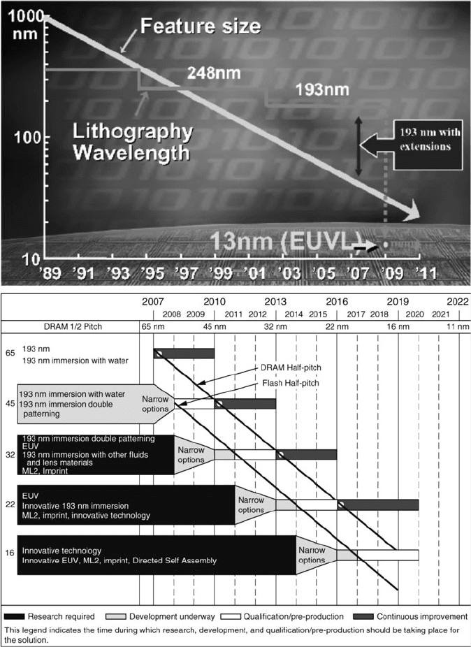
Figure 4.43. Top: The trend of shrinking feature size, which is outpacing the decrease in wavelength
currently used for photolithography. Reproduced with permission from Intel Corporation (http://www.
intel.com). Bottom: 2007 International Technology Roadmap for Semiconductors (ITRS), showing the
timeline for likely adoption of emerging lithographic technologies. Reproduced with permission from
Kumar, B. W. Extreme Ultraviolet Lithography, McGraw-Hill: New York, 2009. Copyright 2009
McGraw-Hill, Inc.
4.2. Silicon-Based Applications 285

the use of Si/Mo multilayered mirrors (Figure 4.45) to focus the plasma radiation
and reduce the size of the projected image from the mask.
[32]
A decrease in exposure wavelength translates to new types of photoresists
that will be stable upon contact with higher energy radiation. Whereas the DNQ
photoresist system is effective in the MUV range, photoresists that feature
chemical amplification (CAM) moieties are used exclusively for DUV and shorter
wavelengths.
[34]
The enhancement of quantum efficienc y and sensitivity results
Figure 4.44. The benefits of using phase-shift masks for photolithography. Reproduced with permission
from Plummer, J. D.; Deal, M. D.; Griffin, P. B. Silicon VLSI Technology, Prentice-Hall: New York, 2000.
Figure 4.45. Schematic of an Extreme UV (EUV) Mask.
[33]
286 4 Semiconductors
from a photogenerated acid that catalyzes either cross linking (negative
photoresists), or deprotection (positive photoresists) reactions. Since the diffusion
of acid during the post-exposure bake cycle sparks reactions with numerous func-
tional groups of the surrounding photoresist, fewer photons are required during UV
exposure. In order to facilitate water solubility, modern photoacid generators
(PAGs) are typically aryl sulfonium triflate salts (Figure 4.46). However, com-
pounds such as o-nitrobenzyl tosylate or organic/inorganic onium salts may also
be used as PAGs within organic solvents.
[35]
Within the wavelength regime of EUV, most materials exhibit very strong absorp-
tion; this is in contrast to X-ray lithography (exposure l of 0.8–1.4 nm), which is largely
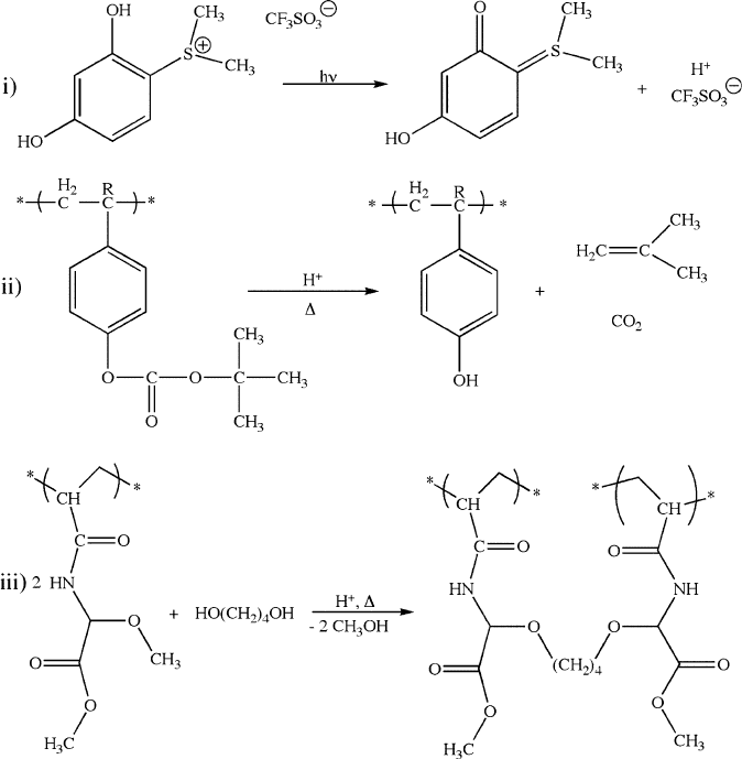
Figure 4.46. Chemical amplification (CAM). Reaction (i) represents photoinduced acid generation
(PAG); step (ii) is an acid-catalyzed deprotection mechanism (positive tone resist); and step (iii) is an
acid-catalyzed crosslinking mechanism (negative tone resist).
4.2. Silicon-Based Applications 287