Fahlman B.D. Materials Chemistry
Подождите немного. Документ загружается.

best candidates for CVD, as they are often less susceptible to premature hydrolysis
during transfer to the CVD system. Co-reactant gases such as NH
3
,H
2
,H
2
S, H
2
O, etc.
are often added in order to assist the removal of organic moieties from the organo-
metallic precursor molecule, preventing their incorporation in the growing film.
The use of mixed precursors adds complexity to the control over film stoichiometry.
The different volatilities of the precursors often lead to irreproducible vapor-phase
concentrations. As a result, flow rates have to be carefully controlled to give films of a
desired composition. Another problem that is posed by the use of mixed precursors is
the variable rate of hydrolysis/oxidation, resulting in morphologically varied films.
Hence, it is most preferable to use a precursor that contains as many desired building
blocks of the thin film as possible. For the films deposited during IC fabrication,
common precursors include silane (SiH
4
) with co-reactant gases of H
2
(for polysilicon
films), NH
3
(for Si
3
N
4
), and O
2
(for SiO
2
). For tungsten films, a 1:3 WF
6
:H
2
precursor
mixture is used; TiN is deposited using a TiCl
4
/NH
3
combination (Eq. 18):
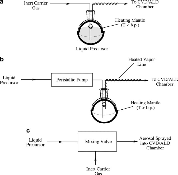
Figure 4.62. CVD/ALD delivery methods for liquid precursors. Shown are (a) carrier gas bubbling of a
volatile precursor, (b) vaporization of a volatile precursor, and c) direct liquid injection (DLI) of a volatile/
non-volatile precursor.
308 4 Semiconductors
6 TiCl
4
þ 8NH
3
!
500
c
6 TiN þ 24 HCl þ N
2
ð18Þ
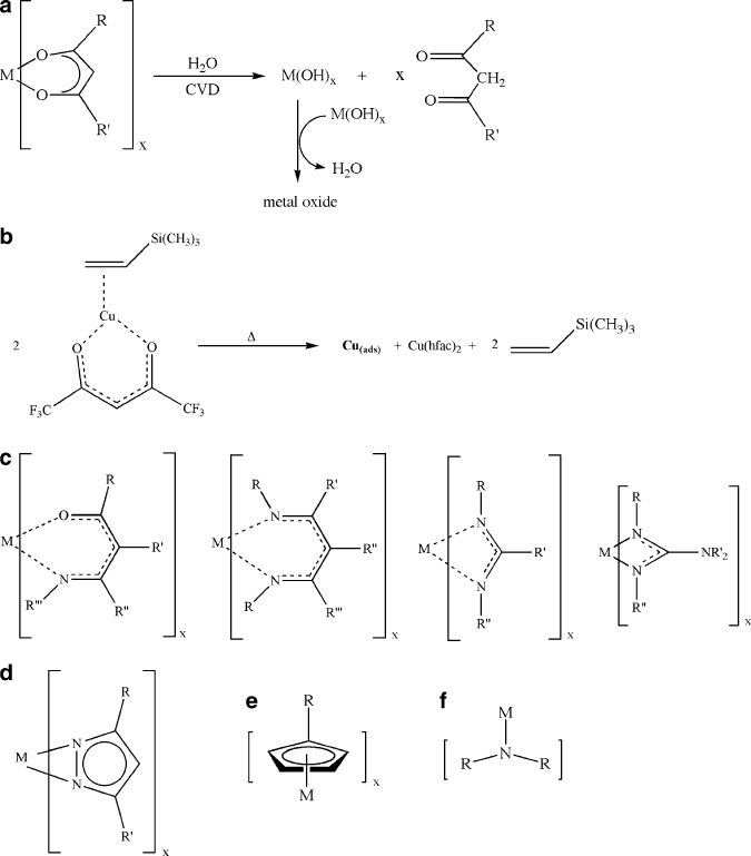
Figure 4.63 illustrates the chemical structures of a variety of precursors that
may be used for CVD/ALD applications.
[57]
Metal alkoxides (M(OR)
x
) and
Figure 4.63. Molecular structures of commonly used CVD precursor classes. Shown are: (a) metal
b-diketonate (acetylacetonate, acac) complex to grow a metal oxide film (H
2
as the coreactant gas
yields a metal film); (b) a heteroleptic (more than one type of ligand bound to the metal) b-diketonate
complex to yield a Cu film; the ancillary ligand helps prevent oligomerization, enhancing volatility;
(c) various types of complexes to deposit metallic, oxide, nitride, or oxynitride films (depending on
coreactant gas(es) used – respective ligands are b-ketoiminato, b-diketiminato, amidinato, and
guanidinato; (d) a metal azolato complex commonly used to deposit lanthanide metal films; metal
cyclopentadienyl (cp) complexes, (e), and dialkylamido complexes, (f), are often used to deposit a
variety of metallic or compound thin films.
4.2. Silicon-Based Applications 309
halides represent the earliest known examples; mixed metal alkoxide precursors
(e.g., for bimetallic thin film growth) may be synthesized by the following route
(A ¼ Group 1 metal):
M(ORÞ
x
þ AOR ! AM(ORÞ
xþ1
ð19Þ
y AM(ORÞ
xþ1
þ M
0
Cl
y
! M
0
½MðORÞ
xþ1
y
þ y AClð20Þ
Metal b-diketonate complexes have been used extensively to deposit thin films
of most metals and their oxides. Their low cost and high volatility make them
wise candidates for precursors; however, they generally result in large concentra-
tions of carbon incorporated into the film. Replacing one oxygen with -NR sub-
stituents results in the b-ketoiminato ligand system. The greater basicity of the
nitrogen-donor ligands relative to oxygen analogues has been reported to increase
the volatility through enhanced metal-ligand bonding.
[58]
Replacing both oxygen
groups with -NR moieties results in the b-diketiminato ligand, which provides
further thermal stability of the resultant metal comple x, while offering a tunable
volatility by varying the imine substituents.
The volatility of a precursor is related to its molecular weight (i.e., London
Dispersion intermolecular forces), as well as its degree of oligomerization. As
such, it is also common to have a metal complex that features bulky ligands
[59]
or
the use of an ancillary Lewis base (e.g., alkene, alkyne, triorganophosphine, vinyl-
silane, etc.) to prevent oligomerization. Such a complex with more than a single
type of ligand surrounding the central metal is known as a heteroleptic complex; in
contrast, homoleptic complexes have only a single ligand type, such as Al(C
2
H
5
)
3
.
Another effective method to enhance precursor volatility is to incorporate partially
and fully fluorinated ligands. The enhancement may be rationalized either by an
increased amount of intermolecular repulsion due to the additional lone pairs or that
the reduced polarizability of fluorine (relative to hydrogen) causes fluorinated
ligands to have less intermolecular attractive interactions.
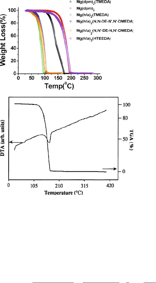
Prior to CVD studies, it is essential that the potential precursor undergo thermo
gravimetric analy sis (TGA) and differential scanning calorimetry (DSC) to deter-
mine the most suitable temperature regime for thin-film growth (Figure 4.64).
A sharp TGA curve with no remaining residue indicates that the precursor vaporizes
without significant ligand decomposition – most desirable for CVD applications.
Further, if the mass loss via TGA occurs concomitantly with a single endot herm
via DSC, then sublimation of the precursor is occurring without decomposition
(Figure 4.64, bottom) – ideal behavior for CVD applications.
In addition to simple mass-loss vs. T investigations, TGA may als o be applied to
accurately determine the enthalpy of sublimation (DH
sub
), as well as the sublimation
temperature (T
sub
) of a solid.
[60]
In these investigations, the mass loss through
sublimation (m
sub
) will be constant at a given temperature, as long as the phase
change occurs without appreciable decomposition. Hence, by measuring the mass
loss over a variety of isothermal regions, a plot of log(m
sub
T
1/2
) vs.1/T may be
310 4 Semiconductors
generated, which readily yields values of DH
sub
and T
sub
from the slope and
y-intercept, respective ly (Eq. 21):
log m
sub
ffiffiffi
T
p
¼
0:0522 DH
sub
ðÞ
T
þ
0:0522 DH
sub
ðÞ
T
sub
1
2
log
1306
M
w
ð21Þ
It is often desirable to deposit films that possess more complex stoichiometries.
These films may include mixed-metal, and binary/ternary metal oxides and sulfides
that are of importance for emerging applications for catalysis and microelectronics.
Figure 4.64. Top: Thermogravimetric analysis of organomagnesium CVD precursors, indicating the
dependence of molecular structure on its decomposition temperature. Bottom: Tandem TGA/DSC
analyses showing a single endothermic event (sublimation) that coincides with the mass loss. The
ligand abbreviations are: dpm ¼ 2,2,6,6-tetramethyl-3,5-heptanedionate, TMEDA ¼ N, N, N
0
, N
0
-
tetramethylethylenediamine, hfa ¼ 1,1,1,5,5,5-hexafluoro-2,4-pentanedione, HTEEDA ¼ H(N, N, N
0
,
N
0
-tetraethylethylene diamine). Reproduced with permission from Chem. Mater. 2005, 17(23), 5697.
Copyright 2005 American Chemical Society.
4.2. Silicon-Based Applications 311
Although these materia ls may be generated through use of individual species, such
as Y, Ba, and Cu b-diketonates for YBa
2
Cu
3
O
7d
superconductor films,
[61]
it is most
advantageous to use a single-source precursor for thes e applications. The fixed ratio
of component metals in the individual precursor molecules offers a unique route
toward stoichiometric control over thin-film and nanoparticulate growth. Further,
lower deposition or post-annealing temperatures are often required for single-source
precursors relative to their co-reactant analogs.
Perhaps the greatest “Achilles heel” of using single-source precursors is the
complex and expensive synthetic procedures that are often required. Although this
is usually overcome in laboratory-scale processes, this represents a major limitation
for industrial scale-up consi derations. Recently, a one-step reaction scheme was
designed to yield a host of single-source precursor molecules that were suitable
for the CVD growth of I–III–VI semiconductors (Figure 4.65).
[62]
Subsequent CVD
studies using the ternary sulfide precursors were performed using an aerosol delivery
methodology, with films of comparable purity to those generated by highly
expensive procedures such as PVD from co-evaporation of source metals.
Next-generation patterning: “soft” lithography
The design of transistors, with feature sizes currently much less than 100 nm, will
need to move beyond traditional photolithography in order to continue Moore’s
Law and the miniaturization of electronic devices. In addition to the exorbitant cost
of photolithography, this technique is not amenable for the patterning of large and
[{PPh
3
}
2
Ag(SMe)
2
In(SMe)
2
]
[{PPh
3
}
2
Ag(SMe)
2
In(SMe)
2
]
E = S, R = Et,
L = PPh
3
, M=Cu
E = Se, R = Ph,
L = PBu
3
, M=Cu
E = Se, R = Ph,
L = PPh
3
, M=Cu
E = S, R = Et,
L = PBu
3
, M=Cu
4NaER + InCl
3
+ MX + 2L
E = S, R = Et, L = PBu
3
, M=Ag
E=S, R=Me
L = PPh
3
, M=Ag
E = S, R = Me, L = PPh
3
, M = Cu
[{PPh
3
}
2
Ag(SMe)
2
In(SMe)
2
]
[{PPh
3
}
2
Ag(SMe)
2
In(SMe)
2
]
[{PPh
3
}
2
Ag(SMe)
2
In(SMe)
2
]
[{PPh
3
}
2
Ag(SMe)
2
In(SMe)
2
]
[{PPh
3
}
2
Ag(SMe)
2
In(SMe)
2
]
Figure 4.65. Synthetic pathway for single-source precursor design. Reproduced with permission from
Inorg. Chem. 2003, 42, 7713. Copyright 2003 American Chemical Society.
312 4 Semiconductors
nonplanar substrates – of importance for future 3D devices. Though advanced
techniques such as deep UV (DUV), extreme UV (EUV), and focused-ion beam
(FIB) lithographies (see Chapter 7) are able to push the resolution limit s of pattern-
ing to well below 100 nm, they are much too expensive for the low-cost, high-
volume processing that is required for commercial applications.
[63]
Within the last decade, comparatively inexpensive and scalable techniques known
as “soft lithography” have been the focus of much development. Patterning of a
substrate is afforded by using a master elastomeric (see Chapter 5) stamp that contains
a nanostructured pattern, known as a relief, on its surface. Contrary to photolithogra-
phy, the resolution of the final pattern is not limited by light diffraction, but only
depends on the dimensions of the relief structures – typically fabricated in the master
by electron-beam lithography (Figure 4.66). Typically, the mold (or stamp) is com-
prised of poly(dimethylsiloxane) (PDMS), which allows for intimate contact between
the mold/substrate surfaces, even if nonplanar substrates are used. More recently,
other polymers have been developed for this application such as polyimides, poly-
urethanes, and a variety of substituted siloxanes – especially fluorinated analogues
due to easy release after molding, and lack of swelling by organic solvents.
The technique of replicating a master pattern is aptly termed replica molding.
In theory, the resolution of the replica will be identical to the master. However, due
to the “soft” natu re of the mold, the nanoscale features of the relief may become
distorted due to polymer shrinkage (e.g., solvent evaporation, in situ cross-linking,
mechanical deformation), or interfacial phenomena between the mold and master
surfaces (e.g., differing thermal expansions, adhesive forces
[64]
). In contrast, a hard
mold of Si or quartz exhibits significantly less distortion due to their solvent/
chemical resistance, and thermal stabilities at temperatures sufficient to cause
polymer cross-linking. Hard molds, used for step-and-flash imprint lithography
(SFIL, Figure 4.67) and nanoimprint lithography (NIL, Figure 4.68),
[65]
are com-
monly used to pattern mater ials such as CDs, DVDs, and holographic images on the
front of most credit cards.
[66]
A common application for elastomeric molds is for micro- (m-CP) or nanocontact
printing, where a self-assembled monolayer (SAM) is placed on both planar
[67]
and
curved
[68]
surfaces via contact with the reliefs on the mold (Figure 4.69). SAM s will
be an important architecture for the next generation of nanostructured materials.
The archetypical example of a SAM is the chemisorption of alkylthiols on a gold or
silver surface, which results in self-assembly/alignment into a 3D forest array
(Figure 4.70). Applications for SAMs span a number of fields from sensors to
high-density storage; a recent precedent illustrates the selective adsorption and
spontaneous alignment of carbon nanotubes (CNTs)
[69]
and directed growth of
nanowires
[70]
from SAMs.
In order to improve the stamping resolution of the elastome ric stamp, there have
been recent improvements in both the stamp and “molecular inks” (e.g., alkylthiols,
silanes). In particular, traditional PDMS exhibits a relatively high elasticity that
limits possible relief linewidths; on the other hand, small molecular weight inks
4.2. Silicon-Based Applications 313
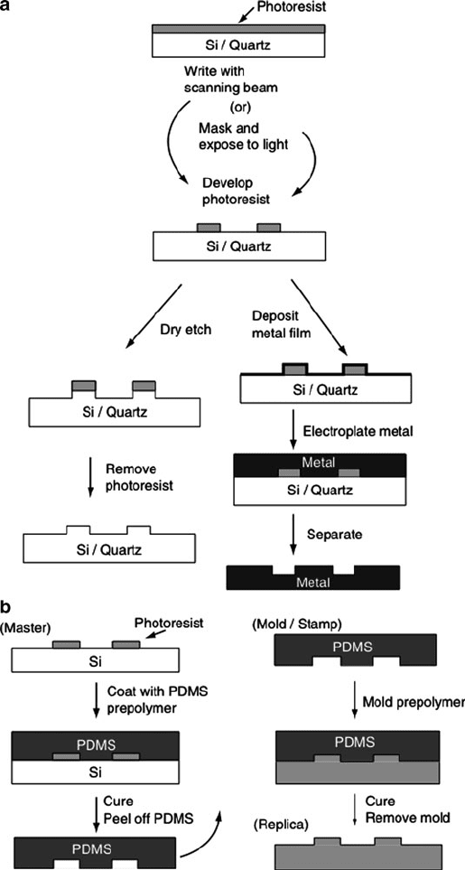
Figure 4.66. Comparison of (a) conventional photolithography/electroplating with (b) soft lithography.
Shown in (b) is replica molding which consists of the formation of a PDMS stamp, and subsequent
replication of a master in a photo- or thermally curable prepolymer. Reproduced with permission from
Gates, B. D.; Xu, Q.; Stewart, M.; Ryan, D.; Willson, C. G.; Whitesides, G. M. Chem. Rev. 2005, 105,
1171. Copyright 2005 American Chemical Society.
314 4 Semiconductors
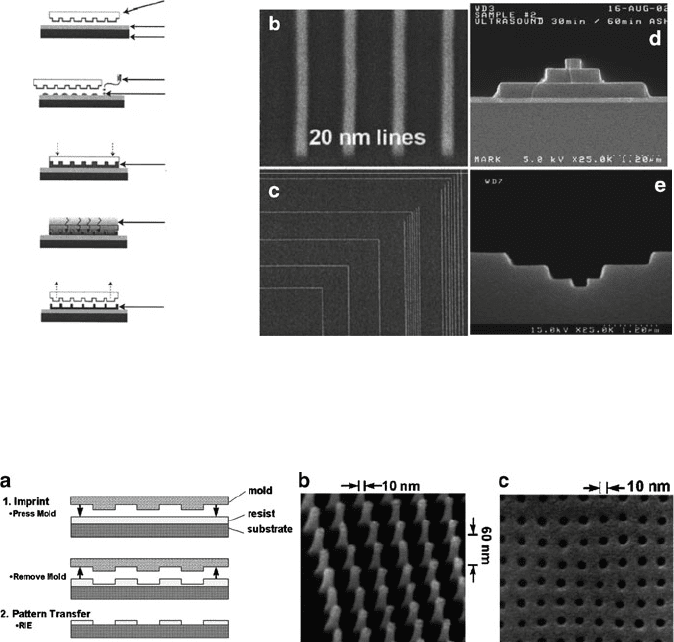
exhibit diffusion during patterning. Hence, the following complementary strategies
have been employed:
(i) Using a composite two-layer stamp comprised of a 30 mm hardened PDMS
coating on a 2–3 mm thick PDMS support
[71]
; especially in tandem with sharp,
V-shaped grooves
(ii) Using high molecular weight inks such as dendrimers
[72]
and biological mole-
cules (e.g., proteins)
Using a combination of the above modifications has now extended nanocontact
printing to well below the 30 nm regime – even as low as 2 nm!
[73]
Though PDM S has dominated the field of soft lithography, DeSimone and cow-
orkers have introduced fluorinated perfluoropolyether (PFPE) elastomers, which
offer better solvent resistanc e and cleaner mold-release characteristics.
[74]
This
Transparent template
(mold)
Planarization layer
Resist dispenser
Imprint resist
Imprint fluid fills
template pattern
UV blanket
exposure
Exact replica of
template pattern
Substrate
Step 1: Orient template and substrate
a
Step 2: Dispense drops of liquid imprint resist
Step 3: Lower template and fill pattern
Step 4: Polymerize imprint fluid with UV exposure
Step 5: Separate template from substrate
Figure 4.67. Schematic of step-and-flash imprint lithography, SFIL. The SEM images shown in (b) and
(c) represent 20- and 40-nm patterned line arrays, whereas (d) and (e) show a multi-tiered template and
resultant imprint in a resist material. Reproduced with permission from J. Microlithogr., Microfabr.,
Microsyst. 2005, 4, 011 002. Copyright 2005 International Society of Optical Engineering.
Figure 4.68. Schematic of nanoimprint lithography (NIL), and SEM images of a nanopatterned mold and
arrays imprinted in poly(methyl methacrylate). Reproduced with permission from J. Vac. Sci. Technol. B
1997, 15, 2897. Copyright 1997 American Institute of Physics.
4.2. Silicon-Based Applications 315
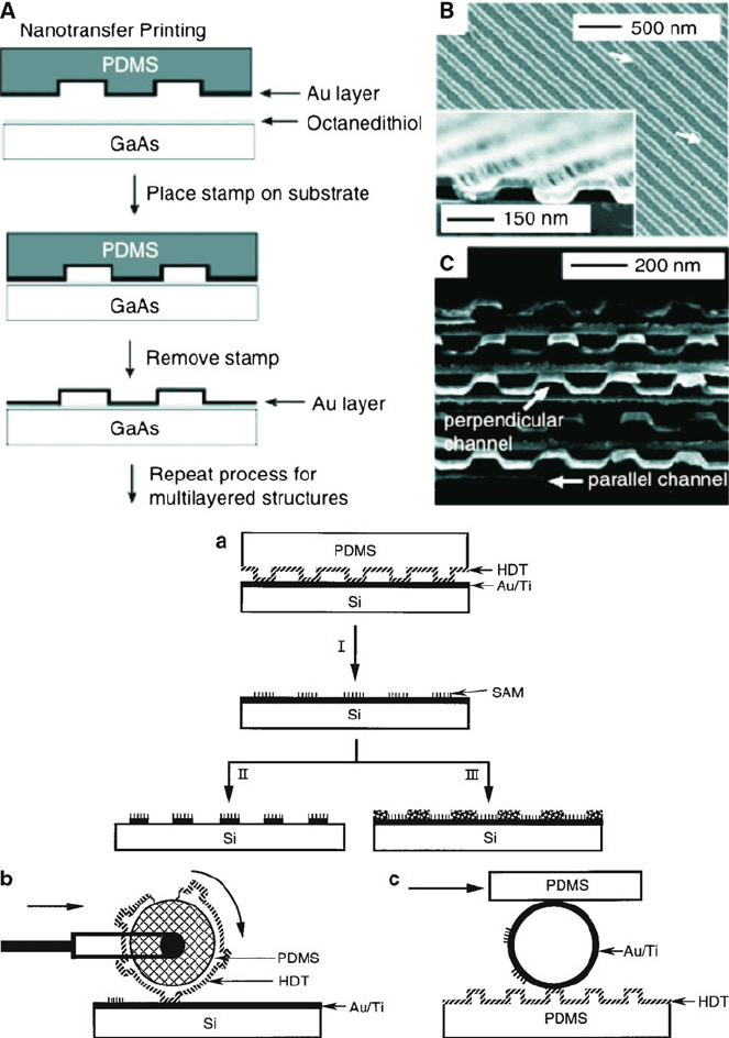
Figure 4.69. Top: Schematic of the general process of nanotransfer printing. SEM image B illustrates a
20-nm grooved gold layer transferred onto a GaAs surface. Image C shows a multilayered stack of 20-nm
thick layers of parallel grooves; the channels in adjacent layers are aligned perpendicular to one another.
Reproduced with permission from Chem. Rev. 2005, 105, 1171. Copyright 2005 American Chemical
Society. Bottom: illustration of the diversity of microcontact printing. Shown is the printing of
hexadecanethiol (HDT) via: (a) a planar surface with a planar stamp (I: SAM printing, II: etching, III:
deposition), (b) large-area printing on a planar surface with a rolling stamp, and (c) printing on a
nonplanar surface with a planar stamp. Reproduced with permission from Angew. Chem. Int. Ed. 1998,
37, 550. Copyright 1998 Wiley-VCH.
316 4 Semiconductors
version of soft lithography is coined PRINT – Particle (or Pattern) Replication in
Nonwetting Templates. Figure 4.71 illustrates the processes involved in the PRINT
technique. A master template with the desired features is first prepared via e-beam
lithography or photolithography/etching of a Si substrate. A homogeneo us coating of
a photocurable liquid PFPE is then applied and photochemically cross-linked to yield
a mold that may be peeled away from the master. To generate a 2-D array of particles
or free particulates, the mold is filled with an appropriate liquid via capillary filling
without wetting the land area around the cavities. The liquid in the mold is then
converted to a solid using evaporation, curing, lyophilization or other mode of phase
transition, and the array may then be transferred to another surface. It should be noted
that this process is also amenable for the replication of naturally-occurring objects
such as virus particles,
[75]
block copolymer micelles, and protein particles.
[76]
The PRINT technique is analogous to micromolding in capillaries (MMIC) or
solvent-assisted micromolding (SAMIM), with the use of perfluorinated polymers
rather than silicones (Figure 4.72). The use of PFPE instead of PDMS molds offers
the following benefits (Figure 4.73)
[77]
:
(i) Lower surface energy and solvent resistance, which allows one to selectively fill
the nanosized cavities of the mold without wetting the surrounding area – giving
rise to a diverse range of particulate morphologies and surface functionalization
(Figure 4.74), of extreme importance for n anomedicine applications
[78]
;
(ii) Non-stick properties allow the organic particles to be easily removed from the
mold.
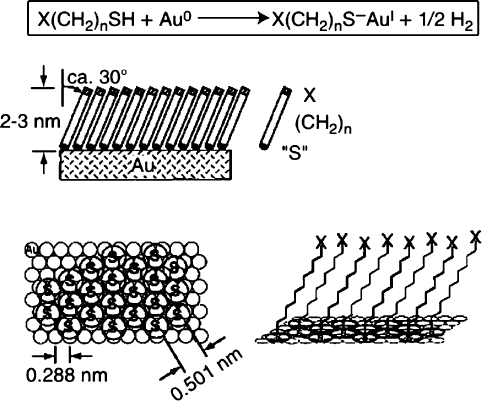
Figure 4.70. Schematic of a self-assembled monolayer (SAM), illustrating the organization of the alkyl
chains via van der Waal interactions, and the close-packed array of sulfur atoms on the gold surface.
Reproduced with permission from Xia, Y.; Whitesides, G. M. Angew. Chem. Int. Ed. 1996, 37, 550.
Copyright 1996 Wiley-VCH.
4.2. Silicon-Based Applications 317