Fahlman B.D. Materials Chemistry
Подождите немного. Документ загружается.

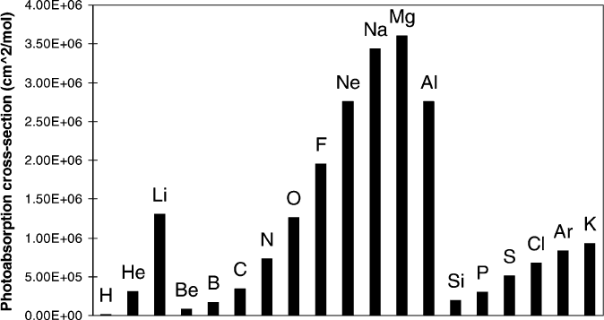
transparent to most materials. Consequently, CAM photoresists may not be used
for EUV photolithography since they are comprised of O and F groups, which possess
the greatest photoabsorption cross-section (Figure 4.47). Instead, the most widely
developed photoresists with increased EUV transparency are based on poly(hydro-
xystyrene), or particularly transparent oxygen-free photoresists such as poly(trimethyl-
silylstyrene-co-chloromethylstyrene) or other silicon-containing polymers.
[36]
However, varying combinations and degrees of polymer swelling, low sensitivities,
and low etch resistances have plagued all EUV photoresists developed to date.
In addition to decreasing the exposure wavelength, an increase in the numerical
aperture of the exposure system will also yield improvements in the resultant line
resolution (Eq. 13).
[37]
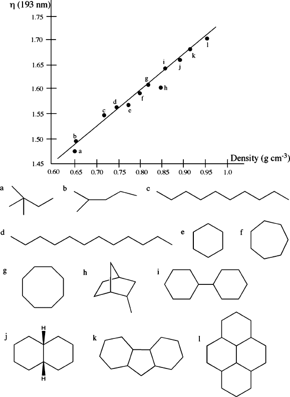
Since the refractive index of the medium is directly propor-
tional to the numerical aperture (NA), one simply needs to surround the lithographic
lens with a fluid of greater refractive index (e.g., water: ¼ 1.47 at 193 nm; air:
¼ 1.0). Though such immersion lithography has been suggested as a candidat e
for sub-50-nm line resolution, there are significant technical challenges (e.g.,
CaF
2
-based optics, which are hygroscopic) that must first be addressed. There are
current research efforts devoted to utilizing highe r-index fluids; thus far, a variety
of candidates have been identified that exhibit a refractive index close to 1.7
(Figure 4.48). However, as one would expect, immersion lithography suffers from
a variety of technical issues such as:
(i) Micro-/nano-sized bubble formation (scattering the incident radiation, causing
significant losses in line resolution
(ii) Con tamination of the immersion fluid by the resist (altering the refractive
index, again hurting line resolution)
(iii) Hea ting the immersion fluid during exposure (resulting in the same effect as ii))
Figure 4.47. Photoabsorption cross-section of different atoms at 13.4 nm. Reproduced with permission
from Polym. Adv. Technol. 2006, 17, 94. Copyright 2006 John Wiley & Sons, Inc.
288 4 Semiconductors
However, it should be noted that in addition to improving resolution via tweaking
the NA, the depth of focus (DOF ¼ l/(NA)
2
) is also paramount for the patterning of
sharp features. As the depth of focus decreases with resolution, it will become
increasingly more difficult to define features simultaneously at the top and bottom
surfaces. Conseque ntly, chemical mechanical polishing (CMP) is used to plan arize
the wafer prior to high-resolution photolithography, and as thin a layer as possible of
photoresist must be applied to the wafer. As its name implies , CMP entails the use of
Figure 4.48. Indices of refraction, densities, and molecular structures of high-Z fluids proposed for
immersion-lithography applications. Adapted with permission from Proc. SPIE 2008, 6923, 69230A-1.
[38]
4.2. Silicon-Based Applications 289
an abrasive, corrosive slurry to physically grind flat and chemically remove the
microscopic topographic features on a wafer so that subsequent processes can begin
from a flat surface.
Etching
Once the pattern in the photoresist layer is formed, a variety of chemical or high-
energy plasma techniques may be used to remove exposed underlying layer(s) – a
process referred to as etching.
[39]
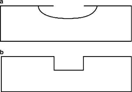
It should be noted that “wet” etching, or dipping
the wafer in an acidic solution, typically results in isotropic etching (Figure 4.49a),
and a line resolution of >2 mm. By contrast, “dry” etching that uses a plasma
[40]
generally results in anisotropic conditions (Figure 4.49b), and line resolutions
<0.25 mm. It has been shown that the pre-application of an adhesion promoter
results in greater anisotropic etching (less undercutting), since the photoresist and
wafer surface are in closer contact with one another.
The specific etching conditions used will depend on the surface to be removed.
For instance, Figure 4.40 illustrated some wet and dry etching conditions to prefer-
entially remove SiO
2
from a Si surface. Tables 4.3 and 4.4 provide a comprehensive
list of wet and dry (plasma) etching recipes that may be used to selectively remove a
variety of materials. Other plasmas used for selective SiO
2
removal include CF
4
/H
2
and C
2
F
6
/CHF
3
. Whereas a plasma of Cl
2
/C
2
F
6
may be used for n-type Si, Cl
2
/argon
is used for undoped Si. The addition of oxygen to a fluorocarbon plasma increases
the amount of free F through the formation of oxyfluorides from fluorocarbons
(Eq. 14).
[41]
However, if more than 10% O
2
is added to the plasma, a decrease in
the Si etching rate will result. Most likely, this is due to the competition between O
and F atoms for active sites on the silicon surface. Recipes used to remove Si
3
N
4
layers include CF
4
/H
2
or SF
6
/O
2
combinations, which generate reactive fluorine
species within the plasma (Eq. 15). It should be noted that O
2
/H
2
O and O
2
/CF
4
Figure 4.49. Illustration of (a) isotropic etching evidenced by severe undercutting and (b) anisotropic
etching with 90
sidewall channels (or vias).
290 4 Semiconductors

Table 4.3. Wet Etching Recipes
Material to
be etched
Recipe Comments
Al 16:2:1:1 H
3
PO
4
:water:acetic
acid:HNO
3
PAN etch; 200 nm/min at 25
C;
600 nm/min at 25
C
Al Conc. H
3
PO
4
At 120
C
Ag 1:1 NH
4
OH:H
2
O
2
Au 3:1 HCl:HNO
3
Aqua regia
Cr 3:1 HCl:water
Cu 5:1 HNO
3
:water
Fe 1:1 HCl:water
Fe 1:1 HNO
3
:water
Mo 1:1 HCl:H
2
O
2
Mo 1:1:1 H
2
SO
4
:HNO
3
:water
Ni 5:1 HCl:HNO
3
Ni 1:1 HF:HNO
3
Pb 2:2:5 acetic acid:H
2
O
2
:water
Pb 1:1 acetic acid:H
2
O
2
Pd 3:1 HCl:HNO
3
Pt 3:1:4 HCl:HNO
3
:water At 95
C
Pt 8:1 HCl:HNO
3
At 70
C
PolySi 3:1 HNO
3
:HF 4.2 mm/min at 25
C
PolySi 50:20:1 HNO
3
:water:HF 540 nm/min at 25
C
Si 2:2:1 HF:HNO
3
:water
Si 5:3:3 HNO
3
:HF:acetic acid
SiO
2
6:1 NH
4
F:HF 120 nm/min at 25
C
SiO
2
1:10 HF:water 30 nm/min at 25
C
SiO
2
1:100 HF:water 1.8 nm/min at 25
C
SiO
2
conc. HF 1.8 mm/min at 25
C
Si
3
N
4
refluxing H
3
PO
4
At 180
C
Sn 1:1 HF:HNO
3
Ta 2:2:5 HF:HNO
3
:water
Ti 1:30:69 HF:H
2
SO
4
:water At 70
C
Ti/W alloy H
2
O
2
5 nm/min at 25
C
W 1:1 HF:HNO
3
Table 4.4. Dry (Plasma) Etching Recipes
Material to
be etched
Recipe Comments
Al 10 sccm Cl
2
BCl
3
(30 sccm) is added to scavenge O in the native oxide
layer; 180 mTorr (30 mTorr results in anisotropic etch);
200 W; 0.5 mm/min
polySi 30 sccm Cl
2
(isotropic);
5:25 sccm Cl
2
:HBr
180 mTorr (isotropic); 30 mTorr (anisotropic); 100 W; 0.5 mm/
min (isotropic); 0.3 mm/min (anisotropic)
SiO
2
45:5 sccm CF
4
:O
2
150 mTorr; 100 W; 0.15 mm/min
Si
3
N
4
45:5 sccm SF
6
:O
2
150 mTorr; 100 W; 0.2 mm/min
Polyimide 47:3 sccm O
2
:CF
4
200 mTorr; 20 W; 1 mm/min
4.2. Silicon-Based Applications 291
plasmas, or high-temperature annea ling, are typically used to remove the photoresist
that remains following the wet/dry etching. However, in order to remove non-
postbaked photoresists, simple washing with organic solvents is often sufficient (e.
g., positive tone photoresists: acetone, trichloroethylene (TCE); negative tone
photoresists: methyl ethyl ketone (MEK, CH
3
C(O)C
2
H
5
), methyl isobutyl ketone
(MIBK, CH
3
C(O)C
4
H
9
).
CF
4
þO !
plasma
COF
2
þ 2Fð14Þ
Si
3
N
4
þ 12 F !
plasma
3 SiF
4
þ2N
2
ð15Þ
So far, we have progressed through steps (a)–(c) of the stepwise CMOS IC
process (Figure 4.39), with patterning and sequential selective etching to yield a
channel (referred to as a via) through both the protective oxide/nitride layers and the
underlying Si substrate. The resulting trench will be eventually back-filled with SiO
2
(Figure 4.39, step e), which serves to electrically isolate individual devices on the
chip from one another. This process, referred to as shallow trench isolation (STI), is
the method- of-choice for modern CMOS fabrication since it allows the deposition of
smaller insulating regions resulting in greater device density, in accord with
Moore’s Law.
Step (d) of Figure 4.39 illustr ates the deposition of a thin film (ca. 10–20 nm)
of SiO
2
onto the trench sidewalls and bottom. This is used to establish an effective
SiO
2
/Si interface prior to the deposition of the thick (ca. 500 nm–1 mm) back-
filled SiO
2
layer. That is, to ensure that the SiO
2
conforms to the entire channel
surface, leaving no void spaces that would decrease the effectiveness of the isolation
trench. Once the thick oxide is deposited into the trench, chemical mechanical
polishing (CMP) is used for planarization of the surface prior to subsequent layering
steps (Figure 4.39, step f).
[42]
The silicon nitride layer acts a polishing stop, and
is subsequently removed through plasma etching.
Ion implantation
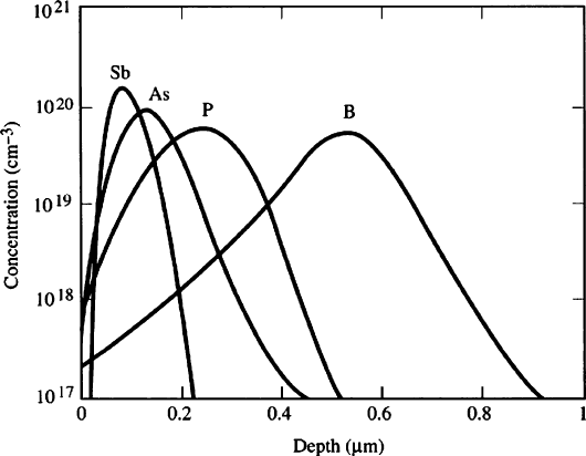
The next steps (Figure 4.39g–i) involve the placement of n- and p-type dopants onto
the top of the silicon surface. A technique known as ion implantation involves the
acceleration of B (p-type) or Sb/As/P (n-type) ions to very high kinetic energies
(ca. 50–200 keV), which then collide with the Si lattice. The chosen energy must be
sufficient to penetrate through the SiO
2
layer and a desired depth of Si substrate, but
not the exposed photoresist layer that defines the dopant region. For the same
accelerating voltage, ions of smaller mass will penetrate to deeper/broader regions
of the solid relative to heavier ions (Figure 4.50), due to differences in their kinetic
energies and concomitant collisions with Si atoms.
An energy on the order of 15 eV is enough to dislodge a Si atom from its
crystalline lattice, forming a Frenkel defect. However, the energies of the impinging
dopant ions are an order of magnitude larger, which will cause significant damage to
292 4 Semiconductors
the Si crystal structure. For instance, bomb ardment of a Si surface with a single
arsenic ion with an energy of 30 keV will displace 1,000 Si atoms – all on a
timescale of ca.10
13
s! Multiply this by thousands of bombarding ions during
the implantation process, and one has a picture of a highly perturbed Si crystal.
Amazingly, thermal annealing is able to cause the dislodged Si atoms to find vacant
sites, remov ing the Frenkel defects and thus repair the damage. Prolonged high-
temperature annealing at temper atures of 1,000–1,100
C is subsequently used to
further restore the periodicity of the Si crystal lattice, and diffuse the n- and p-dopant
wells (i.e., the substrates for pMOS and nMOS devices, respectively) to their desired
Si depths of ca.2mm. It should be noted that the above ion bombardment processes
are repeated using an appropriate masking photoresist to introduce a higher concen-
tration of dopants near the surface of the n and p wells. This is done to adjust the
threshold voltages (V
T
) of the nMOS and pMOS devices (Figure 4.39, step i).
Steps (j)–(k) of Figure 4.39 illustrate the formation of the gate electrodes onto the
nMOS and pMOS devices. This consists of the deposition of a ca. 500 nm thick
polysilicon
[43]
film onto the wafer surface, and subsequent photolithography/etching
steps. The specific methodologies used for thin-film deposition will be described in
the next section of this chapter. The source and drain of the complimentary MOS
devices are shown in step (l); this is performed through careful ion bombardment
using an appropriate photolithographic mask. Also shown in step (l) is the deposition
of insulating SiO
2
on the sidewalls of the polysilicon gate.
[44]
Figure 4.50. Comparison of the Si depth penetration of various n- and p-dopant ions. Reproduced with
permission from Plummer, J. D.; Deal, M. D.; Griffin, P. B. Silicon VLSI Technology, Prentice-Hall:
New York, 2000.
4.2. Silicon-Based Applications 293

Now that the source/drain and gate electrodes have been formed for nMOS and
pMOS complimentary devices, the remaining steps involve metalation – the selec-
tive deposition of metals that form the interconnection between the active devices on
the IC. Step m of Figure 4.39 shows the deposition of titanium onto the IC surface,
followed by annea ling at a temperature of 600
C under a nitrogen environment.
Although Ti will readily react with the ambient N
2
to form TiN, titanium will also
readily react with Si atoms to form TiSi
2
in the regions where a Ti/Si interface exists
(at the top of the polysilicon gate, and source/drain cavities). The dark regions
illustrated in step (n) of Figure 4.39 indicate the regions of TiSi
2
, with TiN formed
in all other areas. Metal silicides are used to reduce the resistivity of the polysilicon
gate; in addition to TiSi
2
, other analogues such as WSi
2
, and CoSi
2
are frequently
utilized. The exposed TiN is subsequently patterned usin g a photolithographic mask,
and is etched using a 1:1:5 NH
4
OH:H
2
O
2
:H
2
O wet etching solution (step o).
A thick layer (ca.1mm) of insu lating oxide is then deposited onto the evolving IC,
which serves as the interconnect dielectric medium. Although SiO
2
was typically
used for this purpose, the latest ICs utilize a high-k dielectric such as carbon-doped
SiO
2
(Figure 4.51) that is reported to increase the capacitance by up to 20% relative
to undoped media. This improvement translates to higher perform ance at lower
power consumption – paramount for high-density modern ICs. Following planariza-
tion of the oxide layer (Figure 4.39, step p), selected regions are patterned/etched
using our workhorse of photolithography (Figure 4.39, step q). The etched regions
are then back-filled with another metal (usually W or Co); however, to improve the
adhesion and electrical properties of the interface, a thin buffer layer of TiN is first
deposited (Figure 4.39, step r). Subsequent planarization results in a flat surface
containing isolated regions of tungsten.
Figure 4.51. Cross-section TEM image of the placement of a carbon-doped oxide (CDO) dielectric
between metal interconnects. Reproduced with permission from Intel Corporation (http://www.intel.com).
294 4 Semiconductors

The final steps involve deposition of the interconnect metal (Figure 4.39, step s).
Copper is now the metal-of-choice due to its more desirable electrical resistivity,
relative to Al (1.7 mO cm vs. 2.7 mO cm, respectively) that was exclusively used in
earlier ICs. Due to its low resistivity and high density, titanium nitride is an efficient
barrier level that prevents surface oxidation of Cu, as well as the interdiffusion of Cu
into adjacent layers. To yield the final multilayer IC shown in step t of Figure 4.39,
steps (p)–(s) are repeated. Indeed, a long complex process that took weeks in the
making.
Perhaps a topic that has been overshadowed by the previous detailed discussion of
high-k dielectrics is the use of materials at the other end of the capacitance spectrum:
low-k dielectrics. In ICs, insulating dielectrics separate the conductive portions
(e.g., wire interconnects and individual transistors) from one another. In order to
fabricate chips with higher speeds, the transistors must be placed closer and closer
together, thus resulting in a thinner insulating layer. This leads to charge buildup and
crosstalk, which adversely affects the maximum operating speed and performance of
the chip. The use of low-k dielectrics is important to reduce the parasitic capaci-
tance, hence enabling faster switching speeds and lower heat dissipation. Doping
SiO
2
with fluorine reduces the k from 3.9 to 3.5; other approaches that yield values
of k < 1.5 involve the use of nanoporous dielectrics based on poly(amidoamine-
organosilicon) (PAMAMOS) films (see Chapter 5).
One has to remember that these multistep processes were not performed from start
to finish, one IC at a time. If that were the case, each chip would cost millions
of dollars! Instead, a large polished wafer that is currently 300 mm in diameter is
used as the base to assemble hundreds of ICs (called dies when they are perforated
from the large wafer). It is easy to see why the semiconductor industry has shifted to
larger-diameter wafers; though the fabrication facility (known as a fab) costs billions
of dollars to establish, the price/chip is miniscule since one is essentially able to
assemble hundreds of chips at once (ca. 700 chips/wafer using 300 mm wafers
(Eq. 16 – an increase of over 200% relative to 200 mm). It has been proposed that
the industry will shift to 450 mm wafers in the near future; however, this will
dramatically increase the costs associated with single-crystal ingot processing.
Dies/wafer =
pðwafer diameter=2Þ
2
die area
pðwafer diameterÞ
ffiffiffiffiffiffiffiffiffiffiffiffiffiffiffiffiffiffiffiffiffiffi
2(die area)
p
ð16Þ
It is interesting to note that although each wafer goes through the entire CMOS
fabrication pathway, all of the completed chips/dies may not be equal. Th at is,
microprocessor chips running at 900 MHz and 1.5 GHz may have been produced on
the same wafer! From our detailed discussion of CMOS fabrication, it is not hard
to see how neighboring chips may have slight variations in layer thicknesses/
composition, contaminants, etc. that will significantly alter their ultimate performance.
As you might expect, it is typical for companies to sell the fastest of the fabricated chips
at a premium price, and decrease the price accordingly for slower ones.
4.2. Silicon-Based Applications 295
Thin-film deposition methodologies
The previous section described the deposition of a number of films onto the growing
IC, from insulating SiO
2
layers to the copper interconnects. As you might imagine,
a number of growth strategies are employed to yield the most desirable films for the
particular application. In IC fabrication, individual layers are deposited with varying
levels of thicknesses. For instance, relatively thick layers such as photoresist and
interconnect dielectrics may be deposited with a higher variability in film thickness.
However, for layers such as gate oxide and TiSi
2
, techniques that are able to deposit
films a monolayer at a time are required.
In addition to the application of adhesion promotors and photoresists during IC
fabrication, “bulk” deposition techniques such as dip- or spin-coating are commonly
used for decorative and/or protective coating applications. Films of organic or
inorganic (e.g., sol–gels) materials are also spin-coated onto a desired substrate,
air-dried to remove the solvent, and postannealed (if desired) to yield the appropriate
morphology/porosity of the final film.
[45]
It is possible to control the film thick-
ness during spin-coating through varying the solvent, spin rate, drop height, etc.
However, this technique is not suitable for the growth of thin films where control
over film-thickness homogeneity, morphology, composition, conformality, and
selectivity are paramount to resultant performance.
As we mentioned in the Introduction, the “bottom-up” approach to materials
design, or building the structure one molecule/atom at a time, provides the ultimate
in control over the final properties of the material. For thin-film growth, this
corresponds to vapor deposition techniq ues, rather than the “top-down” approaches
of dip- and spin-coating.
Vapor deposition techniques feature the introduction of gaseous molecular/atomic
subunits that self-assemble on the surface of the substrate to yield the desired film.
The rate of deposition is on the order of A
˚
min
1
, which allows for intimate control
over the properties of the growing film. There are two types of vapor deposition
methods: physical vapor deposition (PVD) and chemical vapor deposition (CVD).
Both methods may be used to grow thin films of metals, alloys, oxides, nitrides,
carbides, silicon, or amorphous/graphitic carbon. PVD may occur through the
evaporation of atoms/molecules from a precursor solid in vacuo (evaporation,
Figure 4.52a), or through use of a high-energy Ar plasma source that causes the
vaporization of atoms from a solid target (sputtering, Figure 4.52b).
[46]
Since all
atoms of the solid in both techniques will enter the gas phase, the resultant film is
only as pure as the solid precursor that is used. As a result, high-purity precursors
must be used for PVD; for example, a piece of gold foil of purity >99.99999%
is typically used as a target for Au sputtering.
In general, coatings produced by the PVD process are hard, with a high atomic
density due to slow and efficient nucleation /growth. Depending on the exposure time
of the substrate with the plasma, the thickness of PVD coatings ranges from a few
angstroms to >30 mm. Since the substrate is maintained at room temperature,
there are no limitations related to the thermal stability of the substrate. This is
296 4 Semiconductors
an important consideration for coating materials that will decompose at high
temperatures such as plastics, paper, etc.
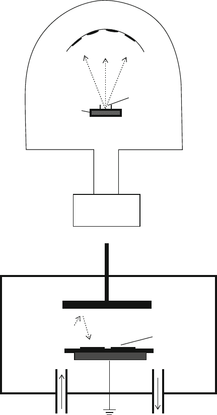
Two methods for the evaporation of precursors may be employed – resistance
heating and electron beam collision. The first method employs a simple alumina
Wafers
Sample
Crucible
Resistive
Heater
Vacuum
Pump
Vacuum
Pump
Ar Plasma
Heater
Wafers
Anode
Ar gas
Inlet
Ground
Target
(Cathode)
a
b
M
Ar
-
e
-
c
-
Ar
-
Ar
MM
M
M
< 10
-6
Torr
Figure 4.52. Schematic of physical vapor deposition apparati. Shown are: (a) an evaporation system and
(b) a sputtering system.
4.2. Silicon-Based Applications 297