Guozhong Cao. Nanostructures & Nanomaterials: Synthesis, Properties & Applications
Подождите немного. Документ загружается.

186
Nanostructures and Nanomaterials
NITROGEN-COOLED
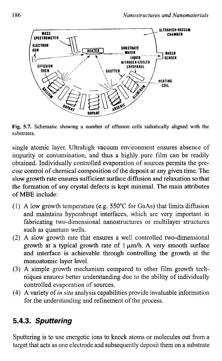
Fig. 5.7.
Schematic showing a number of effusion cells radiatically aligned with the
substrates.
single atomic layer. Ultrahigh vacuum environment ensures absence of
impurity or contamination, and thus a highly pure film can be readily
obtained. Individually controlled evaporation of sources permits the pre-
cise control of chemical composition
of
the deposit at any given time. The
slow growth rate ensures sufficient surface difksion and relaxation so that
the formation
of
any crystal defects is kept minimal. The main attributes
of
MBE
include:
(1)
A
low growth temperature (e.g.
550°C
for GaAs) that limits diffusion
and maintains hyperabrupt interfaces, which are very important in
fabricating two-dimensional nanostructures or multilayer structures
such as quantum wells.
(2)
A
slow growth rate that ensures a well controlled two-dimensional
growth at a typical growth rate of
1
pdh.
A
very smooth surface
and interface is achievable through controlling the growth at the
monoatomic layer level.
(3)
A
simple growth mechanism compared to other film growth tech-
niques ensures better understanding due to the ability of individually
controlled evaporation of sources.
(4)
A
variety of
in
situ analysis capabilities provide invaluable information
for the understanding and refinement of the process.
5.4.3.
Sputtering
Sputtering is to use energetic ions to knock atoms or molecules out from a
target that acts as one electrode and subsequently deposit them on a substrate
Two-Dimensional Nanostructures: Thin Films
187
-V(DC)
MATCHING
-
INSULATION
-
GLOW DISCHARGE GLOW DISCHARGE
SPUTTERING VACUUM
GAS
..
SPUTTERING
VACUUM
GAS
-
INSULATION
-
r
TARGET
-+
GLOW DISCHARGE GLOW DISCHARGE
ANODE
---+
SPUTTERING VACUUM SPUTTERING VACUUM
GAS GAS
i
DC
AF
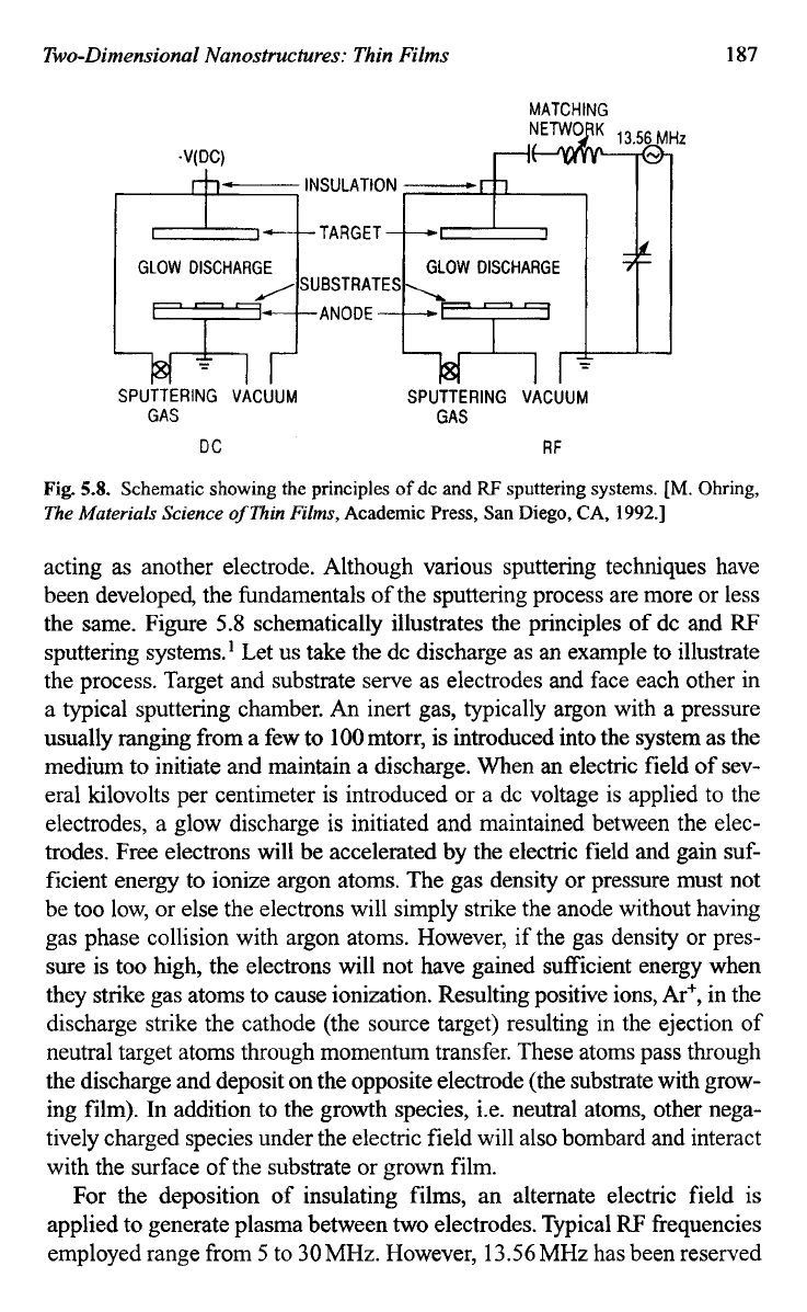
Fig.
5.8.
Schematic showing
the
principles
of
dc and
RF
sputtering systems.
[M.
Ohring,
The Materials Science
of
Thin Films,
Academic Press, San Diego, CA,
1992.1
acting as another electrode. Although various sputtering techniques have
been developed, the fundamentals of the sputtering process are more or less
the same. Figure
5.8
schematically illustrates the principles of dc and
RF
sputtering systems.' Let
us
take the dc discharge as an example to illustrate
the process. Target and substrate serve as electrodes and face each other in
a typical sputtering chamber. An inert gas, typically argon with a pressure
usually ranging from a few to
100
mtorr, is introduced into the system as the
medium to initiate and maintain a discharge. When
an
electric field of sev-
eral kilovolts per centimeter is introduced or a dc voltage is applied to the
electrodes, a glow discharge is initiated and maintained between the elec-
trodes. Free electrons will be accelerated by the electric field and gain suf-
ficient energy to ionize argon atoms. The gas density or pressure must not
be too low, or else the electrons will simply strike the anode without having
gas phase collision with argon atoms. However, if the gas density or pres-
sure is too high, the electrons will not have gained sufficient energy when
they strike gas atoms to cause ionization. Resulting positive ions, Ar+, in the
discharge strike the cathode (the source target) resulting in the ejection
of
neutral target atoms through momentum transfer. These atoms pass through
the discharge and deposit on the opposite electrode (the substrate with grow-
ing film). In addition to the growth species, i.e. neutral atoms, other nega-
tively charged species under the electric field will also bombard and interact
with the surface of the substrate or grown film.
For the deposition of insulating films, an alternate electric field is
applied to generate plasma between
two
electrodes. Typical
RF
frequencies
employed range from
5
to
30MHz.
However,
13.56
MHz
has been reserved
188
Nunostructures
and Nunomuterials
for plasma processing by the Federal Communications Commission and is
widely used. The key element in
RF
sputtering is that the target self-biases
to
a
negative potential and behaves like a dc target. Such a self-negative tar-
get bias is a consequence of the fact that electrons are considerably more
mobile than ions and have little difficulty in following the periodic change
in the electric field. To prevent simultaneous sputtering on the grown film
or substrate, the sputter target must be an insulator and be capacitively cou-
pled to the
RF
generator. This capacitor will have a low
RF
impedance and
will allow the formation of a dc bias on the electrodes.
It should also be noted that the types of plasmas encountered in thin
film processing techniques and systems are typically formed by partially
ionizing a gas at a pressure well below atmospheric. For the most part,
these plasmas are very weakly ionized, with an ionization fraction of
1
0-5
to
lo-'.
Although the above discussion is focused on the deposition of
films by sputtering, plasma or glow discharges are widely used in other
film processes, such as plasma etching.14 Other examples include plasma
enhanced chemical vapor deposition
(PECVD),
ion plating and reactive
ion etching (RIE). The plasma based film processes differ from other film
deposition techniques such as evaporation, since the plasma processes is
not thermal and not describable by equilibrium thermodynamics.
Sputtering a mixture
of
elements or compounds will not result in a
change
of
composition in the target and thus the composition of the vapor
phase will be the same as that of the target and remain the same during
the deposition. Many modifications have been made to enhance or
improve the deposition process and resulted in the establishment of
hybrid and modified
PVD
processes. For example, magnetic field has
been introduced into sputtering processes to increase the residence time of
growth species in the vapor phase; such sputtering is referred to as mag-
netron sputtering. Reactive gases have also been introduced into the dep-
osition chamber to form compound films, which are known as reactive
sputtering.
5.4.4.
Comparison
of
evaporatjon and sputtering
Some major differences between evaporation and sputtering are briefly
summarized below:
(1)
The deposition pressure differs noticeably. Evaporation uses low pres-
sures typically ranging from to torr, whereas sputtering
requires a relatively high pressure typically of -100torr. Atoms or
molecules in evaporation chamber do not collide with each other,
Two-Dimensional Nanostructures: Thin Films
189
whereas the atoms and molecules in sputtering do collide with each
other prior to arrival at the growth surface.
(2)
The evaporation is a process describable by thermodynamical equi-
librium, whereas sputtering is not.
(3)
The growth surface is not activated in evaporation, whereas the
growth surface in sputtering
is
constantly under electron bombard-
ment and thus is highly energetic.
(4) The evaporated films consist of large grains, whereas the sputtered
films consist of smaller grains with better adhesion to the substrates.
(5)
Fractionation of multi-component systems is a serious challenge in
evaporation, whereas the composition
of
the target and the film can be
the same.
5.5.
Chemical Vapor Deposition (CVD)
CVD
is
the process
of
chemically reacting a volatile compound of a mate-
rial to be deposited, with other gases, to produce a nonvolatile solid that
deposits atomistically on a suitably placed substrate.'
CVD
process has
been very extensively studied and very well d~cumented,'~-'~ largely due
to the close association with solid-state microelectronics.
5.5.1.
Typical
chemical
reactions
Because of the versatile nature of
CVD,
the chemistry is very rich, and
various types of chemical reactions are involved. Gas phase (homogeneous)
reactions and surface (heterogeneous) reactions are intricately mixed. Gas
phase reactions become progressively important with increasing tempera-
ture and partial pressure of the reactants. An extremely high concentration
of reactants will make gas phase reactions predominant, leading to
homogeneous nucleation. For deposition of good quality films, homoge-
neous nucleation should be avoided. The wide variety of chemical reac-
tions can be grouped into: pyrolysis, reduction, oxidation, compound
formation, disproportionation and reversible transfer, depending on the
precursors used and the deposition conditions applied. Examples of the
above chemical reactions are given below:
(A)
Pyrolysis or thermal decomposition
SiH4(g)
+
Si(s)
+
2H2(g)
at
650°C
Ni(C0)4(g) +Ni(s)
+
4CO(g) at
180°C
(5.15)
(5.16)
190
Nanostructures and Nanomaterials
(B)
Reduction
SiC14 (g)
+
2H2(g)
+
Si(s)
+
4HCl(g) at 1200°C
WF&)
+
3H2(g)
-+
W(s)
+
6HF(g) at 300°C
SiH4(g)
+
02(g)
-+
Si02(s)
+
2H2(g) at 450°C
4PH3(g)
+
502(g)
+
2P205(s)
+
6H&) at 450°C
SiC14(g)
+
CH4(g)
-+
SiC(s)
+
4HCl(g) at 1400°C
TiC14(g)
+
CH4(g)
-+
TiC(s)
+
4HCl(g) at 1000°C
2 Ge12(g)
+
Ge(s)
+
Ge14(g) at 300°C
(C) Oxidation
(D) Compound formation
(E)
Disproportionation
(F) Reversible transfer
As&)
+
As&)
+
6GaCKg)
+
W(g)
6GaAs(s) +6HCl(g) at 750°C
(5.17)
(5.18)
(5.19)
(5.20)
(5.21)
(5.22)
(5.23)
(5.24)
The versatile chemical nature
of
CVD process is further demonstrated by
the fact that for deposition of a given film, many different reactants or
precursors can be used and different chemical reactions may apply. For
example, silica film is attainable through any of the following chemical
reactions using various
:
SiH4(g>
+
02(g)
-9
Si02(s)
+
2H2(g) (5.25)
SiH4(g)
+
2N2O(g)
-+
Si02(s)
+
2H2(g)
+
2N2(g) (5.26)
SiH2C12(g)
+
2N20(g)
-+
SiO,(s)
+
2HCl(g)
+
2N2(g) (5.27)
Si2C16(g)
+
2N20(g)
-+
Si02(s)
+
3Cl2(g)
+
2N2(g) (5.28)
Si(OC2H5)4(g) sio2(s)
+
4C2Hdg) 2H2O(g) (5.29)
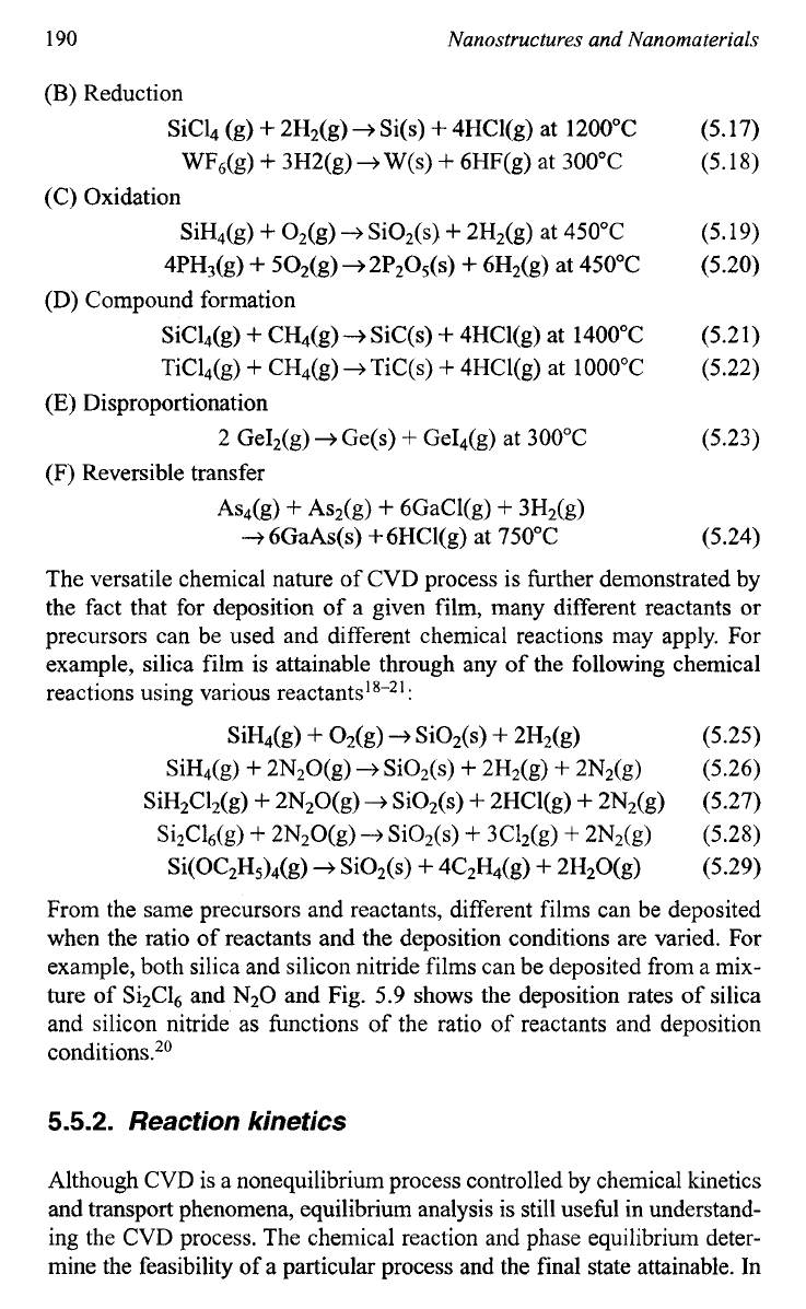
From the same precursors and reactants, different films can be deposited
when the ratio of reactants and the deposition conditions are varied. For
example, both silica and silicon nitride films can be deposited from a mix-
ture of Si2C16 and
N20
and Fig.
5.9
shows the deposition rates of silica
and silicon nitride as functions
of
the ratio
of
reactants and deposition
conditions.20
5.5.2.
Reaction kinetics
Although CVD is a nonequilibrium process controlled by chemical kinetics
and transport phenomena, equilibrium analysis is still useful in understand-
ing the CVD process. The chemical reaction and phase equilibrium deter-
mine the feasibility of a particular process and the final state attainable. In
Two-Dimensional Nanostructures: Thin Films
lo.oo
t
Sih
Si3N4
10
SCCM
Si2C16
FLOW
t
191
0
5
10
IS
20
25
30
R
0.01
Fig.
5.9.
Deposition rates
of
silica and silicon nitride as functions
of
the ratio of reactants
and deposition conditions.
[R.C.
Taylor and
B.A.
Scott,
1
Electrochem.
SOC.
136,
2382
(1
989).]
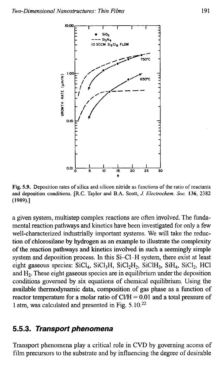
a given system, multistep complex reactions are often involved. The funda-
mental reaction pathways and kinetics have been investigated for only a few
well-characterized industrially important systems. We will take the reduc-
tion of chlorosilane by hydrogen as an example to illustrate the complexity
of
the reaction pathways and kinetics involved in such a seemingly simple
system and deposition process. In this Si-Cl-H system, there exist at least
eight gaseous species: SiCl,, SQH, SiC12H2, SiClH,, SiH,, SiC12, HC1
and HZ. These eight gaseous species are in equilibrium under the deposition
conditions governed by six equations
of
chemical equilibrium. Using the
available thermodynamic
data,
composition of gas phase as a hction of
reactor temperature for a molar ratio
of
Cl/H
=
0.01
and a total pressure of
1 atm, was calculated and presented in Fig.
5.
5.5.3.
Transport phenomena
Transport phenomena play a critical role in CVD by governing access
of
film precursors to the substrate and by influencing the degree of desirable
192
Nanostructures and Nanomaterials
t
h
E
Y
v
Temperature
(K)
Fig.
5.10.
Composition of gas phase as
a
function
of
reactor temperature
for
a
molar ratio
of
Cl/H
=
0.01 and a total pressure
of
1
atm, calculated using
the
available thermodynamic
data.
[E.
Sirtl,
L.P.
Hunt, and D.H. Sawyer,
.I
Electrochem.
SOC.
121,
919
(1974).]
and unwanted gas phase reactions taking place before deposition. The
complex reactor geometries and large thermal gradient characteristics of
CVD chambers lead
to
a wide variety of
flow
structures that affect film
thickness, compositional uniformity and impurity
level^.'^
For CVD reactors operating at a low pressure, where the mean free path
of gas molecules is
10
times larger than the characteristic length of the
reactor, there is no collision between gas molecules and thus the transport
of gas is in the free molecular flow regime. For most CVD systems, the
characteristic pressure is
0.01
atm and above, and the mean free paths are
far larger than the characteristic system dimension. In addition, the gas
velocities are low in most CVD reactors, typically of tens of cdsec, the
Reynolds number is typically less than
100
and the flows are laminar.
As
a result,
a
stagnant boundary layer of thickness,
6,
adjacent to the growth
surface is developed during the deposition. In this boundary layer, the
composition
of
growth species decreases from the bulk concentration,
Pi,
to the surface concentration above the growing film,
Pio,
and the growth
species diffuses through the boundary layer prior to depositing onto the
growth surface as discussed in Chapter
3
and also illustrated in Fig.
3.6.
Two-Dimensional Nanostructures: Thin
Films
193
When the perfect gas laws are applied since the gas composition in the
typical
CVD
systems is reasonably dilute, the diffision flux of gas or
growth species through the boundary layer is given by:
(5.30)
Where
D
is the diffisivity and is dependent on pressure and temperature:
D
=Do
(")
(r)'
p
To
(5.3
1)
where
n
is
experimentally found to be approximately
1.8.
The quantity
Do
is the value
of
D
measured at standard temperature
To
(273
K)
and pressure
Po
(1
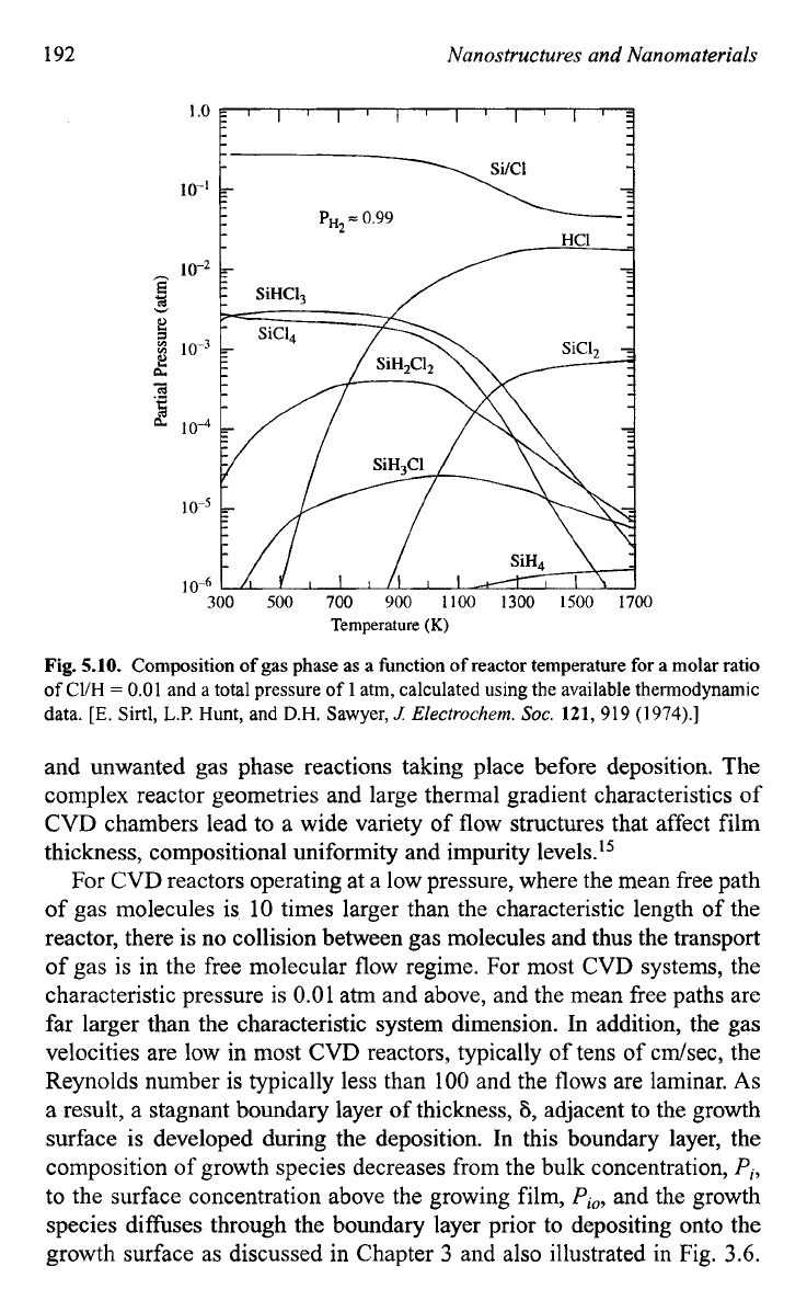
atm), and depends on the gas combination in question. Figure
5.1
1
shows the deposition rate of silicon from four different precursor gases as
a function of temperat~re.~~ This figure also shows that the deposition of
silicon films becomes difision controlled at high substrate temperatures,
whereas surface reaction is a limiting process at relatively low substrate
temperatures.
When growth rate is high and the pressure in the reactor chamber is
high, difision of growth species through the boundary layer can become
a rate-limiting process.
As
Eq.
(5.3
1)
indicated, the gas difisivity varies
inversely with pressure, and thus the diffusion flux of gas through the
-
SUBSTRATE TEMPERATURE
,
OC
0.7
OB
0.9
1
.o
1.1
103
SUBSTRATE TEMPERATURE,
-
-
T(K)
Fig.
5.11.
Deposition rate
of
silicon
from
four
different precursor gases as a function
of
temperature.
[
W.
Kern,
in
Microelectronic Materials and Processes,
ed.
R.A.
Levy,
Kluwer,
Boston,
MA,
p.
203,
1989.1
194
Nanostructures and Nanomaterials
boundary layer can be enhanced simply by reducing the pressure in the
reactor. For deposition of large area films, depletion
of
growth species or
reactants above the growth surface can result in non-uniform deposition
of films.
To
overcome such non-uniformity in deposited films, various
reactor designs have been developed to improve the gas-mass transport
through the boundary layer. Examples include using low pressure and new
designs of reactor chambers and substrate susceptors.
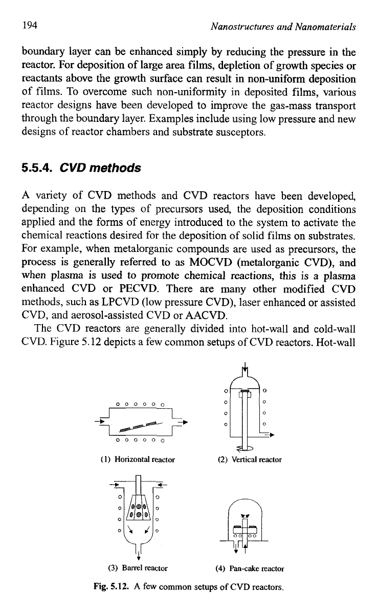
5.5.4.
CVD
methods
A
variety of
CVD
methods and
CVD
reactors have been developed,
depending on the types of precursors used, the deposition conditions
applied and the forms of energy introduced to the system to activate the
chemical reactions desired for the deposition of solid films on substrates.
For example, when metalorganic compounds are used as precursors, the
process is generally referred to as
MOCVD
(metalorganic
CVD),
and
when plasma is used to promote chemical reactions, this is a plasma
enhanced
CVD
or
PECVD.
There are many other modified
CVD
methods, such as
LPCVD
(low pressure
CVD),
laser enhanced or assisted
CVD,
and aerosol-assisted
CVD
or
AACVD.
The
CVD
reactors are generally divided into hot-wall and cold-wall
CVD.
Figure
5.12
depicts a few common setups of
CVD
reactors. Hot-wall
A
000000
-
000000
(1)
Horizontal reactor
O$?O
(3)
Barrel
reactor
*
(2)
Vertical
reactor
(4)
Pan-cake
reactor
Fig.
5.12.
A
few
common
setups
of
CVD
reactors.
Two-Dimensional Nanostructures: Thin Films
195
CVD reactors are usually tubular in form, and heating is accomplished by
surrounding the reactor with resistance
element^?^
In typical cold-wall
CVD reactors, substrates are directly heated inductively by graphite sus-
ceptors, while chamber walls are air or water-~ooled.~~ LPCVD differs
from conventional CVD in the low gas pressure of
-0.5
to
1
torr typically
used; low pressure
is
to enhance the mass
flux
of gaseous reactants and
products through the boundary layer between the laminar gas stream and
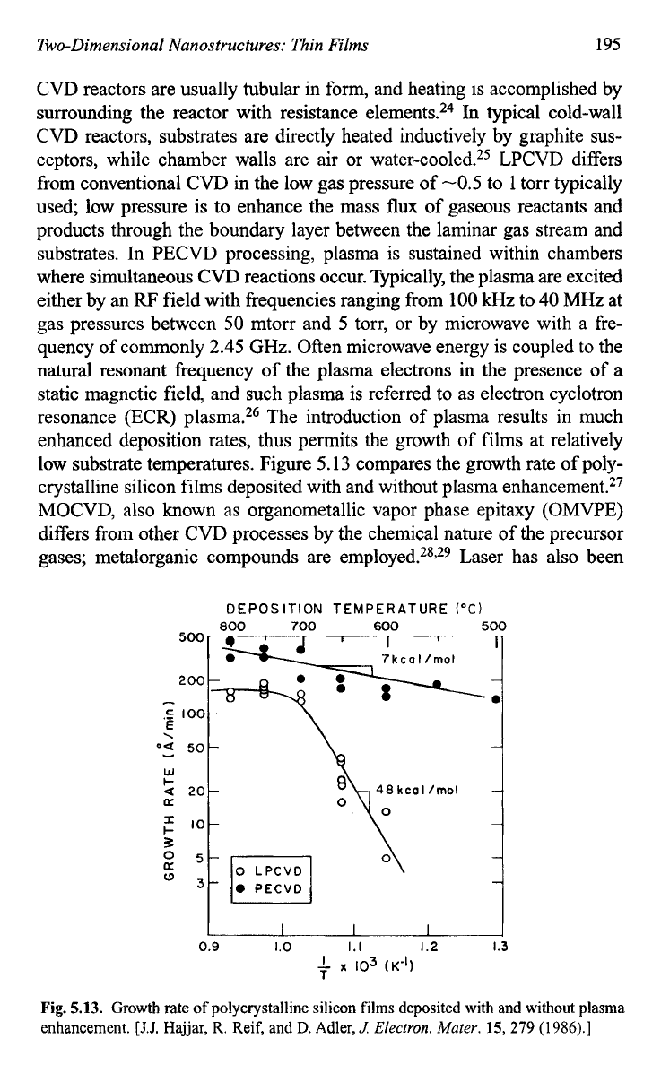
substrates. In PECVD processing, plasma is sustained within chambers
where simultaneous CVD reactions occur. Typically, the plasma are excited
either by an
RF
field with frequencies ranging from
100
kHz
to
40
MHz
at
gas pressures between
50
mtorr and
5
torr, or by microwave with a fre-
quency of commonly
2.45
GHz.
Often microwave energy is coupled to the
natural resonant frequency of the plasma electrons in the presence of a
static magnetic field, and such plasma is referred to as electron cyclotron
resonance (ECR) plasma.26 The introduction
of
plasma results in much
enhanced deposition rates, thus permits the growth of films at relatively
low substrate temperatures. Figure
5.13
compares the growth rate of poly-
crystalline silicon films deposited with and without plasma enhan~ement
MOCVD, also known as organometallic vapor phase epitaxy (OMVPE)
differs from other CVD processes by the chemical nature
of
the precursor
gases; metalorganic compounds are empl~yed?~.~~ Laser has also been
DEPOSITION
TEMPERATURE
("C)
1
I
I
1
I
0.9
1.0
1.1
I
.2
1.3
L
x
103
(~-1)
T
Fig.
5.13.
Growth rate
of
polycrystalline silicon films deposited with and without plasma
enhancement.
[J.J.
Hajjar,
R.
Reif, and
D.
Adler,
J
Electron.
Muter.
15,
279
(1986).]