Henini M. Handbook of Self Assembled Semiconductor Nanostructures for Novel devices in Photonics and Electronics
Подождите немного. Документ загружается.

Optical Properties of In(Ga)As/GaAs Quantum Dots for Optoelectronic Devices 89
from a single QD layer, with obvious implications for many device structures. For example, in
QD laser structures where lasing from the ground state is desired, the low gain from a single QD
layer can be overcome in part through long cavities and high refl ection coatings to reduce mirror
losses, but the most common method is to incorporate several QD layers. However, for this strat-
egy to be effective these layers must provide coincident gain. This is not straightforward since
growth of subsequent QD layers may be affected by the underlying layers, either by strain fi elds or
by changes in surface morphology resulting from the buried QDs. These effects place a limitation
on the minimum separation between layers and therefore the maximum number of QD layers
that can be accommodated within the active region of a laser. Transmission electron microscopy
(TEM) studies [32] have shown that a strong vertical correlation of QD layers occurs for separa-
tions of 20 nm or less. It was clear from this investigation that the QDs in the upper layers are
larger than those in the lower layers and this was confi rmed by scanning tunnelling microscopy
(STM) [33] . The increased size of QDs in subsequent layers of QD stacks has been attributed to
strain-induced In migration causing preferential QD nucleation above buried QDs. This reduces
the time taken to reach the critical thickness θ
crit
for the 2D–3D transition [34] and deposition
of the same amount of In will lead to larger QDs. In addition, In segregation from lower layers
[35] and enhanced In/Ga intermixing during capping [36, 37] is also possible. All these factors
can have a signifi cant effect on the emission energy and details of both redshifts [38–40] and
blueshifts [41–43] of emission compared with single layer structures have been reported.
Lower layer
Sample A
Upper
layer
1.00
1.05
1.10
1.301.25
1.20
1.15
Energy (eV)
PL intensity (a.u.)
PL intensity (a.u.)
Sample B
Sample D
Sample C
1.00
1.25
1.301.201.15
1.05
1.10
Energy (eV)
20
(c)
(a)
(b)
T 10 K
Ar
He-Ne
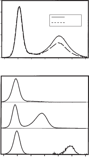
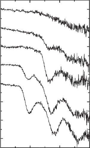
Figure 3.6 Low temperature (10 K) PL spectra obtained from samples containing two InAs/GaAs QD layers, sep-
arated by GaAs spacer layers of 40 nm (samples A and B), 20 nm (sample C) and 10 nm (sample D). Reprinted
with permission from Le Ru et al ., J. Appl. Phys. 9 1 , 1365 (2002) [44] , Copyright 2002, American Institute of
Physics.
CH003-I046325.indd 89CH003-I046325.indd 89 6/25/2008 12:33:59 PM6/25/2008 12:33:59 PM
90 Handbook of Self Assembled Semiconductor Nanostructures for Novel Devices in Photonics and Electronics
Figure 3.6 shows low temperature PL spectra obtained from samples containing two QD lay-
ers separated by GaAs spacer layers of different thickness [44] . The PL excitation intensity is low
(0.1 Wcm
2
) so emission from excited states is negligible. Both QD layers were grown under the
same conditions (by deposition of 2.3 ML InAs at a substrate temperature of 495°C) and are
separated by 40 nm (samples A and B), 20 nm (sample C) or 10 nm GaAs (sample D). For sam-
ples A and D, the GaAs spacer layer was grown at 495°C, the same temperature used for QD
growth, whereas the growth temperature for samples B and C was increased to 580°C after the
fi rst 10 nm GaAs. After the required GaAs thickness had been deposited the growth surface was
annealed under an As fl ux for 10 minutes. This annealing step desorbs segregated In from the
surface [45] and reduces surface undulations inferred from in situ refl ection high-energy electron
diffraction (RHEED) during growth. This was confi rmed by subsequent AFM studies of annealed
and unannealed GaAs surfaces [44] . The importance of the annealing step is illustrated in the
comparison of PL from samples A and B. For QDs grown on the unannealed surface, emission
is blueshifted, despite the large separation between layers. The higher energy peak at 1.20 eV
can be unambiguously assigned to emission from the second QD layer by excitation with either
an Ar
laser or an HeNe laser. The latter source penetrates deeper into the sample and gener-
ates a greater proportion of emission from the lower QD layer. In contrast, only a single peak is
observed from sample B, where the annealing step has successfully recovered a fl at GaAs surface.
As the separation between the QD layers is reduced to 20 nm (sample C), strain from the fi rst QD
layer affects growth of the second layer and emission is blueshifted, despite desorption of surface
In and smoothing of the GaAs surface by annealing. By reducing the separation between lay-
ers to 10 nm (sample D), the two QD layers become electronically coupled and strong emission
is detected only from the QDs in the fi rst layer, due to carrier redistribution to the lowest energy
QD states [38, 39] . For multiple QD-layer laser structures it is crucial to have the gain peak of all
layers coincident. A conclusion gained from the annealing study is that a spacer separation of
at least 40 nm is required for coincident emission. In order to determine whether the integrated
emission scales with the number of QD layers, two samples were compared; one consisting of a
single QD layer, the other containing three QD layers separated by 40 nm (annealed) GaAs spac-
ers. In order to avoid problems associated with carrier diffusion, a metal mask with apertures
60–210 μ m in diameter was deposited on the surface of each sample. A PL study then showed
unequivocally that the PL intensity obtained from the multiple QD layer sample was indeed three
times that observed from the single layer [44] . Thus, by following this recipe, coincident gain
from all layers is assured.
Electronically coupled QDs have attracted attention for structures designed to manipulate
either carrier charge or spin as qubits for quantum information applications and this is covered
more fully elsewhere in this book. For these applications it is desirable for the coupled QDs to be
identical; this is a considerable challenge for the reasons described above. In order to improve the
uniformity of QDs in a multiple layer structure, the so-called “ indium fl ush ” growth technique
can be used [45, 46] . QDs in each layer are partially capped by a thin layer of a few nm GaAs
before growth is interrupted and the substrate temperature is raised to desorb surface indium
before growth of the remaining GaAs spacer layer. This has the effect of truncating the QDs in
each layer so that they have the same height (although there may still be compositional varia-
tion between the QDs). In conclusion, self-assembled QDs require considerable growth expertise
to extract desirable optical properties for use in devices.
3.4 Energy states in QDs
The optical properties of a solid are dictated by the electronic structure; specifi cally the density of
states (DOS). As the dimensionality is reduced, the resulting modifi cation to the density of states
(DOS) is responsible for many of the improvements in the optical properties of QDs, including
higher material and differential gain, lower threshold current densities ( J
th
) in laser structures
[30] and even temperature insensitive operation (corresponding to a characteristic temperature
T
0
) [47] .
CH003-I046325.indd 90CH003-I046325.indd 90 6/25/2008 12:33:59 PM6/25/2008 12:33:59 PM
Optical Properties of In(Ga)As/GaAs Quantum Dots for Optoelectronic Devices 91
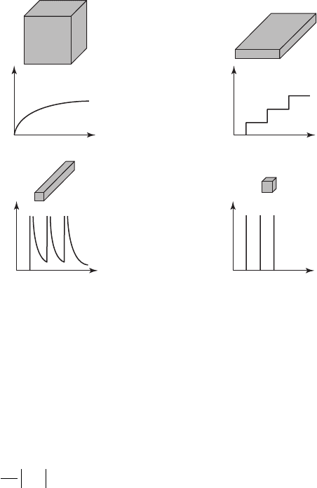
Figure 3.7 shows the conduction band DOS functions for systems with increasing confi ne-
ment. For bulk systems, the familiar g ( E ) α E
1/2
relationship is observed but for QWs, g ( E ) is con-
stant for each subband; for quantum wires with 2D confi nement g ( E ) is proportional to E
1 / 2
and for 3D confi nement a δ -function DOS is obtained. The most signifi cant aspect of this DOS
modifi cation is that an increased number of states are available near the band edge as confi ne-
ment is increased. The infl uence of the DOS is further illustrated by considering the probability of
an optical transition between two states as given by Fermi’s golden rule:
W
MgE
if if→
()
2
2
π
where W
i
→
f
is the transition rate between initial and fi nal states and M
if
is the optical matrix ele-
ment. Modifi cation of the DOS due to confi nement will increase the transition rate at the band
edge and the increased electron–hole overlap due to the spatial localization of carriers will
increase M
if
. The increased overlap will enhance the Coulomb interactions between the electron
and hole, forming excitons.
There have been many attempts at modelling the electronic states of QDs in the last ten years,
using a variety of methods. These include effective mass approximations [48] , 8-band k p theory
[49–51] and atomistic pseudopotential calculations [52] . These approaches rely on detailed knowl-
edge of the size, shape, composition and strain state of the QD. Numerous experimental approaches
have been used to determine these parameters, including STM [53, 54] , TEM [55–57] and X-ray
diffraction [58] , but it remains exceedingly diffi cult to completely determine the QD structure.
Early effective mass models for QDs with a shallow confi ning potential predicted a single bound
electron state and multiple hole levels [48, 59, 60] . These models were applied to optical emission
spectra obtained from QD ensembles that exhibited short wavelength emission and a large inho-
mogeneous broadening which masked the presence of excited state transitions. However, with
improvements in growth methods, QD samples with reduced inhomogeneous broadening were
realized and excited state emission was clearly observed [61] (see Figs 3.3 and 3.4 ). Itskevich et al.
showed that excited state transitions occur between electron and hole levels with the same quan-
tum number ( E
0
– H
0
, E
1
– H
1
, etc.) [62] , demonstrating that parity is a good quantum number.
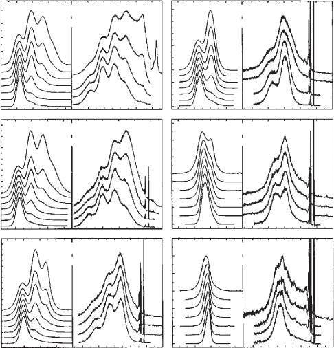
Figure 3.8 shows the results of applying pressure to a high-quality QD sample. With increasing
pressure there is a crossover between the conduction band Γ and X valleys and the optical transi-
tion becomes indirect. If only one electron state ( E
0
) is involved, PL emission from all the states
3D
(bulk)
g(E)E
1/2
g(E)E
1/2
g(E)d(E)
g(E)
g(E)
g(E) g(E)
g(E)
E
E
E
E
constan
t
1D
(quantum wire)
0D
(quantum dot)
2D
(quantum well)
Figure 3.7 Density of states (DOS) functions g ( E ) in quantum-confi ned systems.
CH003-I046325.indd 91CH003-I046325.indd 91 6/25/2008 12:34:00 PM6/25/2008 12:34:00 PM
92 Handbook of Self Assembled Semiconductor Nanostructures for Novel Devices in Photonics and Electronics
would quench simultaneously. However, the results showed that increasing pressure quenched the
optical transitions sequentially, showing that more than one electron state is present.
Use of multiple band k p or pseudopotential models allows a more rigorous simulation of the
QD energy levels, particularly regarding the strain state of the QD [49–52] . These approaches
predict the existence of multiple confi ned electron levels, consistent with excited state emis-
sion resulting from transitions between states of the same quantum number. They also lead to a
reduction of the error in the estimated excitonic band gap, which is signifi cantly overestimated
in some effective mass models [63] . Confi nement lifts the heavy-hole/light-hole degeneracy with
the hole ground state having predominantly heavy-hole character, although excited states may
be more mixed [64] and experimental evidence for the presence of pure light hole states in QDs is
inconclusive [65, 66] .
For these calculations structural (compositional) parameters must be assumed. Most models
consider a pyramidal QD of uniform In(Ga)As composition. Due to their increased effective mass,
hole wavefunctions are then expected to be confi ned towards the apex of the pyramidal QD, with
the electron wavefunction located towards the base. This would reduce the electron–hole over-
lap in the QD and so diminish the optical transition strength but would also result in a perma-
nent dipole in the QD. Measurements of the photocurrent with increasing applied bias for QDs in
p-i-n or n-i-p structures, shown in Fig. 3.9 , did indeed demonstrate the existence of a dipole, but this
was in the opposite direction to that expected for QDs of uniform composition, suggesting instead
that the hole is confi ned towards the base of the QD and the electron towards its apex [67] . This sug-
gests of a non-uniform InGaAs composition within the QD, with increasing In content towards the
top of the QD. This is borne out by STM [53] and X-ray diffraction measurements [58] . The compo-
sition gradient in QDs may be due to both indiffusion of Ga from the substrate during QD growth
[68] and In segregation [69] . Eight-band k p and pseudopotential calculations of InAs/GaAs QDs
2
2
2
2
2
2
2
2
2
2
3
3
3
3
3
3
3
4
4
4
4
1
1
1
1
1
1
1
1
1
1
1
1
5
GaAs
1.2 1.3 1.4 1.4 1.41.5 1.5 1.51.2 1.3 1.4 1.5 1.6 1.6 1.61.7
1.4 1.5
1.6 1.7
1.4 1.5
1.6 1.7
1.4 1.5
1.6 1.7
1.4 1.5
1.6 1.7
1.7 1.8
1.4 1.5
1.6 1.7 1.8
1.4 1.5
1.6 1.7 1.8
1.4 1.5
1.6 1.7 1.8
1.4 1.5
1.6 1.7 1.8
R
R
R
(b)
(c)
(f)
(a) (d)
(e)
R
R
Energy (eV)
P 65.1 kbar
P 60.1 kbar
P 49.5 kbar
P 38.8 kbar
P 54.7 kbarP 10.9 kbar
Intensity
Figure 3.8 PL spectra obtained from an InAs/GaAs QD sample at a range of excitation conditions (left panels:
10–300 Wcm
2
cw, right panels: 20–200 Wcm
2
pulsed) for increasing pressure, showing the effect of pressure
on QD states, labelled 1–5. Reprinted with permission from Itskevich et al ., Phys. Rev . B 60 , R2185 (1999) [62] ,
Copyright 1999 by the American Physical Society.
CH003-I046325.indd 92CH003-I046325.indd 92 6/25/2008 12:34:00 PM6/25/2008 12:34:00 PM
Optical Properties of In(Ga)As/GaAs Quantum Dots for Optoelectronic Devices 93
[70, 71] and InGaAs/GaAs QDs [72] which takes into account an increasing In content from the
bottom to the top of the QD do replicate the observed dipole orientation, with the hole wavefunction
confi ned at the base of the QD and the electron wavefunction confi ned towards the apex. These cal-
culations also demonstrate the sensitivity of the exciton emission energy to changes in In content,
with an increase in average In content of the QD from 50 to 60% resulting in a redshift of around
70 meV, while changes in the profi le of the In distribution of the QD redshift the emission by 20–
40 meV [72] . From studies of the Stark shift on emission from single InGaAs QDs, the magnitude of
the In:Ga composition gradient was found to be dependent on the In content of the QD [73] .
However, to a good fi rst approximation, QDs can be represented by a parabolic potential [74] ,
regardless of the details of the QD size, shape, composition and strain state. This is consistent
with the equal energy spacing between states seen in QD PL spectra (for example, in Fig. 3.3
and in [75] ) and by capacitance–voltage and far-infrared absorption measurements of InAs/
GaAs QDs determining the charging energies of the QD states [76] . For In(Ga)As/GaAs QDs, the
QD height is signifi cantly smaller than the QD diameter (especially once capped). By compari-
son with atomic systems, we would expect the electron ground state in a QD to be s-like with a
degeneracy of 2 (due to spin), and the fi rst excited state to be p -like with a degeneracy of 4. This
has been demonstrated in transmission experiments on InAs/GaAs QDs in a fi eld-effect structure
[77] , in which additional electrons were controllably added to the QDs (as shown in Fig. 3.10 ).
Absorption from the ground state of the QDs is quenched for an electron occupancy N
e
2 elec-
trons per QD, corresponding to a fi lled ground state. Absorption from the fi rst excited state is con-
siderably reduced at N
e
4 and completely quenched by N
e
6.
For PL emission resulting from interband recombination of electrons and holes, the energy
separation between the ground state (GS) and fi rst excited state (X1) PL emission represents the
sum of the electron level separation and the hole level separation. Typical GS–X1 separations
1.16
1.06
1.1
0.9
0.7
1.08
1.10
1.14
1.12
300 200
0 100
100
200 300
Electric field (kV/cm)
Oscillator strength
(arb. units)
Transition energy (eV)
T 200 K
C
C
(a)
(b)
B
B
D
A
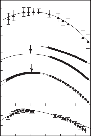
Figure 3.9 (a) Dependence of the peak photocurrent from the ground state (circles) and 1st excited state (triangles)
of QDs incorporated into p-i-n or n-i-p structures on applied electric fi eld, demonstrating the Stark shift of QD emis-
sion. The peak emission shift occurs for a negative applied fi eld, indicating the orientation of the dipole moment. (b)
Oscillator strength for the ground state transition of the QDs shown in curve BC in (a). Reprinted with permission
from Fry et al ., Phys. Rev. Lett . 84 , 733 (2000) [67], Copyright 2000 by the American Physical Society.
CH003-I046325.indd 93CH003-I046325.indd 93 6/25/2008 12:34:01 PM6/25/2008 12:34:01 PM
94 Handbook of Self Assembled Semiconductor Nanostructures for Novel Devices in Photonics and Electronics
in PL spectra are 50–70 meV, although this may be increased by variation of the QD growth
conditions [78–80] . The intraband separation between states in either the conduction band or
the valence band is not straightforward to determine experimentally, but experiments using far-
infrared (intraband) absorption to modulate near-infrared (interband) emission suggest typical
electron level separations of 45–55 meV and hole level separations of 10–15 meV [81, 82] , as
expected considering the greater effective mass for holes.
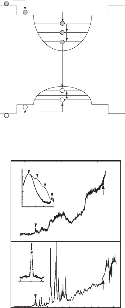
The traditional picture of carrier capture and relaxation processes in QDs is shown schemati-
cally in Fig. 3.11 . For most device applications, carriers are either electrically injected or optically
excited into the GaAs matrix surrounding the QDs (1). Carriers are then captured via the wet-
ting layer (WL) (2) into the QDs (3) and then rapidly relax to the ground state (4). Carrier cap-
ture and relaxation occurs on the order of ps. Once carriers reach the ground state ( E
0
), radiative
recombination may take place (5). Typical radiative lifetimes for carriers in QDs are around 1 ns.
If excitation or carrier injection is suffi cient for multiple carriers to be captured by each QD, state
fi lling can occur and radiative recombination may be observed from excited states. The discrete
energy levels restrict the number of energy states available for carriers in a QD, and this restric-
tion was predicted to severely inhibit carrier relaxation in QDs, since LO-phonon energies do
not match the energy separation between QD states (the so-called phonon bottleneck) [83, 84] .
This would have a major impact on device characteristics, for example gain recovery in lasers
and semiconductor optical amplifi ers. However, as mentioned above, carrier capture and relaxa-
tion in QDs is on the ps timescale [85, 86] . In order to circumvent the phonon bottleneck, effi -
cient carrier relaxation mechanisms via multiphonon processes [87] and by carrier–carrier
scattering [88, 89] have been proposed. Also the existence of 2D-like continuum states extend-
ing through the ladder of QD states to the ground state has been suggested [90] following photo-
luminescence excitation (PLE) measurements. As shown in Fig. 3.12 , PLE spectra obtained from
both QD ensembles ( Fig. 3.12a ) and from a single InGaAs/GaAs QD ( Fig. 3.12b ) show a rising
1.0004
1.0001
0.9998
0.9997
0.9999
1.0000
1.0002
1.0003
1.31.0 1.1 1.2
Ener
g
y (eV)
T(V
g
)/T(V
g
0.5 V)
N
e
1
N
e
0
N
e
6
N
e
4
N
e
2
Figure 3.10 Transmission spectra obtained from InAs/GaAs QDs in a fi eld-effect structure with increasing electron
occupancy ( N
e
) in the QDs, showing quenching of absorption as the QD states are fi lled. Reprinted with permission
from Warburton et al ., Phys. Rev. Lett . 79 , 5282 (1997) [77], Copyright 1997 by the American Physical Society.
CH003-I046325.indd 94CH003-I046325.indd 94 6/25/2008 12:34:02 PM6/25/2008 12:34:02 PM
Optical Properties of In(Ga)As/GaAs Quantum Dots for Optoelectronic Devices 95
1.3 1.35 1.4
ex>
Intensity (a.u.)
Intensity (a.u.)Intensity (a.u.)
1.2
1.3
1.4
WL band edge
WL band edge
(a)
(b)
Energy (eV)
1.281
1.282
Energy (eV)
100 150050
E
ex
E
det
(meV)
E
ex
(eV)
WL
1/40
Figure 3.12 (a) Far-fi eld PLE spectrum obtained from an InGaAs/GaAs QD ensemble with a detection energy
E
det
1.282 eV. The inset shows PL spectra obtained at low and high excitation powers from the same sample with
an excitation energy E
ex
1.959 eV. (b) Near-fi eld PLE spectrum obtained from a single InGaAs/GaAs QD; the inset
shows a PL spectrum obtained from the QD. Emission peaks due to an excitation energy E
ex
E
det
30 and 65 meV
are attributed to Raman scattering. Reprinted with permission from Toda et al ., Phys. Rev. Lett. 82 , 4114 (1999)
[90] , Copyright 1999 by the American Physical Society.
GaAs conduction band
GaAs valence band
WL
WL
E
2
E
1
E
0
H
0
H
1
H
2
1
4
2
3
5
Figure 3.11 Schematic diagram illustrating carrier capture from GaAs barrier into a QD via the wetting layer and
carrier relaxation within the QD .
CH003-I046325.indd 95CH003-I046325.indd 95 6/25/2008 12:34:02 PM6/25/2008 12:34:02 PM
96 Handbook of Self Assembled Semiconductor Nanostructures for Novel Devices in Photonics and Electronics
0 300250200150100
1.20
1.15
1.00
0.95
0.90
1.10
1.05
Ground state
1st excited state
InAs
Temperature (K)
50
45
40
10
20
30
35
0
5
15
25
1.00 1.05 1.151.10 1.20
Energy (eV)
1.8
1.6
0.2
0
0.4
0.8
0.6
1.2
1.4
1
10 K
300 K
PL intensity (a.u.)
PL intensity (a.u.)
(b)
(c)
(a)
0.90 0.95 1.00 1.05 1.10
Energy (eV)
Energy (eV)
Figure 3.13 (a) Temperature dependence of the GS and X1 peak emission from a sample containing a low density
(1.5 1 0
9
c m
2
) InAs/GaAs QD layer, with 10 K (b) and 300 K (c) spectra obtained from the sample. Also shown
in (a) is the temperature dependence of the InAs band gap energy, calculated from Varshni relations and then shifted
to match the QD GS transition at low temperature [104] .
background extending from an excitation energy 50 meV above the detection energy up to the
WL band edge due to these continuum states. Coupling between the continuum states and QD
states may provide an effi cient carrier relaxation mechanism, as carriers can easily relax through
the continuum states and then transfer to the QD ground state.
Consensus has not been reached regarding the origin of the continuum and its possible role in
QD carrier relaxation. It has been attributed to a band tail of deep states due to carrier localiza-
tion at the rough interfaces of the WL [91] or to be a result of crossed transitions between WL
valence band states and bound electron states in the QD [92, 93] . Coupling of the QD ground
state to the continuum states via LO-phonon emission provides a mechanism for carrier relaxa-
tion directly to the QD ground state rather than through the excited states, thus circumventing
the phonon bottleneck [94, 95] .
Alternatively, carrier relaxation in QDs may be infl uenced by the formation of polarons by
strong coupling of electrons [96–98] (or excitons [99] ) to LO-phonons. The polaron lifetime
(and thus the carrier relaxation) is expected to be determined by the lifetime of the LO-phonon
component [98, 100, 101] . Due to phonon anharmonicity, the LO-phonon component of the
polaron can relax by emission of two phonons [102] . The two-phonon emission can be of suf-
fi cient energy to match the separation between the electron states, allowing the electron to relax
between the states and circumventing the phonon bottleneck. However, polaron effects have
only been seen in samples where the electron–hole (Auger) relaxation method is not present, for
example in intraband measurements on n -doped QDs. If electrons and holes are present, Auger
scattering provides an effi cient mechanism for electron relaxation and the polaron mechanism
is not required [103] . For most devices, with high electron and hole densities, Auger scattering is
by far the most likely process for carrier relaxation.
The operating temperature of QD-based devices can vary signifi cantly depending on the appli-
cation. Conventional optical telecommunication devices such as lasers and SOAs are expected to
CH003-I046325.indd 96CH003-I046325.indd 96 6/25/2008 12:34:03 PM6/25/2008 12:34:03 PM
Optical Properties of In(Ga)As/GaAs Quantum Dots for Optoelectronic Devices 97
operate around room temperature or above (typically 20–80°C). Infrared photodetectors may be
expected to work with liquid nitrogen cooling at 77 K and novel devices such as QD single photon
sources have been demonstrated at low temperatures. However, the optical properties of QDs are
very different in these regimes, due to temperature dependent carrier capture and escape mecha-
nisms and the interplay between radiative and non-radiative processes.
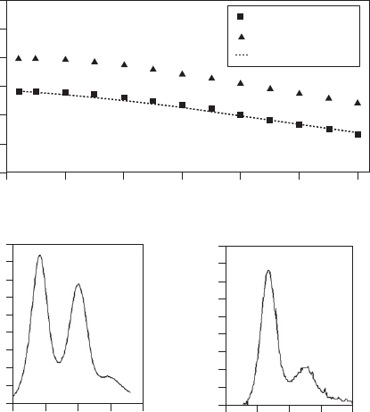
Figure 3.13a shows the temperature variation of the peak PL emission energy of the ground
state and fi rst excited state of an InAs/GaAs QD sample. The sample contains a single QD layer
with a very low QD density of 1.5 1 0
9
c m
2
. Thus signifi cant excited state emission is observed
even for moderate PL excitation power over the temperature range 10–300 K. As the temperature
is increased, the peak emission energy of both states redshifts, following a similar trend to that of
the InAs band gap [105–107] . In some cases, especially for samples exhibiting a large inhomoge-
neous broadening or a bimodal distribution of QDs, an increased redshift is observed for the QD
ensemble peak in the mid-temperature range (100–200 K), following a sigmoidal variation with
temperature [108, 109] . Figure 3.13 also shows 10 K (panel b) and 300 K (panel c) PL spectra
obtained from the sample. At 300 K, the PL intensity is reduced with respect to the low tem-
perature value by a factor of 20 due to the low QD density where carrier recapture is less likely.
A reduction in the PL intensity by a factor of 6 is seen in samples with higher QD density. Note
that the degree of state fi lling, as shown by the ratio of the ground state to fi rst excited state emis-
sion intensity, is also reduced due to thermal escape of carriers from the QDs.
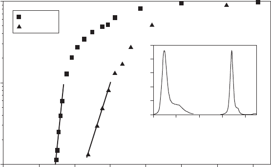
The temperature dependence of PL intensity from In(Ga)As/GaAs QDs is best described using
an Arrhenius plot, as shown in Fig. 3.14 , showing the integrated PL intensity (plotted on a loga-
rithmic scale) at various temperatures between 70 and 335 K (plotted as 1/ T or 1000/ T for rea-
sons outlined below) for two InAs/GaAs QD samples, A and B, obtained from the same epitaxial
wafer. Sample A contains as-grown InAs/GaAs QDs whereas sample B has been subjected to
post-growth rapid thermal annealing at 750°C for 10 s, which causes interdiffusion of In and Ga
in the QDs, blueshifting their emission energy and thus reducing the potential barrier height for
carrier escape to the WL or GaAs matrix [110] . Note that the QD density in both samples is the
same. The PL spectra were obtained using a low excitation density of 4 W c m
2
, and the contri-
bution of excited state emission is small.
Sample A
Sample B
1
0.01
0.1
02468101214
1000/T(K
1
)
Integrated PL intensity
PL intensity (a.u.)
10 K
Sample
Sample
AB
1.00
1.10
1.20
1.30
1.40
Energy (eV)
E
a
483 meV
E
a
142 meV
Figure 3.14 Arrhenius plot of the temperature dependence of PL intensity from InAs/GaAs QD samples with dif-
ferent confi ning potentials. Inset : 10 K PL spectra obtained from the two samples.
Three regimes can be identifi ed in the Arrhenius plots: (1) at low temperatures ( 100 K for
the QDs presented in Fig. 3.14 ) the integrated PL intensity from the QDs remains constant, (2) at
CH003-I046325.indd 97CH003-I046325.indd 97 6/25/2008 12:34:04 PM6/25/2008 12:34:04 PM
98 Handbook of Self Assembled Semiconductor Nanostructures for Novel Devices in Photonics and Electronics
high temperatures the PL intensity is strongly quenched with increasing temperature, following
a dependence of the form:
IC EkT
aB
exp
()
where E
a
is an activation energy for carrier escape from the QDs, and (3) at intermediate temper-
atures the PL intensity starts to drop but does not immediately follow the exponential quenching
behaviour. This mid-temperature range coincides with the sigmoidal variation of the PL emis-
sion energy mentioned above and also with a narrowing of the PL linewidth that is frequently
observed [109, 111–113] . These effects are attributed to a redistribution of carriers from small
QDs on the high-energy side of the QD spectral distribution to larger, low-energy QDs, due to
preferential thermal escape from the small QDs with lower potential barrier height.
From the gradient of the Arrhenius plot at high temperatures, the activation energy E
a
can be
determined, which is in good agreement with the difference between the GaAs band gap and the
QD ground state energy ( E
a
E
GaAs
E
QD
) [114] . The quenching of the PL is attributed to non-
radiative recombination of carriers in the GaAs barrier [115] .
The temperature dependence of PL intensity (normalized to have the same integrated inten-
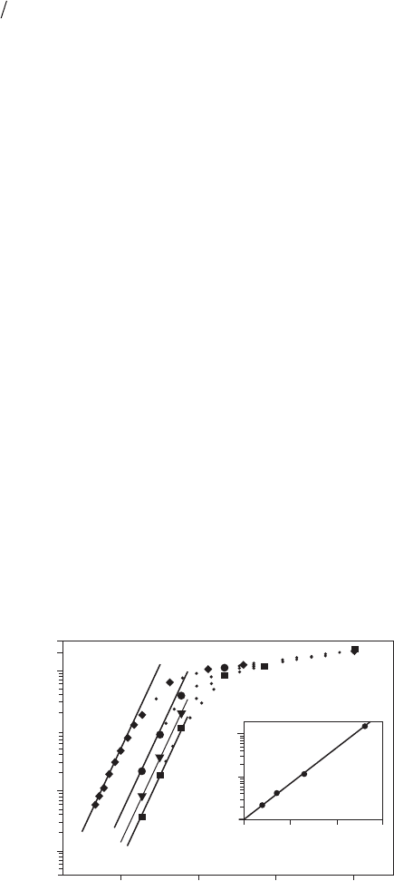
sity at 10 K) from an InAs/GaAs QD sample at different excitation powers is shown in Fig. 3.14
[114] . The excitation density is varied between 25 mWcm
2
and 4 Wcm
2
, and is low enough
such that excited state emission can be neglected. From the gradients of the fi t lines at high
temperatures, a common activation energy E
a
270 meV is obtained for all excitation powers,
as expected. However, as the excitation density is reduced, quenching of the PL intensity occurs
at lower temperatures. This suggests that at higher temperatures ( 150 K), the regime where
carrier escape is observed, the excitation dependence of the PL intensity becomes superlinear.
The inset to Fig. 3.15 shows that C follows a quadratic dependence with the PL intensity I ( P ).
If the excitation density is further increased so that the average carrier occupancy of the QDs
is greater than one electron–hole pair per QD, the dependence changes to a linear one: I ( P ) α P
[114] . This behaviour is attributed to the independent capture and escape of electrons and holes
in QDs: for low excitation, with an average QD occupancy of less than one electron–hole pair per
QD, the probability of capture and one electron and one hole by a QD (necessary for PL emission)
will depend quadratically on the excitation power. This illustrates the importance of the statistical
nature of carrier capture and escape in QD ensembles: the carrier distribution across the ensemble
Integrated PL (I/I
0
)
E
a
270 meV
1000/T(K
1
)
46810
100.1 10.01
C(P) P
1.9
C(P)
P (W cm
2
)
Figure 3.15 Arrhenius plots of the temperature dependence of PL intensity (normalized at 10 K) from an InAs/
GaAs QD sample for a range of excitation levels: 25 mWcm
2
(squares), 50 mWcm
2
(triangles), 0.2 Wcm
2
(cir-
cles) and 4 Wcm
2
(diamonds). Fit lines at high temperature are used to extract the activation energy, E
a
, and coeffi -
cient of the exponential, C. Inset : Dependence of C on excitation power. Reprinted with permission from Le Ru et al .,
Phys. Rev. B 67 , 245318 (2003) [114], Copyright 2003 by the American Physical Society.
CH003-I046325.indd 98CH003-I046325.indd 98 6/25/2008 12:34:04 PM6/25/2008 12:34:04 PM