Henini M. Handbook of Self Assembled Semiconductor Nanostructures for Novel devices in Photonics and Electronics
Подождите немного. Документ загружается.

Optical Properties of In(Ga)As/GaAs Quantum Dots for Optoelectronic Devices 109
reducing the strain experienced by the QDs in the structure. A similar approach has also been
reported in achieving long wavelength (1450 nm) lasing at room temperature from a tunnel
injection laser [196] , in which QD layers are electronically coupled to a QW. This broad area
(1 mm 8 0 μ m) device, containing six coupled QW–QD layers and with high-refl ectivity facet
coatings, exhibits a remarkably low room temperature J
th
6 3 A c m
2
, despite use of the meta-
morphic buffer.
3.7 Vertical and resonant cavity structures
One of the advantages of QD growth on GaAs substrates is the ability to include distributed Bragg
refl ectors (see Fig. 3.5 ) into structures to limit the number of photon modes that can couple to the
QDs. Al(Ga)As/GaAs DBRs have a large refraction index contrast such that high refl ectivities can be
achieved with a modest number of periods. Electrical injection is complicated by the high diffusivity
of Be (the most common p -dopant in MBE-grown GaAs) towards the GaAs/AlAs interfaces which
results in large series resistances. This problem can be overcome through the use of C doping although
the high operating temperature of C-cells make them more diffi cult to control than Be cells.
40
30
0
1100 1200 1300
20
10
Substrate
DBR
QD layer
TiAu/contact
Power spectral density (a.u.)
(ii)
(i)
5
(nm)
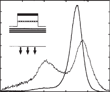
Figure 3.24 Power spectral density of a QD RCLED. The structure is designed for substrate emission. Excited state
emission is inhibited by the cavity and the useful light coupled to a fi bre below the substrate is increased by a factor of
10 compared with the control (no DBR). From Gray et al ., Electron. Lett. 35 , 242 (1999) [28] .
A schematic of a QD resonant cavity–LED (RC–LED) structure is shown in Fig. 3.24 . A sin-
gle layer of QDs is incorporated in a λ -cavity consisting of a lower AlGaAs/GaAs DBR and an
upper Ti/Au contact which acts as the top mirror (avoiding the problem of growing a p -doped
DBR) [28] . The cavity resonance is broad since the DBR mirror refl ectivity is constrained to allow
substrate emission, but excited state emission is arranged to lie outside the stop band. Although
there is imperfect matching of the cavity resonance and the QD GS emission, a comparison with
the control sample (no DBR) demonstrates a factor of ten improvement in the coupling to an opti-
cal fi bre butted against the substrate. QD resonant cavity photodiodes for detection at 1300 nm
[197] or 1060 nm [198] have also been reported where the top mirror was an MgF/ZnSe DBR.
These devices had a reported detection effi ciency of 49% and 65%, respectively, with extremely
small spectral bandwidths 2 n m .
Vertical cavity surface emitting lasers (VCSELs) incorporate one or more layers of QDs between
two DBRs. Their low excitation volume means they are low-power devices with high directionality
CH003-I046325.indd 109CH003-I046325.indd 109 6/25/2008 12:34:12 PM6/25/2008 12:34:12 PM
110 Handbook of Self Assembled Semiconductor Nanostructures for Novel Devices in Photonics and Electronics
10
20
30
80
70
60
50
40
1272 1278 1280 12821274 1276
Wavelength (nm)
4 mA
1.6 mA
1.6 mA
2 mA
3.8 mA
2.6 mA
4 mA
3.2 mA
Intensity (dBm)
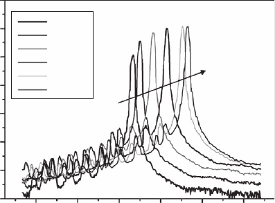
Figure 3.25 Lasing from a QD VCSEL. Note the low operating current (threshold 7.6 kAcm
2
). A T
0
450 K was
measured for this device. From Chang et al ., IEEE Photon. Technol. Lett. 18 , 847 (2006) [204] , © 2006 IEEE.
and high-temperature emission wavelength stability. Relatively few studies have been made
on QD VCSELs and most devices operate at wavelengths of 1000 nm or less [29, 199–203] ,
although 980 nm is a target wavelength for short distance optical interconnects. Recently,
1300 nm versions have been demonstrated [204–206] as shown in Fig. 3.23 . This device uses
C-doping and contains fi ve QD layers in a 3 λ /2 cavity. In order to confi ne the injected current to
the centre of the structure (in this case a 26 μ m mesa) the AlGaAs layers are deliberately oxidized
to allow current only within a 5 μ m central region. This technique is commonly used to lower
the threshold current of VCSELs by producing a layer of Al
2
O
3
between the cavity layer and one
of the Bragg refl ectors using a steam environment at 350 to 500°C. The rate of formation of the
oxide layer is proportional to the content of Al in the material; thus the oxide forms fi rst in those
layers with the highest Al content. The refractive index of the oxide layer is lower than that of the
semiconductor and also acts as a waveguide for the emitted light. Although this is an impressive
result it is not clear that such devices can become commercially viable.
3.8 Semiconductor optical amplifi ers
As the speed of data communications increases, regeneration (amplifi cation) of optical pulses by
conversion to electrical signals becomes increasingly diffi cult and optical amplifi ers are seen as the
key to “ all optical ” networks. The erbium doped fi bre amplifi er has been one of the major innova-
tions in optical communications but is confi ned to the 1550 nm wavelength range where attenua-
tion is already low. Developments of fi bre amplifi ers (doped with praseodymium) for the 1300 nm
range have been slow and considerable effort has been put into semiconductor optical amplifi ers
(SOAs) having bulk or QW active regions. SOAs are essentially laser diodes without end mirrors
and are frequently called travelling wave amplifi ers. To prevent laser oscillation (which results
in ripples in the gain spectrum) the facets can be antirefl ection coated ( R 0.001%) or a tilted
waveguide geometry can be used. At present QW SOAs are available from 850 to 1600 nm utiliz-
ing GaAs- and InP-based materials systems and can provide up to 30 dB of gain. Figure 3.26a
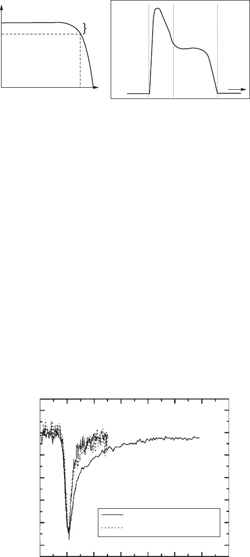
shows how the gain of an SOA decreases as the input signal power increases. Carrier depletion
leads to gain saturation and this can cause signifi cant signal distortion, as shown in Fig. 3.26b .
This is known as the pattern effect. If the gain change is too slow to follow the signal level tran-
sient, which is the case for conventional SOAs, or if the bit rate is high, the output waveform is
distorted as shown on the right part of the diagram.
The gain recovery in conventional bulk and QW SOAs exhibits two characteristic time constants;
a short one (subps) which arises from strong non-linear effects such as spectral hole burning
CH003-I046325.indd 110CH003-I046325.indd 110 6/25/2008 12:34:12 PM6/25/2008 12:34:12 PM
Optical Properties of In(Ga)As/GaAs Quantum Dots for Optoelectronic Devices 111
and subsequent fast intraband scattering, and a longer one of order 100 ps which is attributed
to slow carrier refi lling by current injection and diffusion. QD SOAs offer ultrafast (zero pattern
effect) non-linear gain recovery nearly an order of magnitude faster than QWs or bulk material
(see Fig. 3.27 ) with amplifi cation at bit rates of 40–160 Gbits [207] and a spectrally broad gain
(fast temporal response) giving them distinct advantages over their bulk and QW counterparts. In
addition, 1300 nm operation on a GaAs substrate makes these devices commercially very attrac-
tive. A problem for single pass travelling wave SOAs is the relatively low gain. Although many QD
layers can be incorporated into the active region a 20 dB gain will require devices longer than
5 mm.Bulk and QW SOAs are polarization sensitive due in part to the waveguide geometry but
also to the valence band symmetry. Recently, polarization insensitivity has been demonstrated in a
QD SOA through close stacking of many dot layers to form a columnar dot structure [208] .
Finally, it should be noted that SOAs exhibit signifi cant non-linear effects due to a changing
carrier population during operation. These can cause problems such as frequency chirping and
cross-modulation of signals. However, these can be put to advantage in the generation of new
frequencies due to four wave mixing (FWM). This is a coherent non-linear process that mixes a
pump beam of frequency ω
0
with that of a signal beam of frequency ω
0
Ω to generate a con-
jugate signal at ω
0
Ω as shown in Fig. 3.28 [141, 143] . Such optical wavelength converters
will play a crucial role in all optical networks. Thus a combination of large bandwidth gain and
A
B
P
out
(dB)
Gain (dB)
(a)
(b)
t
3 dB
Figure 3.26 Gain saturation due to carrier depletion (a) leads to distortion (pattern effect) in the output pulse. If
the bit rate is lower than the gain recovery the leading part of the pulse (part A) is amplifi ed with unsaturated gain,
but the trailing part (B) is distorted.
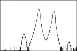
0.2
0.0
0.2
101 45623
0.4
0.8
0.6
Gain change (dB)
bulk (0.14)
0.25 mm, 120 mA
QD 0.475 mm, 20 mA
QD 1.01 mm, 12 mA (1.24)
Delay (ps)
Figure 3.27 Comparison of the gain compression dynamics of a QD (at two current inputs) and a bulk InP-based
SOA. The gain recovery is some seven times faster for the QD device. From Bimberg and Ribbat, Microelectron. J.
34 , 323 (2003) [206] .
CH003-I046325.indd 111CH003-I046325.indd 111 6/25/2008 12:34:13 PM6/25/2008 12:34:13 PM
112 Handbook of Self Assembled Semiconductor Nanostructures for Novel Devices in Photonics and Electronics
wavelength range, fast recovery and polarization insensitivity should provide an alternative to
QW SOAs in future fi bre networks.
3.9 Single photon sources
Single photon sources are attractive for a variety of applications, including metrology [209] ,
quantum key distribution [210] and linear optical quantum computing [211, 212] . Single pho-
ton emission has been demonstrated from a variety of sources, including single molecules [213,
214] and colour centres in crystals, for example nitrogen vacancies in diamond [215–217] , and
also from QDs [218–220] . QDs are particularly attractive as single photon sources because they
can be incorporated into standard optoelectronic device structures allowing electrical operation
of the source and integration into optical fi bre communication systems. As mentioned earlier,
typical growth conditions yield QD ensembles with QD densities of 10
10
c m
2
(100 μ m
2
).
However, in order to isolate single QD emission in practical device structures a QD density
approaching 10
8
c m
2
( 1 μ m
2
) is required – two orders of magnitude less than for normal
growth conditions. Growth on patterned substrates has been shown to result in low QD densities,
by preferential QD nucleation at nanoholes [221] or growth of InGaAs QDs embedded in GaAs/
AlGaAs pyramidal structures [222] , and single photon emission has been observed from QDs
grown by both of these methods [222, 223] . Alternatively, it is possible to signifi cantly reduce
the QD density on conventional substrates through accurate control of growth conditions, for
example by reduction of the InAs QD growth rate.
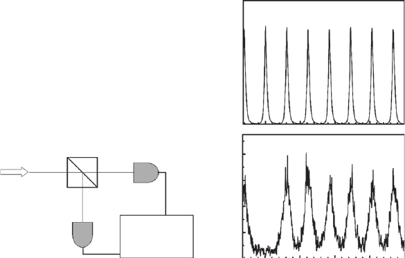
The standard method for evaluating a single photon source is to perform a correlation meas-
urement following the Hanbury–Brown and Twiss (HBT) experiment [224] , as shown in Fig.
3.29a . Emission from the source is incident on a beam-splitter and directed to one of two pho-
todetectors and the time delay ( τ ) between detection events is evaluated. From the correlation
between detection events, a second-order correlation function g
(2)
( τ ) is obtained which estab-
lishes the nature of the light source [209] . Attenuated laser sources (such as those currently
used in commercial quantum cryptography systems) are Poissonian sources, i.e. the probability
of a light pulse from the source containing n photons follows a Poissonian distribution P ( n ). This
results in a constant g
(2)
( τ ) 1. However, for an ideal single photon source g
(2)
(0) 0, since the
single photon from the source must be directed by the beam-splitter to one or other of the detec-
tors and simultaneous detection events are impossible.
Single photon emission from QDs relies on the cascade emission process [225, 226] . Due to
Coulomb interactions, the biexciton emission energy is spectrally shifted with respect to the sin-
gle exciton. As carriers are captured, relax and recombine in a single QD, emission will be char-
acterized by multiple exciton complexes until the fi nal electron–hole pair recombines at the
exciton energy (which can be spectrally resolved). HBT correlation measurements of the exci-
ton emission demonstrate photon antibunching ( g
(2)
(0) 1) [218, 225] and cross-correlation
measurements using a modifi ed HBT set-up (in which monochromators are used so that one
0
20
1150 1160 1170 1180 1190
40
80
60
Wavelength (nm)
Power (dB)
Signal
Pump
Conjugate
Figure 3.28 Wavelength conversion by four-wave mixing of a pump and signal beam in a QD SOA. Reprinted with
permission from Akiyama et al. , Appl. Phys. Lett. 77 , 1753 (2000) [141] , Copyright 2000, American Institute
of Physics.
CH003-I046325.indd 112CH003-I046325.indd 112 6/25/2008 12:34:14 PM6/25/2008 12:34:14 PM
Optical Properties of In(Ga)As/GaAs Quantum Dots for Optoelectronic Devices 113
photodetector will detect emission from the biexciton and the other detects emission from exciton
recombination) demonstrate conclusively that sequential emission of the biexciton then the exci-
ton occurs [226] .
For a practical single photon source it is advantageous to place the QDs within a microcavity
in order to increase the photon extraction effi ciency. Although a QD single photon source that
does not utilize a microcavity structure has been demonstrated [220] , the high refractive index
of GaAs ( 3.5) results in a low critical angle for total internal refl ection at the GaAs/air inter-
face and so only a small fraction of photons emitted from the QD will escape the device. Placing
the QDs within a planar microcavity structure, with a DBR mirror below the QD layer, has been
shown to improve the photon collection by a factor of ten [227] . Further modifi cation of the
microcavity design by introducing lateral confi nement of the optical modes, for example by using
micropillars [228, 229] , microdisks [230] or photonic crystal cavities [231, 232] , can result
in considerable alteration in emission from QDs, with signifi cant enhancement of spontaneous
emission into a cavity mode due to the Purcell effect [233] . The spontaneous emission rate from
InAs/GaAs QDs has been enhanced by fi ve times when the QDs were incorporated into a micro-
pillar and by 15 times when the QDs were incorporated in a microdisk [230] . Considering micro-
pillars, the spontaneous emission coupling coeffi cient β , the fraction of spontaneous emission in
a single cavity mode, increases with decreasing pillar diameter, and values as high as β 0 . 7 8
have been reported for a 0.5 μ m diameter micropillar [234] . Effi cient coupling of the spontaneous
emission into a cavity mode in this manner should improve the overall effi ciency of single photon
sources. However, the extraction effi ciency may be reduced for small micropillar diameters (less
than 3 μ m) as scattering due to the roughness of the etched sidewalls becomes signifi cant, caus-
ing deterioration in the cavity Q -factor [235] . The overall effi ciency of the single photon source
is also dependent on the collection optics of the system; if the numerical aperture of the collec-
tion optics is less than 1 then overall extraction effi ciencies from small cavity diameters may be
reduced. This places a limitation on the optimum micropillar cavity diameter to around 1–2 μ m.
Single photon emission from a single InAs/GaAs QD in a 1.9 μ m diameter pillar microcavity with
a photon collection effi ciency of 10% has been demonstrated [236] . This further emphasizes the
requirement for a very low QD density ( 10
8
c m
2
) in order to isolate a single QD in a QD single
photon source device structure.
(a) (b)
Emission
Beam-splitter
Detector
Detector
Correlator
B Exciton transition (1X)
A Ti:sapphire laser
80
80
60
60
0
0
40
40
20
20
Time t (ns)
G
(2)
(t)
G
(2)
(t)
Figure 3.29 (a) Schematic diagram of the Hanbury–Brown and Twiss experiment. (b) Correlation functions
g
(2)
( τ ) obtained from a pulsed Ti:sapphire laser (A), representing a Poissonian source, or from the exciton transition
of a QD (B), for which there is suppression of the correlation signal at zero delay τ 0. Part (b) from Michler et al. ,
Science 290 , 2282 (2000) [218] .
CH003-I046325.indd 113CH003-I046325.indd 113 6/25/2008 12:34:15 PM6/25/2008 12:34:15 PM
114 Handbook of Self Assembled Semiconductor Nanostructures for Novel Devices in Photonics and Electronics
Currently the majority of QD single photon sources that have been demonstrated operate at
wavelengths 1000 nm, mainly for compatibility with Si-based detectors. For integration with
optical fi bre-based telecommunications systems, emission at 1300 or 1550 nm is desirable.
Single photon emission at 1300 nm has been demonstrated from single InAs/InP QDs [237] but
this material system is not suitable for incorporation into micropillar structures due to the lack of
high-quality DBR mirrors. In order to extend low temperature emission from low density InAs/
GaAs QDs to 1300 nm, two approaches have been reported. The fi rst method uses bimodal QD
ensembles grown under conditions so that there is a very low density of large, long-wavelength
QDs, along with a higher density of smaller QDs (emission from these small QDs can be spectrally
fi ltered). These QDs have been incorporated into micropillar structures and single photon emis-
sion from the devices has been observed [238] . Alternatively, low density InAs/GaAs QDs can be
grown using very low InAs growth rates. As the growth rate is reduced the resulting QD density
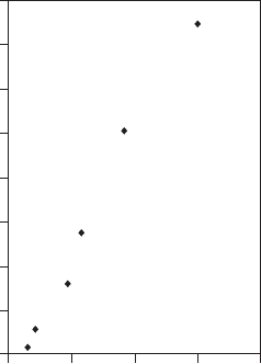
is also reduced, with a concomitant increase in QD size [239] . Figure 3.30 shows the variation of
InAs/GaAs QD density as the InAs growth rate is reduced. If the growth rate is reduced to these
very low levels, a QD density of 10
8
c m
2
can be achieved [240] .
160
140
80
0
0 0.015 0.020.005 0.01
60
20
40
120
100
Growth rate (MLs
1
)
QD density (10
8
cm
2
)
Figure 3.30 Variation of QD density in InAs/GaAs QD samples grown at a substrate temperature of 500°C at
low growth rates.
As the growth rate is reduced and the resulting QD size is increased, the QD emission wave-
length is extended but saturates at around 1200 nm at 10 K for GaAs-capped QDs [9] . However,
by capping the QDs with InGaAs, extension of the low-temperature emission of the QDs to beyond
1300 nm can be achieved [240] . These QDs have been incorporated into planar microcavities and
antibunching of the exciton emission from single QDs has been observed [241] . Very recently the
fi rst electrically-driven QD single photon source operating near 1300 nm was demonstrated [242] .
3.10 Entangled photon sources
There has been growing interest in extending the concept of the QD single photon source to real-
ize polarization-entangled photon sources, for quantum information applications including alter-
native key distribution methods in quantum cryptography [243] . This requires photons from the
source to be indistinguishable [244, 245] . By a photon interference experiment, Santori et al.
have shown that consecutive photons from an InAs/GaAs QD micropillar single photon source
were indeed indistinguishable [246] and this has been used to generate polarization-entangled
photon pairs using post-selected photons from the source [247] . This method of entanglement
CH003-I046325.indd 114CH003-I046325.indd 114 6/25/2008 12:34:15 PM6/25/2008 12:34:15 PM
Optical Properties of In(Ga)As/GaAs Quantum Dots for Optoelectronic Devices 115
utilizes just the exciton emission from the QD single photon source, but the cascade emission
process in QDs can provide sequential emission from the biexciton and then the exciton [226]
and it has been proposed that this can produce pairs of entangled photons [248] .
Following this proposal, we assume the polarization of the emitted photons is due to selection
rules discussed in more depth in the next section on spintronics. The biexciton comprises two
electrons with spin J
z
1/2 and two heavy holes with spin J
z
3/2. For bright transitions
where Δ J 1 then according to the selection rules the emitted photon will have positive or nega-
tive circular polarization σ
or σ
. Assuming there is no spin-fl ip during the cascade process then
the fi rst photon emitted will have a polarization of σ
or σ
and the photon resulting from the
second exciton recombination will have the opposite polarization; so the two-photon state should
be entangled, as described by:
ψσσσσ
1
2
12 12
()
To achieve entanglement the two decay paths, as shown in Fig. 3.16 earlier, must be indistin-
guishable. First reports showed emission of classically correlated photon pairs from the biexci-
ton cascade, illustrating a clear relationship between the polarization of the two photons, but not
entanglement [249, 250] . This is attributed to the lifting of the spin degeneracy due to asym-
metry of the QD resulting in fi ne structure splitting, as discussed previously. The fi ne structure
splitting presents a major obstacle to the realization of entangled photon sources based on the
biexciton–exciton cascade process because the two photons can now be distinguished according
to the sequence of the exciton recombination (which decay path was taken). Entanglement has
been achieved using photons from the biexciton cascade in QDs with fi ne structure splitting, but
only by spectral fi ltering to post-select photons from a spectral region where emission from the
two exciton polarizations overlap [251] . In order for the photons to be indistinguishable, the fi ne
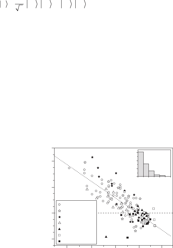
structure splitting must be less than the homogeneous linewidth [252] . Numerous approaches
have been taken in order to control the fi ne structure splitting. One is to compensate for the
asymmetry in the QD by applying an external lateral electric [253, 254] or magnetic fi eld [255] ,
or by applying a uniaxial stress along the [110] crystal direction [256] . Alternatively, post-
growth annealing of the QDs can be used to tune the fi ne structure splitting [128, 252, 257,
258] . The splitting follows a broadly linear trend with the emission energy, as shown in Fig. 3.31 ,
passing through zero fi ne structure splitting at around 1.4 eV, which also matches a similar trend
No anneal
650°C 5 min
650°C 10 min
700°C 5 min
700°C 15 min
750°C 5 min
750°C 10 min
80
40
40
0
1.34 1.36 1.38 1.421.4
X recombination energy (eV)
30
20
10
0
04
8
12
Frequency
S error (eV)
Exciton level splitting S (eV)
Figure 3.31 Fine structure splitting from single InGaAs/GaAs QDs under various annealing conditions. Inset :
Histogram of errors in the fi ne structure measurements. Reprinted with permission from Young et al. , Phys., Rev. B
72 , 113305 (2005) [128] , Copyright 2005 by the American Physical Society.
CH003-I046325.indd 115CH003-I046325.indd 115 6/25/2008 12:34:16 PM6/25/2008 12:34:16 PM
116 Handbook of Self Assembled Semiconductor Nanostructures for Novel Devices in Photonics and Electronics
from unannealed QDs of different sizes [259] . The reduced (and zero) fi ne structure splitting in
these shallow QDs is attributed to a reduction in the piezoelectric effect that causes the electron
and hole wavefunctions to point in orthogonal directions.
By selecting QDs with emission around 1.4 eV and negligible fi ne structure splitting, recent
experiments have now demonstrated entanglement of photons from the biexciton cascade [260,
261] . Prospects for a QD-based entangled photon source at longer wavelengths are currently
low, although very few studies have considered QDs emitting at these wavelengths [262, 263] .
Indirect measurements of InAs/GaAs QDs emitting at 1260 nm at 7 K suggest a fi ne structure
splitting of 20–90 μ eV [262] , although STM studies of InGaAs-capped QDs suggest that these
QDs may be much more symmetric than similar GaAs-capped, because preferential In migration
out of the QD along the [
110
] direction during capping is inhibited by the InGaAs cap [264] .
3.11 Spin-LEDs and the potential for QDs in spintronic devices
Exploitation of the spin of carriers in semiconductor devices is currently the focus of consider-
able research interest. The use of carrier spin in addition to charge may result in improvement in
device performance [265] and development of new types of devices including non-volatile mem-
ory devices and the use of the spin of nuclei or carriers as information bits in quantum comput-
ing ( “ qubits ” ) [266, 267] .
Research concerning spin in semiconductors focuses on development of magnetic materials, spin
injection into semiconductors and subsequent spin transport, manipulation and detection. One type
of device that is useful to evaluate spin injection from magnetic materials into semiconductor device
structures is the spin-light-emitting diode (spin-LED) [268–270] , where electrical injection of car-
riers from a magnetic contact or through a layer of magnetic semiconductor gives a spin-polarized
population of carriers, which then radiatively recombine in the active region of the LED. The polar-
ization of the emitted light can then be related to the spin of the carriers from radiative selection
rules. For a useful spin-LED, we require effi cient transfer of injected spin to the LED active region and
subsequent carrier relaxation and radiative recombination with the minimum of spin relaxation.
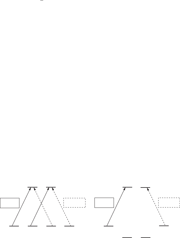
The radiative selection rules apply to both absorption and emission of light. The selection rules
for absorption of circularly polarized light in bulk GaAs are illustrated in Fig. 3.32a . Excitation by
circularly polarized light introduces a net spin polarization of the photo-excited electrons, with a
maximum of 50% net spin polarization, since both heavy and light hole states are excited but
heavy hole transitions are favoured by a ratio of 3:1 [271] . In strained semiconductors or for
low-dimensional systems, the degeneracy of the valence band may be lifted and the spin polari-
zation thus increased, since excitation will now involve one type of hole state, as in Fig. 3.32b .
J
z
J
z
Conduction band1/2 1/2
1/2
1/2
1/2
1/2
1/2
1/2
3/2
3/2
3/2
3/2
3
31
1
hh
hh
hh
hh
1h 1h
1h
1h
Valence band
(a)
(b)
Figure 3.32 Polarization selection rules for absorption of circularly polarized light into (a) bulk, unstrained GaAs
(numbers by the arrows represent the relative transition strengths). (b) A strained and/or low dimensional system
where the degeneracy of the heavy and light hole states has been lifted.
CH003-I046325.indd 116CH003-I046325.indd 116 6/25/2008 12:34:17 PM6/25/2008 12:34:17 PM
Optical Properties of In(Ga)As/GaAs Quantum Dots for Optoelectronic Devices 117
As shown above, in bulk GaAs around the Γ -point the heavy and light holes are mixed and
this leads to very rapid spin relaxation of holes, so in the majority of cases it is the electron spin
that is exploited. The dominant spin relaxation mechanism in undoped bulk III–V semiconduc-
tors, especially at low temperature, is the D’yakanov–Perel mechanism [271] . This arises because
in III–V semiconductors there is no centre of symmetry in the unit cell (so-called bulk inversion
asymmetry), which leads to a lifting of the degeneracy of the conduction band spin states, equiv-
alent to applying a small magnetic fi eld. If the direction of motion of the electron differs from the
direction of this effective magnetic fi eld, precession of the electron will lead to spin relaxation.
However, in QDs, since there is 3D confi nement of the electron, the D’yakonov–Perel mechanism
is expected to be suppressed so long spin relaxation times are predicted. Indeed, in early stud-
ies long spin relaxation times of excitons in QDs, exceeding the exciton radiative lifetime, were
reported [272, 273] . These long spin relaxation times and the lifting of the heavy hole/light hole
degeneracy makes QDs attractive for the active region of spin-LEDs.
The fi rst QD-based spin-LEDs were demonstrated by Chye et al . [274] , using structures incor-
porating GaMnAs spin aligner layers [275, 276] . Since GaMnAs is natively p-doped, injection of
spin polarized holes is straightforward; to inject spin polarized electrons a reverse-biased Zener
diode junction formed at a GaMnAs:( n -doped)GaAs interface was used, in which the spin polar-
ised electrons in the valence band tunnel across the junction into the n -GaAs conduction band.
The circular polarization of light emitted from the QDs was comparable to that emitted from QWs
in similar structures.
For magnetic semiconductor layers such as GaMnAs only low-temperature operation is possi-
ble since the Curie temperature of these materials is low (up to 110 K for GaMnAs). For opera-
tion closer to room temperature an alternative is needed, and this is commonly achieved by using
ferromagnetic contacts such as Fe. The maximum spin injection from an Fe contact is around
45%; however, early attempts at spin injection into semiconductors from Fe contacts produced
little or no detected circular polarization of emitted light. This is because ohmic contacts are not
suitable for effi cient spin injection since the conductance mismatch between the layers results in
signifi cant spin dephasing due to carrier scattering at the interface [277] . This may be overcome
using a tunnel junction, for example with a Schottky barrier in reverse bias [278, 279] .
Two examples of InAs/GaAs QD spin-LEDs with Fe contacts have been reported recently [280,
281] , using similar spin-LED structures but different measurement techniques. For successful meas-
urement of circular polarization of emission due to spin polarization of carriers, the geometry of
the system must be correct: the validity of the selection rules for optical transitions in QWs and QDs
depends on the direction of absorption/emission such that normal to the QW or QD plane the rules
outlined above are reliable. However, for in-plane emission the selection rules are ill-defi ned and
optical polarization is not detected [282, 283] , thus the carriers must have a component of spin in
the direction normal to the QD plane (the growth direction). The thin Fe contact layer has its mag-
netization aligned along its plane, so for normal injection conditions the injected carrier spin will be
in the plane and undetectable. To overcome this, measurements are either made using the Faraday
geometry [280] or using the oblique Hanle effect [281] . For the Faraday geometry, a large mag-
netic fi eld (several tesla) is applied in the growth direction in order to align the magnetization of the
Fe contact out of the plane. Injected spins will then be orientated in the growth direction and the
selection rules will be valid. Li et al. [280] observed a noticeable increase in the intensity of positive
circularly polarized light ( s
) with respect to negative circularly polarized light ( s
) emitted from
the LED for an applied fi eld of 3 T (enough to saturate the Fe magnetization in the growth direc-
tion), with a circular polarization (defi ned as P
circ
[ I ( σ
) I ( σ
)]/[ I ( σ
) I ( σ
)]) of around 5%.
Interestingly, this circular polarization remained roughly constant throughout the temperature
range 80–300 K, in contrast to reports for QW spin-LEDs, which show a reduction in circular polar-
ization with increased temperature [284] .
The present authors have demonstrated electrical spin injection into an InAs/GaAs QD spin-
LED using the oblique Hanle effect [281] . For the Hanle effect measurements, a small magnetic
fi eld ( 100 mT) is applied at an angle θ 45 ° to the growth direction. The magnetic fi eld is not
suffi cient to rotate the Fe magnetization out of the plane, so the injected spin is in the direction
of the plane. However, once the spin is injected into the semiconductor, it will precess around the
direction of the applied fi eld, with a Larmor frequency Ω g
*
μ
B
B / , where g
*
is the effective Landé
CH003-I046325.indd 117CH003-I046325.indd 117 6/25/2008 12:34:17 PM6/25/2008 12:34:17 PM
118 Handbook of Self Assembled Semiconductor Nanostructures for Novel Devices in Photonics and Electronics
factor for the electrons and μ
B
is the Bohr magneton. This gives a component of the spin in the
growth direction that can be detected in the circular polarization of the light emitted from the LED.
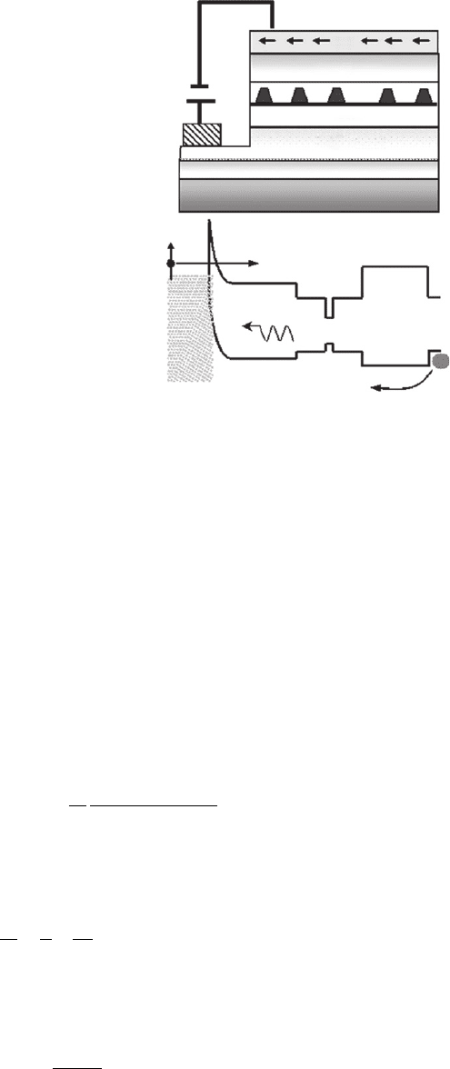
The device consists of an n-i-p light-emitting diode containing a QD active region back to back
with a Schottky diode formed by the Fe/ n –AlGaAs barrier, such that when the LED is in forward
bias then the Schottky diode is in reverse bias. Spin polarized electrons tunnel across the Schottky
barrier from the Fe contact and unpolarized holes are injected from the p -contact. Emission in the
growth direction is collected through the semi-transparent Fe contact. A schematic of the spin-
LED structure and a fl atband diagram of the device are shown in Fig. 3.33 .
The circular polarization, P
circ
, is analysed as a function of applied magnetic fi eld. Once effects
not related to spin injection (such as magneto-optical circular dichroism induced by the Fe contact
and Zeeman splitting of the QD exciton) are subtracted, a dependence of P
circ
on applied fi eld is
obtained, as shown in Fig. 3.34 , which can be fi tted by a Lorentzian function given by [271, 285] :
SS
T
T
T
z
S
S
S
init
τ
θθΩ
Ω
()
()
2
2
1
cos sin
where S
z
is the spin component in the growth direction, which is equal to P
circ
from the selection
rules, T
S
is the QD ground state exciton spin lifetime, defi ned by:
111
T
SS
ττ
where τ is the exciton radiative lifetime and τ
S
is the exciton spin relaxation time. The half-width
B
1/2
of the Lorentzian is given by:
B
gT
BS
12/
*
μ
Fe
n-AIGaAS
GaAs
QDs
p-AIGaAs
p-GaAs
p-GaAs substrate
(a)
(b)
InAs QDs
Figure 3.33 (a) Schematic of spin-LED structure, (b) fl atband diagram of the spin-LED. Reprinted with permis-
sion from Itskos et al. , Appl. Phys. Lett. 88 , 022113 (2006) [281] , Copyright 2006, American Institute of
Physics.
CH003-I046325.indd 118CH003-I046325.indd 118 6/25/2008 12:34:18 PM6/25/2008 12:34:18 PM