Henini M. Handbook of Self Assembled Semiconductor Nanostructures for Novel devices in Photonics and Electronics
Подождите немного. Документ загружается.

Growth and Characterization of ZnO Nano- and Microstuctures 309
2.0 2.2
Photon energy (eV)
2.4 2.6
2.8
Polarizer orientation:
PL intensity (arb. units)
Ec(TM)
0.3
N 5
N 6
N 7
P
0.2
0.1
0.0
2.0 2.2 2.4 2.6 2.8
(TE)Ec
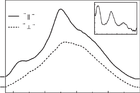
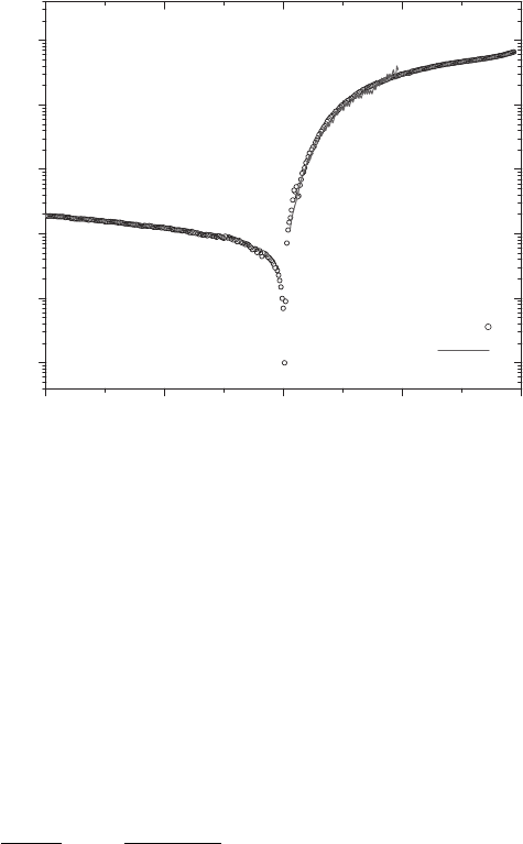
Figure 9.17 Micro-photoluminescence spectra of the nanoneedle of Fig. 9.15 for D ⬇ 790 nm at two different
polarizer azimuth orientations shifted vertically for clarity. The modulation of the VIS band almost disappears when
detecting the TE mode. Thus, the resonances are mainly TM polarized. The inset shows the ratio P ( I
TM
– I
TE
)/
( I
TM
I
TE
), which visualizes the TM-WGMs as distinguishable peaks. The polarization effect has been found to be
independent of the polarization of excitation.
suppression of WGM modulations (see Fig. 9.17 ). The remaining spectrally unstructured emis-
sion occurs due to the unpolarized character of ZnO photoluminescence originating from the
needle’s centre. However, this result is consistent with former investigations of lasing in hexago-
nal cavities within the micrometre regime that are reported to emit only TM modes [101] . Hence,
in comparison with TE modes, TM modes obviously exhibit lower losses. This can be generally
understood since, leaving the regime of TIR, the refl ection coeffi cient for TM polarized waves due
to Fresnel’s equations is always larger than that for TE polarized ones.
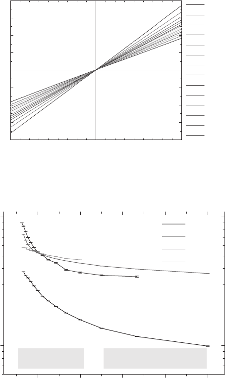
9.3.4.4 Theory vs experiment
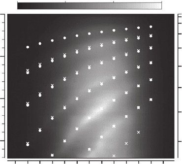
To compare the measured energies of the WGMs in nanostructures with theoretically predicted
ones for both types of polarization, a spectral line scan along the needle’s longitudinal axis
is given in Fig. 9.18 . In grey scales, the resonances appear as a set of bright lines that actually
exhibit a curvature as expected from Eq. 9.2. The theoretical values are shown with dots and
cross symbols in Fig. 9.18 . They are directly calculated without free parameter using the experi-
mentally determined shape of the needle, i.e. R
i
( x ), see Fig. 9.15 , and the above-mentioned thin
fi lm data for
nE
||
()
and n
⬜
( E ) [90] . The dots (TM) match the measured resonance energies with
a very good agreement. Additionally, the well fi tting blue arrows within Fig. 9.16a confi rm that
the simple PWM gives a good description of the basic physics of WGMs even in nano-sized crystal
geometries within the limits of the resonance linewidths.
9.3.4.5 Line broadening effects
As shown in Fig. 9.16 , compared to microcavities, nano-sized crystals show broadened WGMs
due to the increase of losses with decreasing cavity diameter. Nevertheless, CLI of the broad VIS
band still enables the visualization of WGMs in the ZnO nanoneedle even at diameters D λ / n 艑
270 nm.For mode numbers N 4 single TM-WGMs can be detected unambiguously as distin-
guishable maxima modulating the broad VIS band. For smaller mode numbers N 3 W G M s
can only be visualized as a continuous blue shift of the intrinsic VIS maximum, and the discon-
tinuities in Fig. 9.16c and d become smooth. This is due to the extreme line broadening of both
types of WGMs with decreasing cavity diameter. Theory [97] predicts line broadening by loss
processes due to boundary waves that are scattered out of the resonator and due to light paths
whose angle of incidence is slightly deviating from 60 °. A relation FWHM E
1
R
2
is obtained,
which explains the dramatic broadening of the measured resonances. For TM polarization and
CH009-I046325.indd 309CH009-I046325.indd 309 6/24/2008 3:05:22 PM6/24/2008 3:05:22 PM
310 Handbook of Self Assembled Semiconductor Nanostructures for Novel Devices in Photonics and Electronics
N 6 (spectrum 1 of Fig. 9.16a ) a FWHM of about 350 meV is predicted. Considering that the
underlying theory again is prepared for N 1, the obtained spectrum verifi es this value within
the limits of resolution. For resonance N 3 the theoretical FWHM is about 900 meV, which
exceeds even the intrinsic linewidth of the VIS band. This explains the diffi culty to obtain distinct
WGM peaks for N 3. Nevertheless, VIS emission is still affected when a WGM crosses the VIS
range, as Fig. 9.18 clearly shows intensity modulations at the respective line scan positions. We
note that losses due to surface roughness of the cavity faces could also lead to line broadening.
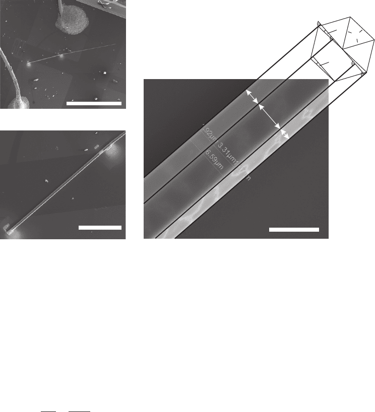
However, as the high resolution SEM image of Fig. 9.15c shows well-shaped resonator faces, we
do not adopt this loss process to be the dominating one.
9.3.4.6 Discussion
As mentioned above, there is an energy difference between predicted TM and TE modes. This dif-
ference is mostly due to β in Eq. 9.1, since the ZnO birefringence
() )nn nn
||||
/(
⊥⊥
⬇ 1.2% is
small [90] . However, TE mode with mode number N is predicted (coincidentally due to the partic-
ular value of n ) to appear very close to the spectral position of TM mode N 1 ( Fig. 9.18 ), and,
hence, this could be one reason for the missing TE mode series. Possible TE-WGM maxima should
always lie beyond higher-ordered TM maxima, and as the former ones suffer larger losses, they
lead to much broader resonance peaks hardly detectable in the VIS band.
Certainly there are, however, small deviations between the detected peak energies and the
predicted TM-WGMs according to Eq. 9.1. (see Figs 9.16a and 9.18 ). These deviations probably
reveal the limits of the simple PWM. To discuss this fact more in detail we note that the applica-
tion of numerical methods to predict resonance energies at the end always depends on a precise
determination of the considered geometry, e.g. R
i
, and a good knowledge of the refractive index n .
SE microscopy measurements of the cavity diameter D are performed with an error of at least 1%.
The ellipsometrically determined values for
n
||
for bulk material yield an error in n of about 2%.
The actual refractive index of the nanocrystals may possibly differ additionally. These effects lead
to an error in E of about 3%, i.e. 50–80 meV in the considered spectral range, which is indicated
800
600
Needle diameter (nm)
400
200
0
0
5
Scan position (m)
10
15
1.6 2.0
Photon energy (eV)
2.4 2.8
30 60 90
CL intensity (arb. units)
0
1
1
2
2
3
3
4
4
5
5
6
6
N
TM
N
TE
Figure 9.18 Two-dimensional plot of spectra recorded along a line scan on the needle’s longitudinal axis. The left
vertical axis shows the line scan position x, the right one refers to the respective needle diameter D. The grey scales
refer to the spectral CL intensity. The spectral maxima, i.e. the measured WGM energies, appear as bright belts going
from the bottom left corner to the right upper one. With decreasing diameter all resonances shift systematically to
higher energies. The white dots give theoretical TM resonance energy positions obtained from Eq. 9.1, white crosses
give the same for TE polarization. Without adjusting free parameters there is a very good agreement between experi-
ment and theory.
CH009-I046325.indd 310CH009-I046325.indd 310 6/24/2008 3:05:22 PM6/24/2008 3:05:22 PM

Growth and Characterization of ZnO Nano- and Microstuctures 311
as error bars in Fig. 9.16a . Compared to the linewidths of the WGMs, Eq. 9.1 for TM polarization
gives a very good description of the spectral position of the resonant modes.
9.4 Optical properties II: stimulated emission from ZnO microcrystals
In the last section we showed that micrometre-sized ZnO structures can be employed as optical
resonators are hence promising candidates for laser devices and should allow fundamental inves-
tigations of light–matter coupling. The microcrystal structures show a high photoluminescence
(PL) signal under low excitation conditions.
If ZnO is optically excited under high intensities, typically an additional peak arises in the ZnO
PL spectrum. This peak is most probably caused by an inelastic exciton–exciton scattering proc-
ess and exhibits a fi ne structure. The emitted photons have the energies [102] :
EE E
n
kT
nexx
b
B
1
13
2
2
⎛
⎝
⎜
⎜
⎜
⎞
⎠
⎟
⎟
⎟
⎟
(9.3)
where E
ex
is the energy of the free exciton luminescence, E
x
b
is the binding energy of the exci-
tons and k
B
T the thermal energy. The parameter n is the quantum number of the problem. The
respective peak is called P-band and in many cases stimulated emission related to this band can
be observed. Under even higher excitation, the carrier density in the sample increases and the
electron–hole plasma (EHP) peak at even lower energies than the P-band becomes observable.
A laser is a device emitting stimulated optical radiation. For practical purposes, one uses a cav-
ity for optical feedback. A ZnO microcrystal per se cannot be expected to act as such a cavity due
to the high losses caused by the short distance of the mirrors. The mirror loss for refl ectivities R
1
and R
2
in a cavity of length L is given by [103] :
α
21
12
LRR
ln .
(9.4)
The refl ectivity of the ZnO/air interface is approximately 0.2. For a 10 μ m cavity, Eq. 9.4 gives a
loss of 1600 cm
1
. In a real structure, other losses due to scattering and absorption will addition-
ally play a role. Typical gain reported for ZnO (150 cm
1
in [104] , 600 cm
1
in [105] ) cannot
overcome these losses. The observation of Fabry–Perot modes in lasing thus seems unlikely in
our structures. However, we will demonstrate stimulated emission as result of a single pass gain.
9.4.1 Experiments
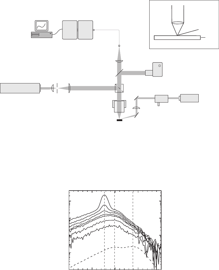
Figure 9.19 shows a scheme of the set-up used for the PL and high excitation spectroscopy (HES)
measurements. It allows spatially resolved PL measurements and the observation of emitted
light from single microstructures. For PL, the excitation source was a continuous-wave He–Cd
Kimmon laser with a wavelength of 325 nm and a power of 20 mW. For HES measurements, a
pulsed Thales DIVA II Nd:YAG laser beam (266 nm, 10 ns, 20 Hz) is focused on the sample. The
energy per pulse is 2 mJ. Using these two lasers, the excitation intensity has been varied in a
range from 1 to 2500 kW/cm
2
. The angle of incidence of the pump beam is approximately 60 °
with respect to the surface normal as depicted in the inset of Fig. 9.19 . Excitation spots smaller
than the diameter of the pump laser beam are possible using a focusing lens. Furthermore, the
excitation intensity can be controlled by a refl ective Newport attenuator for high power lasers.
The light emitted from the sample can be defl ected into a digital camera by a movable mirror
making the set-up work as an optical microscope. If the mirror is removed, the emitted light is
focused onto an optical fused silica fi bre and directed to the monochromator. It is then spectrally
dispersed with a 2400 lines/mm grating (blaze 330 nm) and detected by a liquid nitrogen cooled
back-illuminated CCD camera. The set-up is diffraction limited and confocal and allows a spatial
resolution of 1 μ m.
CH009-I046325.indd 311CH009-I046325.indd 311 6/24/2008 3:05:23 PM6/24/2008 3:05:23 PM
312 Handbook of Self Assembled Semiconductor Nanostructures for Novel Devices in Photonics and Electronics
9.4.2 Results and discussion
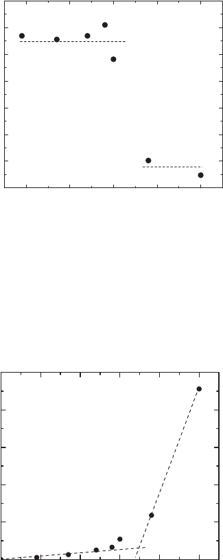
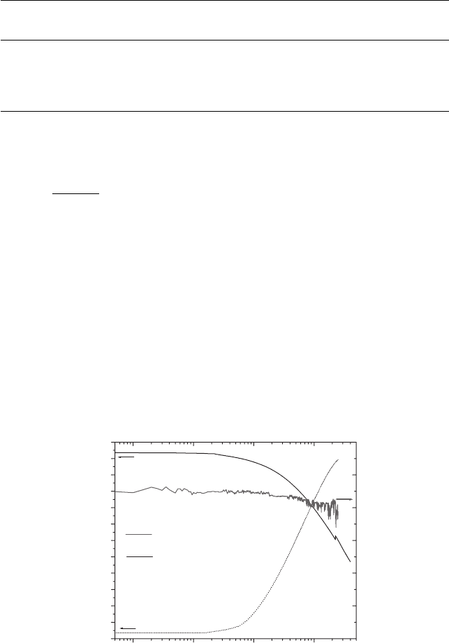
Figure 9.20 shows the low and high excitation spectra of a ZnO microcrystal in a semilogarithmic
plot at room temperature. The dashed cw spectrum was shifted for clarity and does not fi t to the
same scale. The excitation intensities were chosen between 45 and 250 kW/cm
2
.
He-Cd-Laser
Nd: YAG
Laser
Mono-
chromator
CCD
Pinhole
Beam splitter
Piezo
objective
Sample
Digital camera
Moveable mirror
Fibre
Computer
Attenuator
Nd: YAG
Laser
Objective
Crystal
c-axis
Figure 9.19 Set-up for spatially resolved PL measurements. The inset shows the orientation of the wire with
respect to the laser beam and the objective.
3.0 3.1
cw
45 kW/cm
2
250 kW/cm
2
PXX-LO
10
4
10
3
10
2
10
1
10
0
Intensity (arb. units)
3.2
Energy (eV)
3.3 3.4
Figure 9.20 Room temperature PL spectra of a ZnO microcrystal arranged on a carbon gluepad under low (dashed
curve) and high (solid curves) excitation intensities varied between 45 and 250 kW/cm
2
. At higher excitation inten-
sities, the P-band arises from the free exciton emission band. The dashed curve of the cw spectrum was shifted for
clarity.
Two peaks at 3.20 and 3.28 eV are observed in the cw spectrum. The lower energy peak is most
probably related to the fi rst LO-phonon replica of the 3.28 eV maximum. Under higher excitation
only the 3.20 eV peak is visible. It can be seen from Fig. 9.20 that a sharp peak at 3.154 eV is pre-
dominant in the spectrum for higher excitation intensities. The FWHM is 88 meV for 85 kW/cm
2
and 29 meV for 250 kW/cm
2
, indicating spectral narrowing as depicted in Fig. 9.21 .
CH009-I046325.indd 312CH009-I046325.indd 312 6/24/2008 3:05:23 PM6/24/2008 3:05:23 PM
Growth and Characterization of ZnO Nano- and Microstuctures 313
The peak intensity increases superlinearly with increasing excitation intensity as depicted in
Fig. 9.22 . The spectral narrowing ( Fig. 9.21 ) and the superlinear characteristic curve in Fig.
9.22 implies the presence of stimulated emission from the microcrystal. The threshold pump
intensity is approximately 170 kW/cm
2
.
Excitation density (kW/cm
2
)
50
20
40
60
80
100
120
FWHM (meV)
140
160
100 150 200 250
Figure 9.21 FWHM of the PL peak as a function of the excitation intensity. Dashed lines are guides to the eye.
Excitation density (kW/cm
2
)
500 100
E 3.154 eV
25
20
15
10
Intensity (arb. units)
5
0
150 200 250
Figure 9.22 Dependence of the peak intensity on the excitation intensity. The superlinear dependency is clearly
visible. The treshold intensity for the stimulated emission is approximately 170 kW/cm
2
.
For T 300 K, Eq. 9.3 gives values between 3.234 ( n 2) and 3.219 eV ( n ). The observed
values are smaller than those expected from Eq. 9.3. We tentatively attribute the laser peak to the
P-band and the energy shift of about 70 meV from the expected room temperature position to a
local increase of the sample temperature by approximately 100 K, taking into account the tem-
perature dependence of the band gap energy [106] . Further excitation density and temperature
dependence measurements will clarify this point.
9.5 Electrical characterization of ZnO microcrystals
Nanowires and nanotubes carry charge effi ciently and are potentially ideal building blocks for
future (opto)electronics. Knowledge about contacts and electrical conduction properties of
CH009-I046325.indd 313CH009-I046325.indd 313 6/24/2008 3:05:24 PM6/24/2008 3:05:24 PM
314 Handbook of Self Assembled Semiconductor Nanostructures for Novel Devices in Photonics and Electronics
ZnO is essential for practical device applications. In 1965, Mead [107] investigated surface bar-
rier heights of several metals on vacuum cleaved ZnO surfaces. For thin fi lms and bulk material
there are several recent reports on electrical characterization of ZnO, e.g. by H. von Wenckstern
et al. [108] or D.C. Look et al. [16] . However, for single nano- and microsized ZnO crystals there
are only a few experimental results on electrical transport and contacts, e.g. [109, 110] . For
instance, Park et al. investigated the electrical transport mechanism of single ZnO nanorods
[111] . Also some prototype devices have been demonstrated including fi eld effect transistors
(FET), p–n junctions and electroluminescent nanodevices (grown on p-GaN) on the basis of ZnO
nanostructures [41, 112] . The large surface-to-volume ratio of such structures is expected to
cause a strong dependence of the transport properties on environmental conditions, a fact that
makes ZnO nanowires ideal candidates for sensing applications [43, 44] .
In this section the results of rectifying and ohmic contacts on ZnO microwires will be presented
and the temperature dependence of the conductivity will be discussed.
1.0 0.5
0.0
Voltage (V)
0.5
Experiment
fit
Fit parameters
Reverse current 1.235 pA
Ideality factor 1.42
Series resistance 989 M?
Barrier height 0.717 eV
1E9
1E10
Current (A)
1E11
1E12
1E13
1E14
1.0
Figure 9.23 Current vs voltage characteristic of a ZnO microwire with an Epo-Tek H20E rectifying contact. The
parameters of the fi t according to Eq. 9.5 (red curve) are shown in the inset.
The dependence of the current I on the applied bias of a carbothermally grown microwire with
one rectifying contact (Epo-Tek H20E) and one ohmic contact (GaIn) was measured at room temper-
ature with the semiconductor parameter analyser and a wafer prober. A typical rectifying diode-like
behaviour with a forward/reverse current ratio around 350 is observed. According to the Schottky–
Mott model, the barrier formation can be described by the barrier height which is given by the dif-
ference of the Fermi level of the contact metal and the electron affi nity of the semiconductor [113] .
Reports on investigations in the temperature range between 300 and 500 K from several groups
reveal a transport mechanism according to the thermionic emission model [43, 110] . In order
to determine the diode key fi gures, the forward current was fi tted under the standard assumption
that thermionic emission is the dominating current transport process at room temperature [114] :
IAAT
kT
eV IR
nk T
B,eff
as
B
*
exp exp
2
Φ
⎛
⎝
⎜
⎜
⎜
⎜
⎞
⎠
⎟
⎟
⎟
⎟
⎛
⎝
⎜
⎜
⎜
⎜
⎞
⎠
⎟
⎟
⎟
()
⎟⎟
⎡
⎣
⎢
⎢
⎢
⎤
⎦
⎥
⎥
⎥
1
(9.5)
where A is the contact area, A
*
is the effective Richardson constant having a theoretical value
of 32 Acm
2
K
2
(for m
e
*
0 . 2 7 m
0
[103, 114] , T is the absolute temperature, Φ
B
,
eff
is the effec-
tive barrier height at zero bias, e is the elementary charge, V
a
is the applied voltage, R
S
is the
CH009-I046325.indd 314CH009-I046325.indd 314 6/24/2008 3:05:24 PM6/24/2008 3:05:24 PM
Growth and Characterization of ZnO Nano- and Microstuctures 315
series resistance, n is the ideality factor of the diode and k
B
is Boltzmann’s constant. The effective
Schottky barrier height was determined to be Φ
B
,
eff
0.72 eV and the ideality factor was 1.42.
For ZnO thin fi lms and single crystals similar values have been reported for Ag as a Schottky con-
tact metal: a barrier height of 0.56–0.84 eV [115, 116] and ideality factors between 1.33 and
1.5 were obtained from I – V and C – V (capacitance–voltage) measurements [115, 117] .
0.05
4
3
2
1
0
1
2
3
0.00
Volta
g
e (V)
0.05
Wire2
Current (µ A)
OhmicW contacts
(deposited by FIB)
40
T(K)
60
80
100
120
140
160
180
200
220
240
260
280
300
Figure 9.24 Temperature-dependent current–voltage characteristics of wire 2. It shows an ohmic behaviour due to
the two tungsten contacts which were attached to the microwire with the FIB.
G (S)
100/T(K
1
)
510 2015 25
Impurity band or conductive
surface channel
Wire 1
Wire 2
Wire 3
Wire 4
Thermal activation
of donors
10
100
Figure 9.25 Temperature dependence of the conductivity of four different ZnO microwires. At low temperature the
conduction is very weakly temperature dependent and apparently governed by a surface channel or an impurity band
(see text).
The temperature dependence of ohmic I – V characteristics has been measured for four different
microwires in the dark in a closed cycle helium cryostat with a semiconductor parameter ana-
lyser (Agilent 4156C). Wires 1 and 2 were prepared with two FIB-deposited tungsten contacts
and wires 3 and 4 with two InGa contacts each. Figure 9.24 shows the result of the tempera-
ture range from 40 up to 300 K for wire number 2. As expected, it shows an ohmic behaviour
CH009-I046325.indd 315CH009-I046325.indd 315 6/24/2008 3:05:25 PM6/24/2008 3:05:25 PM
316 Handbook of Self Assembled Semiconductor Nanostructures for Novel Devices in Photonics and Electronics
and the resistance (inverse slope) decreases with increasing temperature. The other three crys-
tals showed qualitatively exactly the same response. This dependence was analysed in more detail
by linear fi tting of the I – V curves. Figure 9.25 shows the Arrhenius plot of the corresponding
conductivities G 1 / R . The very small vertical bars in the plot indicate the error obtained from
the linear fi tting of the slope of the I – V curves. In the temperature regime from 200 to 300 K
all samples show a strongly temperature dependent conduction. At low temperatures, i.e. in the
freeze-out range, the conductivity is almost temperature independent, which is especially pro-
nounced for wires 2 and 4. This can be attributed either to a conductive surface channel or to
an impurity band conduction process. In order to provide the fundamentals for nanowire device
applications, it is essential to study the crucial electrical parameters, like, for example, the carrier
concentration (defi ned by the doping level) and carrier mobility. However, to do so independently,
experiments such as temperature-dependent Hall measurements need to be performed which are
connected with obvious diffi culties for micro- and nanosized structures. But also from the present
data the carrier concentration can be estimated.
100 µm
500 µm
(a)
(b)
a
b
c
R
5 m
(c)
Figure 9.26 (a), (b) SEM pictures of a carbothermally grown ZnO microwire with two tungsten contacts at differ-
ent magnifi cations. (c) illustrates the geometrical considerations for the determination of R which account for the tilt
of the crystal.
The specifi c conductivity for electron and hole conduction can be written as [103] :
σμμ en ep
np
(9.6)
where e is the electron charge, n and p are the electron and hole densities, respectively, and μ
i
is the corresponding charge carrier mobility. Since ZnO is intrinsically n -conducting [118] , the
p -conducting part is negligible here and the electron density can be estimated by:
n
e
lG
Ae
nn
≈
σ
μμ
(9.7)
CH009-I046325.indd 316CH009-I046325.indd 316 6/24/2008 3:05:25 PM6/24/2008 3:05:25 PM

Growth and Characterization of ZnO Nano- and Microstuctures 317
where l is the length and A is the area of the hexagonal cross-section. It is given by:
AR
33
2
2
(9.8)
where R is the radius of the circumscribing circle as indicated in Fig. 9.26 . The length, as well as
the projected distances between the edges of the hexagons:
aR
bR
cR
cos
cos
sin
()
()
60
30
α
α
α
(9.9)
of the ZnO microwires, can be determined from top-view SEM pictures (see Fig. 9.26 ). Each pair
of those equations can be solved for the tilt angle α by eliminating R :
α
α
α
arctan
arctan
()
arctan
2
32
3
3
3
3
3
()
()
()
ab
b
ac
ab
bc
b
(9.10)
Once α is known, R can be calculated:
abc R R
abc
2
2
cos
cos
α
α
⇔
(9.11)
The mobility of ZnO above 200 K is limited mainly by polar optical phonon scattering [103] .
Since the crystal structure of the ZnO micro- and nanowhiskers investigated here is very good,
the mobility is not limited by grain boundary scattering, as is usually the case for PLD-grown
ZnO thin fi lms [108] . Hence, the temperature dependence of the Hall mobility of commercially
available single ZnO bulk crystals grown by seeded chemical vapour deposition (Eagle Picher Inc.)
can be taken as a good appoximation for the microwires in the temperature regime above 200 K.
The values from sample A in [108] have been used to determine the carrier density according to
34 56
29
30
31
Wire 1
Wire 2
Wire 3
Wire 4
Linear fit
ln(n/T
3/2
) (arb. units)
1000/ T(K
1
)
Figure 9.27 Temperature dependence of the carrier concentration of ZnO microwires. The carrier activation energy
for 240–300 K can be extracted from the slope (cf. Eq. 9.12).
CH009-I046325.indd 317CH009-I046325.indd 317 6/24/2008 3:05:26 PM6/24/2008 3:05:26 PM
318 Handbook of Self Assembled Semiconductor Nanostructures for Novel Devices in Photonics and Electronics
Eq. 9.7. It should be noted that a considerably lower room temperature mobility (17 cm
2
/Vs) was
estimated from the transconductance of nanowire FETs [43] . The room temperature results are
summarized in Table 9.2 . The carrier concentration varies between 1.22 1 0
16
cm
3
(wire 2)
and 1.94 1 0
17
cm
3
(wire 4).
Table 9.2 Tilt angle, length and radius, as well as room temperature conduc-
tivity, the estimated carrier concentration and the thermal carrier activation
energy of the four microcrystal samples
Wire
α (°)
l ( μ m) R ( μ m)
G (300 K) (S)
n (300 K) (cm
3
)
Δ E
(meV)
1 5.49 234.06 3.31 3.77 1 0
5
9.58 1 0
16
30.09
2 0.22 138.60 7.13 7.34 1 0
5
1.22 1 0
16
37.60
3 12.79 330.83 9.4 2 5.80 1 0
5
2.57 1 0
16
18.41
4 1.47 2240.00 10.80 8.51 1 0
5
1.94 1 0
17
39.59
The temperature dependence of the electron concentration in the Boltzmann approximation
can be written as [103] :
nN
EE
kT
C
FC
B
exp
(9.12)
where E
F
is the Fermi energy, E
C
is the conduction band energy and N
C
is the conduction band
edge density of states which is proportional to T
3/2
. Hence, the thermal activation energy E
F
E
C
can be determined from the slope in a ln( n / T
3/2
) vs 1/ T plot. The results are shown in Fig. 9.27
with n determined by Eq. 9.7 using again the temperature dependent mobility from [108] . The
activation energies were determined from the linear fi t of the range from 240 to 300 K and are
summarized in Table 9.2 . The values are between 18 and 40 meV. It was reported for undoped
ZnO that native defects of zinc interstitials contribute to the n -type semiconducting behaviour,
and these defects serve as shallow donors with a binding energy of 30–60 meV [16] . Other stud-
ies based on PL spectroscopy, temperature-dependent Hall experiments or electrical conductiv-
ity measurements report on typical activation energies between 11 and 53 meV for nominally
undoped ZnO [119–121] . Hence, the microwires seem to have similar contact properties and the
conduction mechanism is, apart from surface effects, comparable to bulk ZnO.
Current (µA)
Current (µ
A)
Light on
Light off
0.60
0.55
0.50
0.45
0.40
0.35
0.30
0.25
0.20
0.15
0.10
0.05
0.00
Nanowire
PLD thin film
Time (s)
1 100 1000
6
5
4
3
2
1
0
Figure 9.28 Time dependence of the current through a nanowire. As a comparison the persistent photocurrent of a
PLD thin fi lm is shown (black solid line) as well as the photoresponse (black dotted line).
CH009-I046325.indd 318CH009-I046325.indd 318 6/24/2008 3:05:27 PM6/24/2008 3:05:27 PM