Henini M. Handbook of Self Assembled Semiconductor Nanostructures for Novel devices in Photonics and Electronics
Подождите немного. Документ загружается.

Miniband-related 1.4–1.8 μ m Luminescence of Ge/Si Quantum Dot Superlattices 329
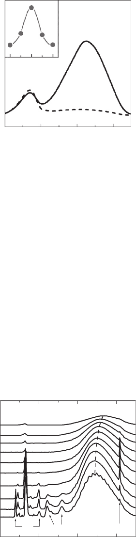
PL spectrum the QDSL band is very weak. Sb doping leads to the noticeable improvement of PL
properties in the spectral range (1.4–1.8) μ m – QDSL band becomes dominant. The maximum
effect is observed for 20 s exposition (the inset in Fig. 10.5 ). At higher Sb doses the QDSL PL is
quenched again. All results presented below are produced on the Ge/Si QDSLs doped with a 20 s
Sb exposition.
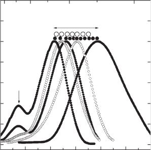
The PL spectrum of Ge/Si QDSL for different measurement temperatures between 5 and 80 K
is shown in Fig. 10.6 . The high-energy part of the low-temperature PL spectrum contains a
group of narrow lines related to the carrier radiative recombination in the Si matrix. Basically, it
is the band–band recombination assisted by the TA, TO and (TO O
Γ
) phonons, and the lines of
bound excitons. The fundamental Si
TO
line is detected in the PL spectrum up to room temperature
( Fig. 10.5 ). At temperatures below 20 K two bands marked as WL
NP
and WL
TO
are observed in
the middle part of the PL spectrum. Most authors explain these bands by the carrier recombi-
nation in the Ge WL: non-phonon and TO–phonon assisted, respectively. It should be noted that
dislocation PL lines D3 and D4 could be found in the same spectral region [24, 25] . In our case,
however, the WL
NP
and WL
TO
bands cannot be associated with a D3 and D4 dislocation PL. We
have not observed D3 and D4 lines even for specially dislocated structures [26] . Besides, the spec-
tral positions of WL
NP
and WL
TO
bands change depending on the WL thickness, namely in a
structure with a thicker Ge layer both WL bands are shifted in the low-energy direction.
QDSL
Sb doped
Sb exposition (s)
Si
TO
Undoped
1200
02040
1400
Wavelength (nm)
PL intensity (a.u.)
1600
Figure 10.5 Room temperature PL spectra of two QDSLs: undoped and Sb doped with 20 s exposition. The
inset shows the infl uence of Sb exposition time on the PL intensity of the QDSL band. Excitation power density
P 6 Wcm
2
. The QDSLs are grown on a p -type substrate.
Si
C-O
Si WL
NP
TO
Si
TO
QDSL
1200 1400
Wavelength (nm)
PL intensity (a.u.)
1600
Figure 10.6 PL spectra of QDSL at different measurement temperatures: 5, 10, 15, 20, 25, 30, 40, 50, 60,
80 K, from the bottom to the top. P 6 Wcm
2
. The QDSL is grown on p -type substrate.
CH010-I046325.indd 329CH010-I046325.indd 329 6/27/2008 4:28:46 PM6/27/2008 4:28:46 PM
330 Handbook of Self Assembled Semiconductor Nanostructures for Novel Devices in Photonics and Electronics
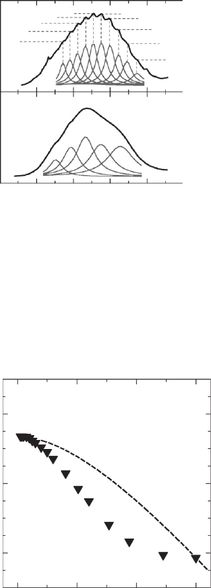
The broad QDSL band in the low-energy part of the PL spectrum is attributed to the optical
transitions in the Ge/Si columns between holes, localized in the QDs, and electrons, tied to the
interface by Coulomb interaction [8–10, 27–32] . At temperatures T 10 K the fi ne periodic
structure of the QDSL band is distinctly observed. The deconvolution into 10 Lorentzians is
the best fi t of the observed multi-modal structure [ 5 ; 5] ( Fig. 10.7a ). The average distance
between neighbouring maxima is δ
m
10 meV. The full width at half maximum of the compo-
nent is FWHM 15 meV. The QDSL embedded into a p
– n
-junction has the structure of the
QDSL PL band too ( Fig. 10.7b ), but the number of components is only 5 [ 3 ; 2], the distance
δ
m
is larger (about 20 meV) and the FWHM is 30 meV. On the other hand, this multi-modal struc-
ture was kept in the PL spectrum of an LED up to 150 K.
5
3
2
1
1
2
(a)
(b)
0.75 0.80
Photon energy (eV)
PL intensity (a.u.)
0.85 0.90
4
3
2
1 1
2
3
4
5
Figure 10.7 QDSL PL band measured at 5 K and an excitation density of 6 Wcm
2
for two Ge/Si QD structures:
(a) grown on p -type substrate (see Fig. 10.6) and (b) on p
-type substrate. Deconvolution into Lorentzians is also given.
0.84
0.80
0.76
0 100 200
300
PL peak energy, E
m
(eV)
Temperature (K)
QDSL
E
GeSi
(T)
Figure 10.8 Temperature dependence of the QDSL PL peak energy E
m
. Excitation power density amounts to
6 Wcm
2
. The dashed line shows the temperature dependence of the bulk Ge
0.8
Si
0.2
band gap. Composition x 0.8
is equivalent to the Ge content in QDs. The QDSL is grown on p
-type substrate.
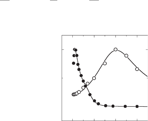
The temperature dependence of the QDSL PL peak energy ( E
m
) for a p
–( i )– n
-structure
is more informative and is shown in detail in Fig. 10.8. A pronounced red shift of E
m
occurs at
lower temperatures than the corresponding band gap narrowing of bulk GeSi. The deviation
starts as early as 20 K, reaches a maximum in the range 150–200 K and disappears at 300 K.
The pronounced red shift of the PL peak is typical for In(Ga)As/GaAs QDs, but not earlier than
at 100 K. It has been attributed to carrier redistribution between small and large QDs [33–35] .
CH010-I046325.indd 330CH010-I046325.indd 330 6/27/2008 4:28:47 PM6/27/2008 4:28:47 PM
Miniband-related 1.4–1.8 μ m Luminescence of Ge/Si Quantum Dot Superlattices 331
0 100 200 300
1
0
J/J
0
(a.u.)
E
A
65 meV
E
A
55 meV
Temperature (K)
Figure 10.9 Temperature dependence of the QDSL PL integrated intensity for two structures. Filled circles – QDSL
on the p -type substrate. Open circles – QDSL on the p
-type substrate. PL excitation density – 6 Wcm
2
. Solid lines –
fi t using Eq. 10.1. Activation energies E
A
deduced from the fi t are also shown.
In our system, the early red shift is caused by other mechanisms which will be discussed on the
basis of an energy band model below.
The temperature dependence of the QDSL integrated intensity ( J ) is presented in Fig. 10.9 for
both types of structures. For an analysis, an energy E
A
for thermal-activated electrons leaving
the states contributing to PL is introduced. The activation energy E
A
was calculated from an
Arrhenius plot. We used extended Arrhenius analysis. Beside the main quenching mechanism
of PL with E
A
we took into account an additional competing transition with E
A
2
. Experimental
points were fi tted using the following expression:
JT
J
A
E
kT
A
E
kT
AA
()
()
exp exp
0
1
12
2
⎛
⎝
⎜
⎜
⎜
⎞
⎠
⎟
⎟
⎟
⎟
⎛
⎝
⎜
⎜
⎜
⎞
⎠
⎟
⎟
⎟
⎟
⎡
⎣
⎢
⎢⎢
⎤
⎦
⎥
⎥
1
(10.1)
where J (0) is maximal PL intensity, A
1
, A
2
are fi tting parameters and k is the Boltzmann’s con-
stant. The values of the main activation energy E
A
for the two samples are shown in Fig. 10.9 .
The Arrhenius analysis was applied to obtain the activation energy for a set of structures hav-
ing different values of the QD height B and the spacer thickness W . Fig. 10.10 shows that the
activation energy in QDSLs does not depend on the QD size B ( Fig. 10.10c ), but on the spacer
thickness W ( Fig. 10.10d ). This means that the Si spacer in the column acts as a real QW with a
discrete level for electrons ( Fig. 10.11 ). In fact, the main activation energy E
A
is the barrier height
for electrons on this level, and it is determined as the difference between the QW depth (conduc-
tion band offset U
e
) and confi nement energy of electron ground state E
e
. As W increases (3.0–
6.6 nm), the electron 1 e level goes down, and main activation energy increases (45–85 meV).
The competing activation energy E
A
2
has been kept between 6 and 10 meV. If parameter A
2
is
positive, the second term is responsible for the early but slow temperature quenching of the QDSL
PL, for example at relatively low excitation of QDSLs embedded into a p–n -junction. In case of
a negative parameter A
2
the second term in (10.1) is responsible for the temperature-induced
enhancement of the QDSL PL, for example at relatively low excitation of QDSLs embedded into
a p
– n
-junction. The PL intensity increase in a certain temperature interval is typical for the
majority of QDSLs. Figure 10.9 shows how the QDSL band intensity grows in the range 5–20 K
for the p– (QDSL)– n -structure and in the range 5–200 K for the p
–(QDSL)– n
-structure.
The upper part of Fig. 10.10 presents the QDSL peak position E
m
as a function of QD height B
and spacer thickness W for a set of structures investigated. It should be noted that E
m
in the PL
spectrum obviously does not depend on the Si spacer thickness W in the column ( Fig. 10.10b ),
CH010-I046325.indd 331CH010-I046325.indd 331 6/27/2008 4:28:48 PM6/27/2008 4:28:48 PM
332 Handbook of Self Assembled Semiconductor Nanostructures for Novel Devices in Photonics and Electronics
but on the Ge QD height B ( Fig. 10.10a ). Specifi cally, as B increases, the QDSL band has a lower
energy position. This phenomenon is in full agreement with the assumption that in the Ge/Si
heterostructures the radiative recombination energy of the electron–hole pair mostly depends on
the heavy-hole level in the deep QW of the Ge layer [36] . As the Ge QD size increases, the hole
confi nement energy E
hh
decreases, which results in a lower transition energy E
m
.
The energy band line-up shown in Fig. 10.11 can be considered as the initial approximation
for the studied Ge/Si QDSLs. Potential wells are formed for the holes in the Ge QDs as well as for
the electrons in the Si spacer layers. The Ge QW for holes is characterized by a depth of up to
several hundreds of meV and, thus, the thermal redistribution of holes is negligible for the Ge/Si
880
840
800
760
80
60
40
880
840
800
760
80
60
40
E
m
(meV)
E
m
(meV)E
A
(meV)
E
A
(meV)
345 3456
B (nm) W (nm)
345 3456
B (nm) W (nm)
(a) (b)
(c)
(d)
Figure 10.10 QDSL peak position in the low-temperature PL spectrum ( E
m
) and the main activation energy ( E
A
)
of the QDSLs as a function of QD height B and spacer thickness W . The values of B and W are measured on the
column axis using TEM data. The PL excitation power density is 6 Wcm
2
. The solid lines are given for clarity.
Ge
Ge
Si
1e
1hh
z
U
h
E
Si
E
Ge
E
m
U
e
E
e
E
A
E
hh
E
Ah
Figure 10.11 Scheme of type-II heterostructure with QWs for holes in the Ge layer and for electrons in the Si
layer. U – band offset, E
e
– confi nement energy of electron ground state, E
A
( U
e
E
e
) – activation energy of this
state, E
m
– optical transition energy (QDSL peak position). E
Ge
and E
Si
– band gaps of bulk Ge (QD) and Si (spacer)
for Δ valley with intermixing.
CH010-I046325.indd 332CH010-I046325.indd 332 6/27/2008 4:28:48 PM6/27/2008 4:28:48 PM
Miniband-related 1.4–1.8 μ m Luminescence of Ge/Si Quantum Dot Superlattices 333
structures. It is evident that the rapid red shift of the QDSL peak with temperature ( Fig. 10.8 ) is
explained by the processes in the electron subsystem. The localization of electrons in the Ge/Si
interface is mainly determined by the Coulomb interaction, i.e. by the indirect exciton binding
energy, which is constant and equals 25 meV [36] . The latter value is close to kT at room tem-
perature, making an observation of the QDSL band at room temperature quite diffi cult [8–14] .
In our highly strained Sb-doped QDSLs the potential well for electrons is deeper due to the ten-
sile strain–induced lowering of the conduction band. This leads to higher activation energies for
electrons (45–85 meV). This fact, however, cannot be the reason for the observed red shift of the
QDSL PL peak either.
Available experimental data on the activation energy for the QD PL band in Ge/Si structures
are very controversial and scattered between 15 and 183 meV [9, 10, 13, 37] . It is noteworthy
that only values between 21 and 46 meV are attributed to the electron subsystem in [13] . All
other reported values are interpreted as the hole escaping from the Ge QDs into the WL or barrier
lowered by intermixing. Close to 1.55 μ m the well-known D1 PL line can also be found, and this
line is attributed to dislocations in Si and has an activation energy of 170 meV [38, 39] . It should
be noted that our QDSL-related PL band has nothing in common with the D1 line (except the
spectral position) [40] . The QDSL PL peak position could be controlled by choosing the growth
parameters, which can change the Ge QD sizes. Figure 10.12 presents the PL and the EL spec-
tra of the Ge/Si QDSLs, which were produced by combining different parameters. The QDSL
PL peak dominates at room temperature. Its integrated intensity exceeds the Si
TO
fundamental
emission by a factor of 10 to 1000. The experimentally obtained positions of the QDSL maxima
are denoted by circles. They correspond to the spectral region of 1.4 μ m (0.89 eV) to 1.8 μ m
(0.69 eV).
1.2 1
0.8 0.6
1400 1800
Wavelength (nm)
Normalized PL intensity (a.u.)
QDSL
Si
TO
Photon energy (eV)
Figure 10.12 PL and EL spectra of Ge/Si QDSLs at room temperature. Full circles – PL, empty circles – EL. Circles
on the top denote the QDSL peak positions reached in the experiments.
The LED structures have a p
-type substrate and an Sb concentration profi le shown in Fig.
10.1c . In fact, during the carrier injection the Ge/Si QDSL having 20 periods acts as the active
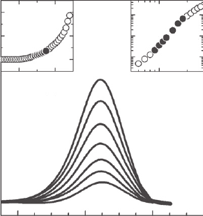
zone. The EL spectra for different current densities at room temperature (300 K) are presented in
Fig. 10.13 . The current–voltage characteristics of LEDs (the left inset of Fig. 10.13 ) demonstrates
the high-quality p
– n
-junction with a low dark current. At an increase of the current density
( j ) the integrated EL intensity ( J ) grows superlinearly. The right inset of Fig. 10.13 presents this
dependence ( J j
m
) in a double logarithmic plot. In the range of current densities j (0.9–1.8)
Acm
2
a factor m 4.8 is derived, at which the EL spectra in Fig. 10.13 are measured. For opti-
cal pumping the value of m -factor does not exceed 1.65 at room temperature [41, 42] . We have
CH010-I046325.indd 333CH010-I046325.indd 333 6/27/2008 4:28:48 PM6/27/2008 4:28:48 PM
334 Handbook of Self Assembled Semiconductor Nanostructures for Novel Devices in Photonics and Electronics
reported [43] such an unusually large m -factor for Ge/Si QDSL EL. It has the same nature as the
anomalous temperature dependence in Figs 10.8 and 10.9 and will be discussed below after con-
sideration of the energy band model of QDSL. Concerning all available publications, only in [14]
the J ( j ) dependence in Ge/Si QD multilayer structures at 300 K was measured. At j 20 Acm
2
the dependence was also found to be superlinear with a factor of 1.3. The authors of [11] meas-
ured the EL signal from a Ge/Si QD array up to 290 K. It is noteworthy that the QDSL EL intensity
was maximal at 225 K.
Our result ( m 4.8) demonstrates a high effi ciency for an electrical pumping of Ge/Si QDSLs
[43] . The external QE of the EL was measured for the QDSL band with a maximum at 1.55 μ m.
At a current density of 2 Acm
2
, the external effi ciency was η 4 1 0
4
. To the knowledge
of the authors this achieved value is the highest for Ge/Si structures in this spectral region at
ambient temperature. This value is higher than the external effi ciency reported for the QD-based
Ge/Si LEDs ( η 1 0
6
for λ 1 . 4 μ m, [44] ). In [12] , the same authors report the following val-
ues of internal QE in the Ge QD-based structures: 10
5
for the 10 layer structure and 5 1 0
6
( λ 1 . 4 2 μ m) for the one layer QD array. Normally, the effi ciency of LEDs based on band-to-band
luminescence in bulk silicon ( λ 1 . 1 2 μ m) is 10
4
–10
5
[45] . The LEDs based on dislocation-
rich silicon are characterized by an external QE of 10
6
( λ 1 . 6 μ m) [46] . Only a special surface
treatment of the highly purifi ed silicon wafer is allowed to reach η (1 – 2) 1 0
3
for the dislo-
cation luminescence [47] .
10.3.3 Effect of Sb doping
The unusually high localization potential for electrons in QDSLs (up to 85 meV) is related to the
extremely strained Ge/Si columns. It is known [48] that Sb is a perfect surfactant for the growth
of the Ge/Si heterostructures. The Sb predeposition leads to a decrease of the Si adatom migra-
tion. In this way antimony blocks possible channels of elastic strain relaxation in the Si spacer
layers, namely it suppresses intermixing and prevents the nucleation of dislocations. The accu-
mulation of tensile strain in the Si layers and a compressive strain in the Ge QDs leads to an
increase of U
e
, i.e. to the deepening of the electron QW. Values of the activation energy become
2–3 times larger than the thermal energy at room temperature ( kT 25 meV) and account for its
dependence on thickness W of the Si spacer ( Fig. 10.10 ). In [49, 50] it was possible to get room
I
0.1
0
10
1200 1600 2000
0.5 1 2
0.0
(A)
10
1
10
0
JJ j
m
m 4.8
QDSL
EL intensity (a.u.)
Bias (V) j (A/cm
2
)
Wavelength
Figure 10.13 Ge/Si EL spectra measured at room temperature for QDSL, having B 3.8 nm, W 2 . 5 n m .
Current densities j (Acm
2
): 0.9; 1.0; 1.1; 1.2; 1.4; 1.6 and 1.8, from the bottom to the top. Left inset: Dark
current–voltage characteristics. Right inset : Double logarithmic plot for EL integrated intensity J versus current
density j . Factor m is deduced from fi t J j
m
. Full circles correspond to the EL measurement points shown in the
main graph.
CH010-I046325.indd 334CH010-I046325.indd 334 6/27/2008 4:28:49 PM6/27/2008 4:28:49 PM
Miniband-related 1.4–1.8 μ m Luminescence of Ge/Si Quantum Dot Superlattices 335
temperature luminescence from Ge/Si strained layer superlattices probably due to the Sb predepo-
sition during the MBE growth. In [51] the post-growth Sb modulation doping of the Ge/Si super-
lattice resulted in an electron mobility enhancement at room temperature. Electron localization
with a band offset of U
e
100 meV was also reported in [9] for undoped Ge/Si nanostructures.
Our undoped Ge/Si multilayer structures have less sharp interfaces ( Fig. 10.1a in compari-
son to Fig. 10.1b ) and are characterized by a poor near-infrared PL ( Fig. 10.5 ). The same result
was produced by a number of special methods directed towards the improvement of intermixing
(smearing of interfaces): an increase of the growth temperature, a decrease of the growth rate
[26] and a post-growth annealing [52] .
Below we will provide a qualitative analysis of the Si QW profi le in Sb-doped QDSLs. It is evi-
dent that due to the well-defi ned interfaces the QW energy walls are practically vertical. The
QW energy bottom is likely to be non-symmetrical, because the tensile strain in the Si spacer is
distributed inhomogeneously. Following the scheme for a single Ge QD in an Si matrix [36] , a
higher tensile strain exists in the vicinity of the QD apex than near the base. It is probable that
the Si spacer thickness strongly infl uences the Si QW bottom profi le in our QDSLs. However, the
main activation energy E
A
is primarily determined by the QW depth. The competing activation
energy ( E
A
2
6 – 1 0 m e V, A
2
0) depends on the QW bottom profi le. The authors of [13] found
E
A
2
(5–6) meV in the undoped structures and attributed this energy to the electron transitions
between Δ
2
valleys in the inhomogeneously strained Si spacer. It is known [53] that the tensile
strain results in a splitting of the six-fold degenerated Δ valleys into the four-fold degenerated
Δ
4
and two-fold degenerated Δ
2
valleys. The latter forms the absolute minimum of conduction
band in the momentum space. Due to the asymmetric strain profi le in the Si spacer the Δ
2
valley
near the QD apex is shifted lower than Δ
2
near the QD base. Further, we assume that in our thin
spacer QDSLs the slope of the QW bottom can still be steep enough to cause the splitting of the
two-fold degenerated electron level in the Si QW. Due to the entanglement of states only the lower
split 1 e state is active in the PL. Thermalization of electrons from the 1 e state into the “ dark ” 2 e
state can explain the appearance of a competing activation energy E
A
2
( A
2
0). We have found
that the competing process disappears at a rise of the excitation level ( 12 Wcm
2
), i.e. after fi ll-
ing of the 2 e state.
The Sb-doping parameters are optimized by applying SIMS, TEM and PL. The highest
intensity of the QDSL PL band is reached at a medium level of doping in the active zone for
n 5 1 0
16
c m
3
( Fig. 10.1 ) [54] . This concentration corresponds to a Sb exposition of 20 s
( Fig. 10.5 ). For this value of n the sharp interfaces and high strains in QD columns are observed.
A further increase of the doping level results in PL degradation. In [42] we showed that at a
high Sb concentration the segregation takes place and amorphous clusters appear in the Si
spacer layers. We do not assume that the clusters themselves and/or their surfaces are the effec-
tive channels of the non-radiative recombination. But they are the agents of stress relaxation
in the columns. And this is detrimental for the depth U
e
of the Si QWs. For a small Si QW area
(
E(z)dz U
e
W ) the 1 e state is pushed into the continuum.
Besides the nanoscale impact on the Si QWs, Sb doping also results in a microscale transfor-
mation of energy line-up in the whole Ge/Si structure; it actually brings the cap layer to n -type,
and QDSL (with buffer) becomes an i -region inside the p – n - or p
– n
-junction ( Fig. 10.1 ). We
have measured a built-in band bending ( Φ ) by photo-voltage saturation at 5 K and room tem-
perature. Φ values, as well as built-in electric fi eld strength ( F ) and the voltage drop per period
of QDSL ( U
C
), which are calculated from these measured values, are presented in Table 10.1 for
two samples, the PL temperature dependencies of which are shown in Figs 10.8 and 10.9 . The
decrease in built-in voltage with temperature growth is probably related to an increase in the free
carrier concentration due to the thermo-ionization of shallow impurities in the Si cap (donor
Sb –43 meV) and in the Si substrate (acceptor B – 45 meV). Thus, Sb doping stimulates a temperature
dependence of the built-in fi eld.
The observation of the QDSL fi ne structure in low-temperature PL spectra ( Fig. 10.6 ) became
possible also due to the impact of Sb. It was shown [48, 55] that the Sb surfactant homogenized
the QD size and shape. An Sb-doped InAs/GaAs structure with QDs [56] , which were monolayer-
stepwise different in the height, had a similar shape of the PL band. In the case of Ge/Si QDSLs
we also found a very narrow QD height distribution in each Ge layer and each Ge/Si column
CH010-I046325.indd 335CH010-I046325.indd 335 6/27/2008 4:28:49 PM6/27/2008 4:28:49 PM
336 Handbook of Self Assembled Semiconductor Nanostructures for Novel Devices in Photonics and Electronics
(FWHM 15 meV). But this does not explain the temperature sensitivity of the fi ne structure.
Its temperature-induced disappearance is explained below after consideration of the Ge/Si QDSL
energy band model.
10.4 Miniband model for the Ge/Si QDSL
10.4.1 PL excitation power dependence
Following the scheme for a single Ge QD in an Si matrix [36] , the fi rst spatially indirect exciton
should be localized in the vicinity of the QD apex, i.e. in the region of maximum inhomogene-
ous strain. If the number of free carriers is suffi ciently large, a second exciton can be formed on
the opposite heterointerface, near the QD base. Due to the asymmetric strain profi le this second
local minimum for electrons is shallower than the fi rst one. This difference results in the 20 meV
blue shift of the exciton emission maximum [36] . In our case the QDSL blue shift ( Δ E
m
) is
caused by increasing the optical pumping up to 6 Wcm
2
which only amounts to 4 meV and at
12 Wcm
2
Δ E
m
7 meV ( Fig. 10.14 ). We have established that at 6 Wcm
2
excitation the 1 e
state is already occupied, and up to 12 Wcm
2
the 2 e state is fi lled up. In this way, such very
Table 10.1 Parameters of the band line-up and the built-
in voltage for two samples with 20 periods at 5 K and 300 K.
C ⴝ ( B ⴙ W ) – QDSL period, Φ – dark band bending in junc-
tion, F ⴝ Φ /(20 ⴛ C ⴙ L) – built-in electric fi eld strength
(L – Si buffer thickness), U
C
– voltage drop per period
Type of structure p–(i)–n
p
–(i)–n
C (nm) 7.0 8.6
Temperature (K) 5 5
Φ (eV) 0.35 0.6
F (kV · cm
1
) 14.6 22.1
U
C
(meV) 10.2 19.0
Temperature (K) 300 300
Φ (eV) 0.2 0.25
F (kV · cm
1
) 8.3 9.2
U
C
(meV) 5.8 7.9
30
20
10
10
0
10
1
u 18
u 2.5
Power density, P (W/cm
2
)
10
2
0
PL peak shift, ΔE
m
(meV)
E
m
u · lg(P)
Figure 10.14 Infl uence of the excitation power density on the QDSL PL peak shift for p –(QDSL)– n -structure at
15 K. Solid lines – linear fi t for the deduced factor u .
CH010-I046325.indd 336CH010-I046325.indd 336 6/27/2008 4:28:49 PM6/27/2008 4:28:49 PM
Miniband-related 1.4–1.8 μ m Luminescence of Ge/Si Quantum Dot Superlattices 337
small E
m
shifts confi rm (i) the identity of QWs and (ii) the similarity (resonance) of E
e
energies at
the opposite sides of a Ge QD, as shown in Fig. 10.11 .
It is well known [57–59] that resonant tunnel coupling the identical QWs separated by poten-
tial barriers can form an energetic miniband from the separate levels. The QW wavefunctions
in a miniband are delocalized and shared by the whole structure (superlattice). The miniband
transport mode in the superlattices was fi rst investigated by Esaki and Tsu [60] . Theoretical stud-
ies [61–63] and experimental observations of resonant tunnelling [64, 65] gave an impetus for a
whole series of investigations of III–V layer-based superlattices. Experimentally, the miniband for-
mation was found in type-I structures with III–V-based QDs by PL spectroscopy [66–70] and by
photoconductivity [71] . The authors of [72] performed the calculations for type-II Ge QD-based
Ge/Si structures and showed that a hole miniband could be established. Measurements of the
Hall mobility [73] confi rm that the carrier transport in Ge/Si QDSLs is likely to have a miniband
conduction type. An important feature of the miniband formation in type-II heterostructures is
the conversion to spatially quasi-direct excitons. We attribute the high effi ciency of luminescence
in our Ge/Si QDSLs to this phenomenon, as will be discussed in the following.
10.4.2 Miniband calculation
In order to calculate the energetic structure of QDSL we used a modifi ed Kronig–Penney
approach (KPA). Primitive KPA is limited to the infi nite superlattice and to the same effective
mass m * for the QW as well as for the barrier. Nevertheless, the KPA is the most widely used
instrument for energy calculations in periodic structures. It was demonstrated that the KPA gives
reliable results for III–V-based superlattices [74–76] . Calculations performed by the authors of
[72] for the Ge/Si system took into account the different longitudinal bulk effective masses in the
QW and in the barrier. It is known [57] that a correct choice of the effective mass in KPA requires
the accounting of non-parabolicity of energy versus wave vector E ( q ). For the Ge/Si system the
choice of a proper m * for electrons is complicated by the following: the absolute minima of the
conduction bands in the QW (Si) and in the barrier (Ge) are not only located at different q , but
also in different crystallographic directions. An extremely small effective mass of the exciton for
QDSLs has been predicted in [77] . We have used the results of calculations [72] with effective
masses of the state density in the conduction band of Si and Ge:
cos cos cosh ( )
**
qC
W
mE
B
mU E
W
Be
()
⎛
⎝
⎜
⎜
⎜
⎞
⎠
⎟
⎟
⎟
⎟
⎛
⎝
⎜
⎜
⎜
⎞
⎠
⎟
⎟
⎟
⎟
22
1
22
m
m
mE
mU E
m
m
mU E
mE
B
W
W
Be
W
B
Be
W
*
*
*
*
*
*
*
*
()
()
si
⎛
⎝
⎜
⎜
⎜
⎜
⎜
⎞
⎠
⎟
⎟
⎟
⎟
⎟
nn sinh ( )
**
W
mE
B
mU E
WBe
22
⎛
⎝
⎜
⎜
⎜
⎞
⎠
⎟
⎟
⎟
⎟
−
⎛
⎝
⎜
⎜
⎜
⎞
⎠
⎟
⎟
⎟
⎟
(10.2)
where
m
W
*
refer to an electron effective mass in Si QW (0.32 m
0
) and
m
B
*
to the electron effective
mass in the Ge barrier (0.22 m
0
).
Iterations applying Eq. 10.2 were performed to fi t calculated values of
(
)
UE
e
to the experi-
mental data of the electron activation energy E
A
( Fig. 10.10 ). Simultaneously, the electron con-
fi nement energy E
e
and Si QW depth U
e
were also calculated. For different structures E
e
values
ranged between 30 and 60 meV. The Si QW depth U
e
for all QDSLs was assumed 110 ( 5%) meV.
As the result of this simulation, an energy spectrum of electrons in QDSL represented a miniband ,
formed by the ground electron state (1 e ). The calculated width of the electron miniband Δ
MB
as
the function of the period C for the studied Ge/Si QDSLs is presented in Fig. 10.15 . The miniband
width varies from 3 to 34 meV. This qualitatively refl ects a relation with the effective mass in the
miniband: m
MB
* Δ
MB
1
C
2
[59] . In the calculations of Δ
MB
we assumed that the maximum
of electron state density in the miniband was located in its bottom quarter (low temperatures).
Calculations also show that in the studied QDSLs having a QD array density of 1.1 1 0
10
c m
2
the electron miniband is not formed for the layer plane directions ( Δ
MB
0.1 meV). The same
calculation for the hole subsystem has proved that the QW depth for holes in Ge amounts to
CH010-I046325.indd 337CH010-I046325.indd 337 6/27/2008 4:28:50 PM6/27/2008 4:28:50 PM
338 Handbook of Self Assembled Semiconductor Nanostructures for Novel Devices in Photonics and Electronics
440 meV ( 5%). Nevertheless, the miniband width for the hole ground state does not exceed
1 m e V.
We also performed the calculation of the QDSL energy spectrum using the solution of
Schrödinger’s equation by the transfer matrix method [78] . Taking into account the thickness
fl uctuations of the layers in the QD column and the exciton–phonon interaction it was deter-
mined that electron states form the miniband. Its width lies between 15 and 65 meV at 300 K.
The wavefunctions of the holes remain localized in the QDs. Calculations [78] provide a new
indicator of miniband existence in Ge/Si QDSLs. Specifi cally, the squared integral of the electron
and hole wavefunction overlap is described by a quadratic dependence on the number of periods.
10.4.3 PL dependence on the number of periods
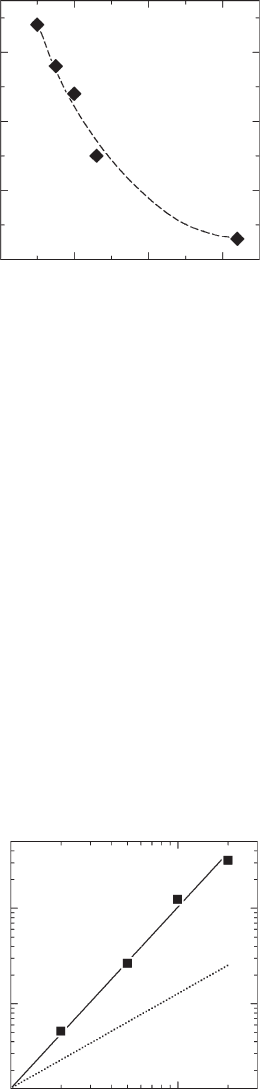
The measured integrated intensity J of the QDSL band in dependence on the number N of the
Ge layers ( Fig. 10.16 ) follows a quadratic dependence J N
2
rather than a linear additive rule
J N . This quadratic dependence was predicted by our calculations [78] . The superlinear beha-
viour indicates the presence of a new recombination mechanism in the studied superlattices. We
believe that it is a more effi cient type-I recombination, which is provided by the electron miniband
in the Ge/Si QDSLs. In other words, the recombination of electron and hole takes place within
30
20
10
81012
0
QDSL period, C (nm)
Miniband width, Δ
MB
(meV)
Figure 10.15 Electron miniband width Δ
MB
versus period C in the QDSL column. Diamonds – value of Δ
MB
calculated on the basis of the experimental data B , W and E
A
using Eq. 10.2 and effective mass of the state density
in Ge/Si QDSL. Dashed line is a guide for the eye.
10
1
12 5
10 20
Integrated PL intensity, J (a.u.)
Number of Ge layers, N
J ~ N
2
J ~ N
Figure 10.16 Room temperature PL integrated intensity of QDSL band ( J ) versus the number N of Ge layers.
Excitation power density – 6 Wcm
2
. Squares – experimental data; solid line is a fi t to the quadratic dependence on
N ; dotted line – linear dependence on N . Both curves converge for N 1 .
CH010-I046325.indd 338CH010-I046325.indd 338 6/27/2008 4:28:50 PM6/27/2008 4:28:50 PM