Leroy C., Rancoita P.-G. Principles Of Radiation Interaction In Matter And Detection
Подождите немного. Документ загружается.


January 9, 2009 10:21 World Scientific Book - 9.75in x 6.5in ws-bo ok975x65˙n˙2nd˙Ed
550 Principles of Radiation Interaction in Matter and Detection
7.1.2 Surface and Total Dose Effects on the Gain Degradation of
Bipolar Transistors
Equation (7.13) accounts for the gain degradation of bipolar transistors when the
atomic displacement is the dominant damage-mechanism. However, it was found
that the gain degradation may result from damages in the silicon lattice and modi-
fications in the surface properties (i.e. the so-called surface effects) of the crystal. For
instance, changes in the recombination properties of surface layers like those close
to the emitter-base junction may affect the transistor current-gain. Surface effects
may occur even at small radiation doses which, usually, are insufficient to introduce
an appreciable bulk damage. Thus, these effects can be investigated with particles of
very large D
Ion
/D
NIEL
ratio between the doses deposited by ionization and atomic
displacement (e.g., see Sect. 4.2.3.1), like γ-rays from a
60
Co source.
This type of damage was considered to be responsible for the observed non-
linear dependence of ∆(1/β) in n − p − n transistors as a function of fluence up to
≈ 10
15
Compton-electron/cm
2∗∗
(e.g., see Figure 60 at page 165 of [Vavilov and
Ukhin (1977)]). These electrons have an average kinetic energy of ≈ 0.53 MeV
and are generated by Compton effect in irradiations with γ-rays from a
60
Co
source
††
. The surface component of the damage grows rapidly and approaches sa-
turation for fluences & 3 × 10
13
Compton-electron/cm
2‡‡
. Above ≈ 10
15
Compton-
electron/cm
2
, the transistor degradation was found to be dominated by the di-
splacement damage as expected from Eq. (7.12). After irradiations with 2 MeV
electrons, a similar behavior is observed for the same type of bipolar transistor
(e.g., see Figure 5.3 at page 215 of [Holmes-Siedle and Adams (2002)]). In irradi-
ations of n − p − n transistors with gamma-rays from
60
Co source up to a dose
of ≈ 0.5 Mrad, the excess base-current was observed to increase non-linearly with
increasing dose
∗
[Nowlin et al. (1993)]. Furthermore, this excess base-current was
observed to saturate at about 1 Mrad, almost independently of the dose rate [Kosier
et al. (1994)]. The linear increase of the inverse of the current gain was observed at
large doses (above 5–10 Mrad) after irradiations with gamma-rays from
60
Co source
and at large fluences (& 10
14
e/cm
2
) with 4.1 MeV electrons [Cheryl, Marshall,
Burke, Summers and Wolicki (1988)].
The so-called lateral and vertical transistors are realized with an architecture
which favors the current flow, mainly, parallel to the surface and in the vertical
direction, respectively. In irradiations with gamma-rays from
60
Co source up to
≈ 0.5 Mrad, a systematic comparison of dose effects on p − n − p transistors has
∗∗
At this Compton-electron fluence, the concentration of initial Frenkel-pairs is ≈ 4.9×10
14
cm
−3
,
for E
d
= (21–25) eV.
††
The ratio of the Compton-electron flux to the flux of γ-rays from the
60
Co source is ≈
0.0162 [Summers, Burke, Shapiro, Messenger and Walters (1993)].
‡‡
At this Compton-electron fluence, the concentration of initial Frenkel-pairs is ≈ 1.5×10
13
cm
−3
,
for E
d
= (21–25) eV.
∗
To deliver a dose of ≈ 100 Mrad, a fluence of ≈ 1.9 × 10
17
γ/cm
2
from a
60
Co source is needed
(e.g., see Figure 5.3 at page 215 of [Holmes-Siedle and Adams (2002)]).

January 9, 2009 10:21 World Scientific Book - 9.75in x 6.5in ws-bo ok975x65˙n˙2nd˙Ed
Displacement Damage and Particle Interactions in Silicon Devices 551
shown that vertical transistors exhibit the least gain degradation [Schimidt et al.
(1995)]. Furthermore, it has been observed that lateral p − n − p transistors with
lightly-doped emitters degrade more rapidly than devices with heavily-doped emit-
ters [Wu et al. (1997)].
Surface and low dose-rate effects in irradiated transistors are discussed, for in-
stance, in Section 6 of Chapter I of Part II of [Vavilov and Ukhin (1977)], [Cheryl,
Marshall, Burke, Summers and Wolicki (1988)], Section 6.14 of [Messenger and Ash
(1992)], Chapter 5 of [Claeys and Simoen (2002)] and Section 5.4 of of [Holmes-
Siedle and Adams (2002)] (see also references therein).
7.1.3 Generalized Messenger–Spratt Equation for Gain Degrada-
tion of Bipolar Transistors
As discussed in Sect. 7.1.1, the Messenger–Spratt equation [Eqs. (7.13, 7.14)] relates
the particle fluence to the variation of the reciprocal of the common-emitter current
gain for particles fluences sufficiently large to allow the displacement damage in
the bulk to be the dominant damage-factor. In Section 4.3.1, we have already dis-
cussed that the concentration of Frenkel-pairs (FP ) is expected to be proportional
to the concentration of deep defects acting as recombination-centers, when these
traps are resulting from primary defects mostly created by cascading-displacement
processes. As a consequence, the variation of the reciprocal of the minority-carrier
lifetime [∆(1/τ
B
)] is expected to depend linearly on FP almost independently of
the type of incoming particle, i.e., to exhibit an approximate NIEL scaling.
Under the assumptions regarding the validity of the Messenger–Spratt equa-
tion (discussed in Sect. 7.1.1) and these latter about the creation mechanism of
recombination centers, we can combine Eqs. (4.131, 7.14) to obtain
∆
µ
1
β
¶
≈
1
ω
T
µ
Φ
i
K
τ,i
¶
= λ
FP
ω
T
, (7.20)
where (as discussed in Sect. 4.3.1) λ is almost independent of the type and energy
of the incoming particle, but depends on the i) the type of substrate, ii) the dopant
concentration (slightly) and iii) the level of compensation. Thus, λ may dep end on
the type (n −p −n or p −n −p) of transistor and VLSI technology (e.g., base width
and doping-profile of the graded base). However, the effect on the gain degrada-
tion [∆(1/β)] is expected to depend almost linearly on FP . Equation (7.20) is the
generalized expression for the common-emitter current gain degradation in bipolar
transistors and it is termed generalized Messenger–Spratt equation
†
[Consolandi,
†
The treatment described in Sect. 4.3.1 and the generalized Messenger–Spratt equation were first
derived by Rancoita et al. in [Colder et al. (2001); Codegoni et al. (2004b); Consolandi, D’Angelo,
Fallica, Mangoni, Modica, Pensotti and Rancoita (2006)] (see also [Leroy and Rancoita (2007)]
and references therein).

January 9, 2009 10:21 World Scientific Book - 9.75in x 6.5in ws-bo ok975x65˙n˙2nd˙Ed
552 Principles of Radiation Interaction in Matter and Detection
D’Angelo, Fallica, Mangoni, Modica, Pensotti and Rancoita (2006)]. This equation
extends the Messenger–Spratt equation (7.13) originally derived for fluences of fast
neutrons. It relates ∆(1/β) to the concentration of Frenkel-pairs created in the si-
licon by the displacement damage and accounted for the energy deposited in NIEL
processes (treated in Sect. 4.2.1). In addition, it predicts that, similarly to ∆(1/τ
B
)
[see discussion in Sect. 4.3.1], ∆(1/β) is expected to follow an approximate NIEL
scaling. Furthermore, Eq. (7.20) can be rewritten as
∆
µ
1
β
¶
≈ k(I
c
) FP (7.21)
with
k(I
c
) =
λ
ω
T
. (7.22)
The first exp erimental evidence of the validity of Eq. (7.20) [Eq. (7.21)] was ob-
tained in irradiations with fast-neutrons with fluences up to ≈ 1.2×10
15
n/cm
2
, with
12
C-ions
¶
of 95.0 MeV/amu up to ≈ 10
13
C/cm
2
and with
13
C-ions of 11.1 MeV/amu
up to ≈ 10
13
C/cm
2
[Colder et al. (2001)] (see also [Colder et al. (2002)]). ∆(1/β)
was found to follow an approximate NIEL scaling over the full range of the gen-
erated concentration of Frenkel-pairs
‡
[(6.4 × 10
13
–1.1 × 10
18
) cm
−3
]. It has to be
noted that for same amount of FPs the D
Ion
(Carbon)/D
Ion
(neutron) dose ratio is
larger than 10
3
(see Table 4.5 and [Consolandi, D’Angelo, Fallica, Mangoni, Mod-
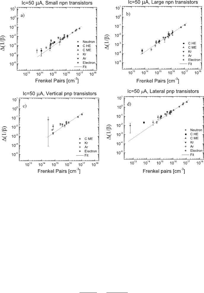
ica, Pensotti and Rancoita (2006)]). Experimental values of ∆(1/β) as a function of
FP are shown in Fig. 7.3 for collector currents of 50 µA. In the figure, the data are
for n − p − n transistors with (a) small and (b) large emitter area, and (c) vertical
and (d) lateral p −n −p transistors
‡‡
manufactured according to the HF2BiCMOS
technology [Gola, Pessina and Rancoita (1990)].
As can be seen in Fig. 7.3, these results have been confirmed in irradiations with
Ar- and Kr-ions [Codegoni et al. (2004b); Consolandi, D’Angelo, Fallica, Mangoni,
Modica, Pensotti and Rancoita (2006)]. Irradiations with 9.1 MeV electrons for flu-
ences up to 2 × 10
15
e/cm
2
have provided a further confirmation of Eq. (7.20) (see
Fig. 7.3) [Codegoni et al. (2006); D’Angelo, Fallica, Galbiati, Mangoni, Modica,
Pensotti and Rancoita (2006)]. In fact, the ratio D
Ion
(electron)/D
Ion
(neutron) of
the ionization dose of electrons with respect to that of fast-neutrons is larger than
four orders of magnitude for the same amount of FP created by displacement da-
mage (see Table 4.5 and [Consolandi, D’Angelo, Fallica, Mangoni, Modica, Pensotti
and Rancoita (2006)]). It has to be noted that, as discussed in Sect. 4.2.1.4, the recoil
silicon is able to produce a small cascade development for incoming electrons with
¶
The reader can find the definition of kinetic energies per amu in Sect. 1.4.1.
‡
The concentrations of Frenkel-pairs for C-ions were computed by means of the TRIM simulation
code [Ziegler, Biersack and Littmark (1985a); Ziegler (2001)] and for fast-neutrons by the data
available in literature for the damage function (e.g., see Sect. 4.2.1.5).
‡‡
The devices were characterized using an HP4142B modular DC source-monitor and the IC-CAP
code (version 2004 [IC-CAP (2004)] or previous versions) controlled by a workstation.
January 9, 2009 10:21 World Scientific Book - 9.75in x 6.5in ws-bo ok975x65˙n˙2nd˙Ed
Displacement Damage and Particle Interactions in Silicon Devices 553
Fig. 7.3 ∆(1/β) as a function of the concentration of Frenkel-pairs (FP ) (from [Leroy and Ran-
coita (2007)]; see also [Consolandi, D’Angelo, Fallica, Mangoni, Modica, Pensotti and Rancoita
(2006)]): for n − p − n transistors with (a) small [5 µm ×5 µm] and (b) large [50 µm ×50 µm]
emitter area, and for (c) vertical and (d) lateral p − n − p transistors manufactured according
to the HF2BiCMOS technology [Gola, Pessina and Rancoita (1990)]. The collector current is
50 µA. The incoming particles are fast-neutrons,
12
C-ions of 95.0 MeV/amu (high-energy),
13
C-
ions of 11.1 MeV/amu (medium-energy),
36
Ar-ions of 13.6 MeV/amu,
86
Kr-ions of 60.0 MeV/amu
and electrons of 9.1 MeV [Colder et al. (2001, 2002); Codegoni et al. (2004b, 2006); Consolandi,
D’Angelo, Fallica, Mangoni, Modica, Pensotti and Rancoita (2006); D’Angelo, Fallica, Galbiati,
Mangoni, Modica, Pensotti and Rancoita (2006)]. The line represents the linear dependence ex-
pected from Eq. (7.20).
this kinetic energy. Furthermore, for any value of the collector current, the slope
of the fitted straight-line to ∆(1/β) as a function of FP [e.g., see Eqs. (7.21, 7.22)]
determines the quantity k(I
c
) and, thus, the value of
f
T
(I
C
)
λ
=
1
2 π k(I
c
)
(7.23)
as a function of the collector current [e.g., see Eq. (7.19)]. f
T
(I
C
)/λ as a function of
I
C
is shown in Fig. 7.4 for the irradiated n −p −n and p −n −p transistors. These
curves indicate that i) the cutoff frequencies reach their maxima above 100 µA as
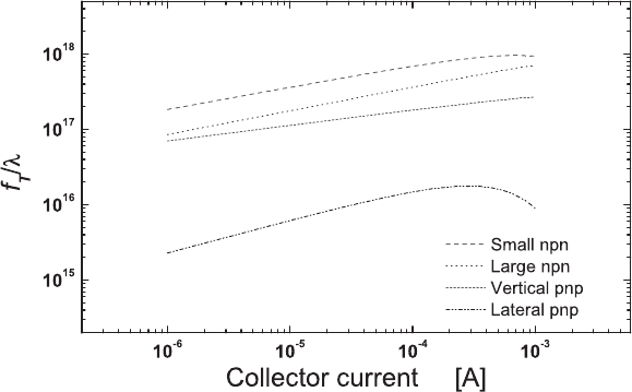
January 9, 2009 10:21 World Scientific Book - 9.75in x 6.5in ws-bo ok975x65˙n˙2nd˙Ed
554 Principles of Radiation Interaction in Matter and Detection
Fig. 7.4 f
T
(I
C
)/λ as a function of the collector current (in A) [see Eq. (7.23)] (adapted from
[Leroy and Rancoita (2007)]; see also [Consolandi, D’Angelo, Fallica, Mangoni, Modica, Pen-
sotti and Rancoita (2006)]): for n − p − n transistors with (a) small [5 µm ×5 µm] and (b) large
[50 µm ×50 µm] emitter area, and for (c) vertical and (d) lateral p −n −p transistors manufactured
according to the HF2BiCMOS technology [Gola, Pessina and Rancoita (1990)].
expected in this technology [Gola, Pessina and Rancoita (1990)] and ii) their ratios
are in agreement with those expected for the different types of transistors in this
technology [e.g., ≈ 20 MHz for lateral p − n − p transistors versus (2–6) GHz for
n − p − n transistors]. It has to be noted that below ≈ 100 µA (e.g., see [Colder et
al. (2001); Consolandi, D’Angelo, Fallica, Mangoni, Modica, Pensotti and Rancoita
(2006)]), k(I
c
) can be approximated by
k(I
c
) = A
tr
I
n
c
, (7.24)
where A
tr
and n depend on the type of transistor. The values found for the coefficient
n are ≈ −(0.2–0.4) [Leroy and Rancoita (2007)] (see also [Consolandi, D’Angelo,
Fallica, Mangoni, Modica, Pensotti and Rancoita (2006)]) and are in agreement with
those available in literature (e.g., see Section 7 of Chapter 1 of Part II in [Vavilov
and Ukhin (1977)]).
In summary, these experimental data indicate that, at large values of FP , the
dominant processes resulting in gain degradation are well accounted by the processes
of non-ionization energy-loss.
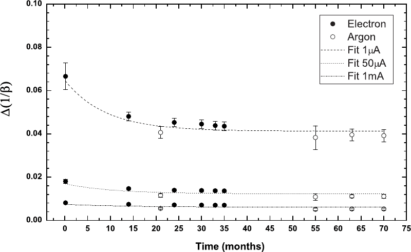
7.1.4 Transistor Gain and Self-Annealing
The defects induced by radiation, as discussed in Sect. 4.2.2, may be unstable and,
thus, their concentration may decrease with time. For instance (e.g., see Sect. 4.3.1),
an annealing effect was observed for the lifetime of minority-carriers, thus decreasing

January 9, 2009 10:21 World Scientific Book - 9.75in x 6.5in ws-bo ok975x65˙n˙2nd˙Ed
Displacement Damage and Particle Interactions in Silicon Devices 555
the value of K
τ,n
(see pages 32–45 in [Srour, Long, Millward, Fitzwilson and Chad-
sey (1984)], also [Srour (1973)] and references therein). Therefore, the annealing is
expected to cause the (slight) increase of the current gain of the bipolar transistors.
To a first approximation, this gain increase exponentially approaches a constant
value with time.
The annealing effect on ∆(1/β) for large emitter area n−p−n transistors [Gola,
Pessina and Rancoita (1990)] has been investigated, at 25
◦
C, from immedia-
tely after the (electron) irradiation up to about 70 months after Argon irradi-
ation [Codegoni et al. (2004b); Rancoita (2005); Consolandi, D’Angelo, Fallica,
Mangoni, Modica, Pensotti and Rancoita (2006); Leroy and Rancoita (2007)] and
is shown in Fig. 7.5 for three values of the collector currents: 1 µA, 50 µA and
1 mA. The irradiations with electrons of 9.1 MeV (2 ×10
15
e/cm
2
) and
36
Ar-ions of
13.6 MeV/amu (10
11
Ar/cm
2
) created initially a concentration ≈ 7.2 × 10
15
cm
−3
of Frenkel-pairs. The data show that i) there is evidence for a long-term annealing
with a decay time of (10.0 ± 2.98) months and ii) the effect of annealing is similar
for devices irradiated with electrons and Ar-ions [Consolandi, D’Angelo, Fallica,
Mangoni, Modica, Pensotti and Rancoita (2006)].
7.1.5 Radiation Effects on Low-Resistivity Base Spreading-
Resistance
The bipolar transistors have a wide range of circuit applications, for example as
input device in fast front-end electronics
††
. However, the degradation of transi-
stor properties resulting from radiation damage may impair the expected opera-
tion of the whole electronic circuit. In Sections 7.1.1, 7.1.3, we have discussed
the decrease of the gain and the increase of the base current of bipolar transi-
stors with increasing fluence. Furthermore from the base lead, a current must flow
through the graded-base region up to the recombination centers, the emitter-base
junction and, also, the emitter region: the overall resistance, involving different
parts of the base region, is referred to as base spreading-resistance {e.g., see Sec-
tion 16.4(d) of [van der Ziel (1976)], Section 7.2 of [M¨uller and Kamins (1977)] and
Section 14.4(c) of [Bar-Lev (1993)]}: the displacement damage may also cause a
variation of the effective-doping concentration in the base. In high-resistivity de-
vices (e.g., silicon radiation detectors), the resistivity is largely modified by irradi-
ation (see Sects. 4.3.4, 4.3.5, 6.8.3). As the doping concentrations used in bipolar
transistors are several orders of magnitude larger, the radiation-induced change in
doping concentration is usually less important, but may not be negligible at large
fluences. For instance when these transistors (see Section 5.1.2 of [Gatti and Man-
fredi (1986)]) are employed as input stage of charge-sensitive-preamplifier (CSP),
the increase of transistor base-current and slight variation of the effective doping-
††
The reader may see, e.g., [Gatti and Manfredi (1986); Gola, Pessina and Rancoita (1990); Gola,
Pessina, Rancoita, Seidman and Terzi (1992); Baschirotto et al. (1997)] and references therein.
January 9, 2009 10:21 World Scientific Book - 9.75in x 6.5in ws-bo ok975x65˙n˙2nd˙Ed
556 Principles of Radiation Interaction in Matter and Detection
Fig. 7.5 Annealing effect at 25
◦
C: dependence of ∆(1/β) for large emitter-area transistors [Gola, Pessina and Rancoita (1990)] on the time (in
months) after irradiation with electrons (2 × 10
15
e/cm
2
) and Ar-ions (10
11
Ar/cm
2
) (adapted from [Leroy and Rancoita (2007)]; see also [Rancoita
(2005); Consolandi, D’Angelo, Fallica, Mangoni, Modica, Pensotti and Rancoita (2006)]). The initial concentration of Frenkel-pairs is ≈ 7.2 ×
10
15
cm
−3
. The lines show the fitted curves for collectors currents exponentially decreasing with time. The currents are 1 µA (dashed line), 50 µA
(dotted line) and 1 mA (dashed and dotted line), respectively.
January 9, 2009 10:21 World Scientific Book - 9.75in x 6.5in ws-bo ok975x65˙n˙2nd˙Ed
Displacement Damage and Particle Interactions in Silicon Devices 557
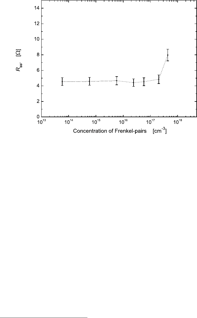
Fig. 7.6 R
bb
0
(in Ω) as a function of the concentration of Frenkel-pairs (in cm
−3
) (adapted from
[Leroy and Rancoita (2007)]; see also [Baschirotto et al. (1997)]). The line is to guide the eye.
concentration of the base spreading-resistance (R
bb
0
) are among the relevant causes
of degradation of parallel and series noise of the CSP. This occurs even with very
short (≈ 20 ns) shaping-times
∗∗
.
The values of R
bb
0
for n −p −n bipolar transistors, manufactured according to
VLSI technology in HF2BiCMOS process [Gola, Pessina and Rancoita (1990)], were
determined after irradiation with fast-neutrons up to a fluence of ≈ 9××10
15
n/cm
2
by measuring the noise performance of CSPs with these devices employed as in-
put stage [Baschirotto et al. (1997)]: they are shown in Fig. 7.6 as a function
of the concentration of the Frenkel-pairs (FP ) created during irradiation [Leroy
and Rancoita (2007)]. R
bb
0
is compatible with the value before irradiation up to
FP ≈ 6 × 10
16
cm
−3
and is ≈ (70–75)% larger at the largest fluence, i.e., for
FP ≈ 4.3 × 10
17
cm
−3
, in agreement (see discussion in [Baschirotto et al. (1997)])
with data available in literature (e.g., see Section 5.13 of [Messenger and Ash
(1992)]).
Furthermore, R
bb
0
is proportional to the base resistivity, thus to the reciprocal
of the carrier mobility [Eq. (6.19)]. For the p- (n-) type base, the mobility µ
p
(T )
∗∗
The reader can refer, for instance, to [Baschirotto et al. (1993, 1995a,b, 1996, 1997, 1999)] and
references therein.

January 9, 2009 10:21 World Scientific Book - 9.75in x 6.5in ws-bo ok975x65˙n˙2nd˙Ed
558 Principles of Radiation Interaction in Matter and Detection
[µ
n
(T )] is given
†
by [Arora, Hauser and Roulston (1982)]:
µ
p
(T ) = 54.3 × T
−0.57
r
+
1.36 × 10
8
× T
−2.23
1 + 0.88 × T
−0.146
r
{N
a
/ [2.35 × 10
17
× T
2.4
r
]}
, (7.25)
µ
n
(T ) = 88.0 × T
−0.57
r
+
7.4 × 10
8
× T
−2.33
1 + 0.88 × T
−0.146
r
{N
d
/ [1.26 × 10
17
× T
2.4
r
]}
, (7.26)
where T is the temperature (in kelvin) and T
r
= T/300; N
a
(N
d
) is effective
dopant concentration in the p- (n-) type base. Before and after irradiation with
the largest fluence (see [Baschirotto et al. (1997)]), the (p-type) base spreading-
resistance was also determined as a function of the temperature T in the range
283 < T < 343 K. The temperature dependence of R
bb
0
was observed to be de-
termined by values of µ
p
(T ) compatible with those calculated using Eq. (7.25) for
dopant concentration of ≈ 10
18
cm
−3
before irradiation, i.e., with that employed for
the base in this technology, and ≈ 5×10
17
cm
−3
after the largest irradiation [Baschi-
rotto et al. (1997)].
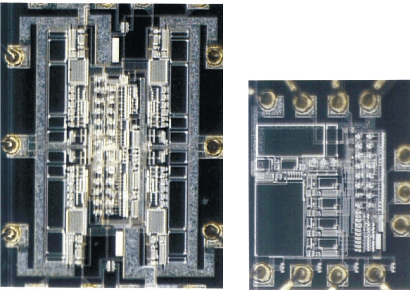
In Fig. 7.7, a radiation hard fast bipolar monolithic charge sensitive preamplifier
(CSP) and its associated monolithic shaper (with 20 ns shaping time) are shown:
both devices are implemented in HF2BiCMOS technology.
7.2 Single Event Effects
As already mentioned, a Single Event Effect (SEE) is due to an individual event
caused by a heavy-ion (i.e., a single charged particle with Z ≥ 2) traversing a semi-
conductor or semiconductor-based device (integrated circuit, power supply, etc.). A
SEE results in a failure of the device. This failure is the consequence of the charge
deposition resulting from the electron-hole pairs generated along the path of the
incoming particle within the sensitive volume of the device (direct ionization). SEE
can also be caused by the interactions (elastic, inelastic scattering or spallation)
of the incoming particle, neutron or proton, with atoms in the device producing
light particles such as protons, deuterons, α-particles, light nuclei such as lithium,
beryllium and heavy recoil nuclei such as magnesium. Most of the recoil species are
heavier than the original particle and have large ionization capabilities. Then, the
recoil particles can also generate tracks of electron-hole pairs along their path (in-
direct ionization). The charge deposition mechanisms are the same as in the case of
directly ionizing ions. In both situation, the energy deposition via direct or indirect
ionization creates electric charges which, if enough electric charge is created, may
modify the functional state of the device, leading to errors. The minimum electric
charge that causes the change of state in the device is called the critical charge (Q
c
)
and a SEE occurs if the collected charge exceeds Q
c
. The critical charge is formed
†
These expressions agree (within ±13%) with experimental data in the temperature range (250–
500) K and up to a dopant concentration of ≈ 10
20
cm
−3
(for additional data see [Arora, Hauser
and Roulston (1982)] and references therein).
January 9, 2009 10:21 World Scientific Book - 9.75in x 6.5in ws-bo ok975x65˙n˙2nd˙Ed
Displacement Damage and Particle Interactions in Silicon Devices 559
Fig. 7.7 (left) Photograph of a monolithic CSP: four preamplifiers are located on a single die, sharing the biasing network; the chip dimension
is 1.62 × 1.17mm
2
. (right) Photograph of the monolithic shaper associated to the CSP: the circuit area is 1.08 × 0.93 mm
2
. The photographs are
reprinted from Nucl. Instr. and Meth. in Phys. Res. B 155, Baschirotto A. et al., A radiation hard bipolar monolithic front-end readout, 120–131,
Copyright (1999), with permission from Elsevier, e.g., for the list of the authors see [Baschirotto et al. (1999)].