Leroy C., Rancoita P.-G. Principles Of Radiation Interaction In Matter And Detection
Подождите немного. Документ загружается.


January 9, 2009 10:21 World Scientific Book - 9.75in x 6.5in ws-bo ok975x65˙n˙2nd˙Ed
540 Principles of Radiation Interaction in Matter and Detection
matic investigations for low- and high-resistivity silicon.
The particle interactions in the bulk or active volume of silicon devices are
responsible for the device degradation resulting from the absorbed dose
∗
and the
so-called single event phenomena
††
.
As mentioned in Sects. 4.2.3.1, 4.2.3.2, the energy deposited by ionization or
collision energy-loss processes accounts for the largest fraction of the total energy
deposited in any medium (e.g., in a silicon semiconductor). Silicon based devices
are affected by the total (i.e., and by far, ionizing) absorbed dose: for instance in
MOS transistors, shifts of the threshold voltage and variations of the sub-threshold
slope occur.
Other silicon based devices, like solar cells (Sect. 6.6) and bipolar transi-
stors, are mostly affected by the displacement damage generated by non-ionizing
energy-loss processes (e.g., see [Srour, Marshall and Marshall (2003)] and references
therein). For instance, at large cumulative irradiations this mechanism was found to
be responsible i) for the decrease of the gain of bipolar transistors
‡‡
mostly as a result
of the decrease of the minority-carrier lifetime (e.g., see Sect. 4.3.1) in the transistor
base and ii) for the degradation of the series-noise performance of charge-sensitive-
preamplifiers with bipolar junction transistors in the input stage mainly because of
the increase of the base spreading-resistance (e.g., see Sects. 4.3.5, 7.1.5) of these
transistors
∗∗
. Furthermore, through systematic measurements (see Sects. 7.1, 7.1.3)
it was found that the gain degradation of bipolar transistors manufactured on VLSI
technologies depends almost linearly on the amount of displacement damage gener-
ated (e.g., the amount of energy deposited by NIEL processes) independently of the
type of incoming particle [Colder et al. (2001, 2002); Codegoni et al. (2004a,b, 2006);
Consolandi, D’Angelo, Fallica, Mangoni, Modica, Pensotti and Rancoita (2006);
D’Angelo, Fallica, Galbiati, Mangoni, Modica, Pensotti and Rancoita (2006)].
A Single Event Effect (SEE) is due to an individual event caused by a single
charged particle (Z ≥ 2) traversing a semiconductor or semiconductor-based device
(e.g., integrated circuit, power supply, etc.). A SEE results in a failure of the device,
as a consequence of the charge deposited along the path of the incoming particle
∗
Both the non-ionizing (e.g., see Sect. 4.2.1) and ionizing (e.g., see Sect. 4.2.3) energy-losses
contribute to the absorbed dose. The reader can see, for instance, [Vavilov and Ukhin (1977);
Srour, Long, Millward, Fitzwilson and Chadsey (1984); Ma and Dressendorfer (1989); Messenger
and Ash (1992); Claeys and Simoen (2002); Holmes-Siedle and Adams (2002); ECSS (2005)],
Sect. 7.1 and references therein.
††
One can see, e.g., [Srour, Long, Millward, Fitzwilson and Chadsey (1984); Messenger and Ash
(1992, 1997); Claeys and Simoen (2002); Holmes-Siedle and Adams (2002); ECSS (2005)], Sect. 7.2
and references therein.
‡‡
The reader can refer, e.g., to [Frank and Larin (1965); Messenger (1966); Ramsey and Vail (1970);
Messenger (1972); Srour (1973); Vavilov and Ukhin (1977); Srour, Long, Millward, Fitzwilson and
Chadsey (1984); Srour and McGarrity (1988); Srour and Hartman (1989); Messenger and Ash
(1992); Colder et al. (2001, 2002); Codegoni et al. (2004a,b); ECSS (2005); Codegoni et al. (2006);
Consolandi, D’Angelo, Fallica, Mangoni, Modica, Pensotti and Rancoita (2006)] and references
therein.
∗∗
A discussion can be found, e.g., in [Baschirotto et al. (1995a,b, 1996, 1997, 1999)] and references
therein.

January 9, 2009 10:21 World Scientific Book - 9.75in x 6.5in ws-bo ok975x65˙n˙2nd˙Ed
Displacement Damage and Particle Interactions in Silicon Devices 541
within the sensitive volume of the device. SEE’s are treated in Sects. 7.2–7.2.8.
Substantial progress has been made in the understanding of mechanisms at the
origin of SEE and predicting their rate of occurrence for various types of devices
and circuits. Monte Carlo tools have been developed which take into account the
evolution of modern technology toward faster devices with less power consumption
and denser circuits increasingly small. This reduction in size and multiplication of
active cells lead to a re-examination of the concepts of critical charge and sensitive
volume. The RPP approximation for the sensitive volume, although convenient for
rapid estimates, has to be much more refined to account for effects such as funneling,
bipolar effects, source-to-drain currents. These effects are the source of sensitivity
variations across the devices, not easily reproducible by Monte Carlo. The use of
powerful simulation to ols such as GEANT4 allows the accurate description of the
device geometry, structure, material composition, and at the same time the inclusion
of the mechanisms of energy deposition, and cell charge collection efficiency. SEE
cross sections for specific species of particles and ions are measured at accelera-
tors and can be convoluted with effective LET spectrum calculated by GEANT4
to infer SEE rates. These predictions are strictly viable for the experimental con-
ditions under which the cross sections have been measured. The ultimate goal is
to extend these predicted SEE rates beyond these specific conditions and rely only
on GEANT4 fed with refined models of energy deposition and charge collection
efficiency in the various regions of the device in order to calculate the charge col-
lected which also depends on the time constant of the process. This also supposes
that progress will be made in the determination of the sensitive volume size and
shape and of the critical energy which remain a major uncertainty in Monte Carlo
simulations. Precise SEE rate predictions may then have a strong impact on device
design.
7.1 Displacement Damage in Irradiated Bipolar Transistors
The bipolar transistor
∗
(contraction for transfer resistor) consists of two successive
junctions (n − p − n, or p − n − p) made by three semiconductor regions called
emitter (heavily doped
†
), base and collector, respectively. It is one of the most im-
portant semiconductor components available, nowadays, on VLSI (Very Large Scale
∗
A general treatment of this topic can be found, e.g., in Chapter 7 of [Grove (1967)], Chapter 6
of [M¨uller and Kamins (1977)], Chapter 4 of [Sze (1985)], Sections 3.9–3.14 of [Messenger and Ash
(1992)], Chapter 10 of [Neamen (2002)] and also [Sze (1981); Goodge (1983); Bar-Lev (1993); Ng
(2002); M¨uller and Kamins - with Chan (2002); Brennan (2005)].
†
In VLSI technologies, the emitter- and base-regions are strongly graded with doping concentra-
tions which may exceed 10
20
and 10
18
cm
−3
, respectively; while the collector-region is typically an
epitaxial-layer [Sze (1988)] with dopant concentration lower than 10
16
cm
−3
(e.g., see Figs. 6.16
and 6.17 at page 304 of [M¨uller and Kamins (1977)], Fig 11 at page 25 of [Sze (1985)] and Fig 3.27
at page 133 of [Messenger and Ash (1992)] 2nd Edition).

January 9, 2009 10:21 World Scientific Book - 9.75in x 6.5in ws-bo ok975x65˙n˙2nd˙Ed
542 Principles of Radiation Interaction in Matter and Detection
Integration) technologies. It was invented
‡
by a research team at Bell Laboratories
in 1947 (see page 133 of [Sze (1981)]). In this device, both the electrons and holes
§
participate in the conduction mechanism.
The emitter-base junction is forward-biased and, consequently, allows a large
injection into the base-region of minority (for the base) carriers, which are majority
carriers inside the emitter-region. The base-collector junction is reverse-biased and
sufficiently close to the emitter-base junction so that most of these carriers can
reach the collector-region, where they are carriers of the majority type. Thus, in
the bipolar transistor operation, a large current flows in the reverse-biased base-
collector junction due to the large injection of carriers coming from the forward-
biased emitter-base junction in its vicinity. Since not all the injected carriers from
the emitter will reach the collector-region, two quantities are of great importance
in describing the d.c. transistor characteristics
∗
:
a) the so-called base-transport factor given by
α
T
≡
I
C,m
I
E,m
, (7.1)
where I
C,m
is the current due to the minority (in the base-region, but majority in
the emitter-region from which they are injected) carriers reaching the collector and
I
E,m
is that due to the minority carriers initially injected from the emitter into the
base;
b) the current gain given by
β
0
≡
I
C
I
B
, (7.2)
where I
C
and I
B
are the collector and base current, respectively. The collector cur-
rent accounts for the carriers, which are capable to reach the collector after passing
through the base region. The base current accounts for recombination processes in
the base, recombination in the emitter-base region and diffusion of carriers from the
base into the emitter region. The minority-carrier flow [see Eq. (7.1)] provides the
basic mechanism of the transistor operation and, as a consequence, of its degrada-
tion under irradiation.
In circuit applications, the most often configuration of transistors is the so-
called common-emitter configuration under active mode, that is, the emitter lead
is common to the input and output circuits, the emitter-base junction is forward-
biased and the base-collector junction is reverse-biased. The collector current can
be written as {see Equation (46) at page 128 of [Sze (1985)]}:
I
C
= β I
B
+ I
C,o
, (7.3)
‡
In 1948 J. Bardeen and W. Brattain announced the development of the point contact transi-
stor [Bardeen and Brattain (1948)], while in 1949 W. Shockley published his paper on junction
diodes and transistors [Shockley (1949)]: all of whom subsequently won the Nobel Prize in Physics
in 1956.
§
This is the reason why is called bipolar.
∗
For a general treatment of the bipolar transistor properties, one may refer, for instance, to
Chapter 7 of [Grove (1967)], Chapter 6 of [M¨uller and Kamins (1977)], Chapter 4 of [Sze (1985)]
and Chapter 10 of [Neamen (2002)].
January 9, 2009 10:21 World Scientific Book - 9.75in x 6.5in ws-bo ok975x65˙n˙2nd˙Ed
Displacement Damage and Particle Interactions in Silicon Devices 543
where I
C,o
is the collector-emitter leakage current with open base and β is the
so-called common-emitter current gain
¶
. Under the assumption that the recom-
bination current in the emitter-base depletion region is negligible, β is given by
{e.g., see Equations (8) at page 115 and (44) at page 127 of [Sze (1985)]}:
β '
γ α
T
1 − γ α
T
, (7.4)
where γ = I
E,m
/I
E,d
is the so-called emitter efficiency
k
and I
E,d
accounts for the
electron- and hole-current diffusing across the emitter-base junction, e.g., I
E,m
and
the diffusion current due to carriers injected from the base into the emitter region. γ
measures the injected current due to minority carriers with respect to the overall
current due to diffusion from the emitter and base regions. For silicon transistors
at normal temperature of operation, I
C,o
is negligible (e.g, see page 250 in [Bar-Lev
(1993)]) and, thus, from Eqs. (7.2, 7.3), we have β
0
≈ β. Furthermore, for good
transistors we have γ ≈ 1 and α
T
≈ 1 (e.g., see page 156 of [Lutz (2001)]); as a
consequence, since γ α
T
. 1, β
0
is usually large.
In active mode and for low-level injection
∗∗
, under the assumptions that the
transistor has i) uniform doping in each region, ii) no generation-recombination
currents in the depletion regions and iii) neglecting any series resistance in the
device, we obtain {e.g., see Equation (36) at page 121 of [Sze (1985)]}:
α
T
≈ 1 −
W
2
B
2 L
2
B
for
W
B
L
B
¿ 1, (7.5)
where W
B
is the depth of the quasi-neutral base-region
††
and L
B
is the diffusion
length of the minority-carrier in the base. For the usually well-made (and so-called)
narrow-base transistors, the condition W
B
/L
B
¿ 1 is satisfied. L
2
B
is given by the
minority-carrier life-time (τ
B
) multiplied by the diffusion constant (D
B
) of these
carriers [see Eqs. (6.63, 6.64)]. If the emitter efficiency is close to unity (as it is
usual the case), the common-emitter current gain [Eq. (7.4)] can be re-expressed
using Eq. (7.5) as:
β '
α
T
1 − α
T
'
1
1 − α
T
= 2
µ
L
B
W
B
¶
2
. (7.6)
¶
This parameter is indicated as h
fe
, when representing the transistor performance within the
framework of small-signal models for low and high frequencies (e.g., see Section 2.2.26 of [Goodge
(1983)] and Chapter 15 of [Bar-Lev (1993)]); the static common-emitter current gain is also in-
dicated as h
FE
in the h-parameter representation (e.g., see Section 3.2.2 of [Sze (1981)] and Sec-
tion 2.2.17 of [Goodge (1983)]). Furthermore, it is indicated as β
F
, i.e., is the so-called forward
common-emitter current gain within the framework of the Ebers–Moll model (e.g., see the Sec-
tion 14.3(d) of [Bar-Lev (1993)]).
k
The term γ α
T
is the so-called d.c. common-base current gain {e.g., see Equation (4.36) at
page 86 of [Brennan (2005)]}.
∗∗
The condition for low-level injection is satisfied when the excess carrier concentration is small
in comparison with the doping concentration.
††
It extends from the edge of the depletion region of the emitter-base junction to that of the
base-collector junction.

January 9, 2009 10:21 World Scientific Book - 9.75in x 6.5in ws-bo ok975x65˙n˙2nd˙Ed
544 Principles of Radiation Interaction in Matter and Detection
For graded-base transistors, Eq. (7.5) is replaced by the Gover–Grinberg–Seidman
expression {Equation (9) of [Gover, Grinberg and Seidman (1972)], see also [Mes-
senger (1973)]}, which is valid for the case of a general impurity distribution:
α
T
≈ 1 − u
1
µ
W
B
L
B
¶
2
+ u
2
µ
W
B
L
B
¶
4
− . . . , (7.7)
where the coefficients u
i
depend on the base doping-profile
‡
.
For W
B
/L
B
¿ 1, the right side of Eq. (7.7) converges rapidly and the terms
beyond the first two can be neglected {e.g., see Equation (31) of [Gover, Grinberg
and Seidman (1972)]}. Thus, for γ ≈ 1 the common-emitter current gain can be
rewritten using of Eqs. (7.4, 7.7) as:
β '
α
T
1 − α
T
'
1
1 − α
T
= u
1
µ
L
B
W
B
¶
2
. (7.8)
7.1.1 Gain Degradation of Bipolar Transistors and Messenger–
Spratt Equation
Since mid-fifties, the effect of fast-neutron irradiations on bipolar transistor was ex-
tensively investigated by many authors (e.g., see [Webster (1954); Loferski (1958);
Messenger and Spratt (1958); Frank and Larin (1965); Messenger (1967a); Ramsey
and Vail (1970); Messenger (1973); Vavilov and Ukhin (1977); Messenger and Ash
(1992); Codegoni et al. (2004b); Consolandi, D’Angelo, Fallica, Mangoni, Modica,
Pensotti and Rancoita (2006)]). It was shown that the knowledge of the degradation
of the minority carrier lifetime allows one to predict changes in the parameters of
transistors as a function of the fast-neutron fluence: for instance, Webster, Loferski,
Messenger and Spratt could determine that the variation of the reciprocal of the
common-emitter current gain (β) linearly depends on the fast-neutron fluence [Web-
ster (1954); Loferski (1958); Messenger and Spratt (1958)]).
As teated in Sect. 7.1, β
†
[Eq. (7.3)] is related to the lifetime of the minority
carriers in the base as shown by the approximate expression (7.17): the decrease of
their lifetime with increasing fluence (see Sect. 4.3.1) is the fundamental mechanism
which determines the degradation of the transistor gain.
‡
For instance (see Appendices VII and VIII of [Gover, Grinberg and Seidman (1972)]), for a
homogeneous doping-profile in the base we have
u
1
=
1
2
;
while, for an exponential doping-profile of the type N = N
0
exp(−ηx/W
B
) we get
u
1
=
η + exp(−η) − 1
η
2
.
†
As discussed at page 543, in practice the common-emitter current gain does not differ from the
current gain β
0
[Eq. (7.2)], thus the two quantities are used with no distinction in Sects. 7.1.1–7.1.5.
January 9, 2009 10:21 World Scientific Book - 9.75in x 6.5in ws-bo ok975x65˙n˙2nd˙Ed
Displacement Damage and Particle Interactions in Silicon Devices 545
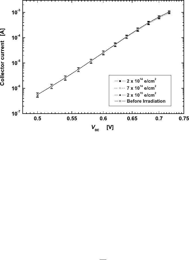
Fig. 7.1 Collector currents (I
C
, in A) measured at 25
◦
C as a function of the voltage (in V)
applied at the emitter-base junction (V
BE
), before and after irradiation with 9.1 MeV electrons
for fluences of 2 × 10
14
, 7 × 10
14
and 2 × 10
15
e/cm
2
(from [Leroy and Rancoita (2007)]; see
also [Consolandi, D’Angelo, Fallica, Mangoni, Modica, Pensotti and Rancoita (2006)]).
Let us consider a transistor with narrow-base (i.e., with W
B
/L
B
¿ 1) with
a graded doping-profile. As mentioned in Sect. 7.1, when this transistor has a
large gain, an emitter efficiency close to 1 and is operated in the common-emitter
configuration under active mode, the base transport factor is approximated by
Eq. (7.7). Furthermore, it is the dominant factor compared to the common-emitter
current gain [see Eqs. (7.4, 7.8)]. Under these assumptions and before irradiation,
β can be approximated by the ratio between the minority-carrier lifetime τ
B
and
the transit time across the base τ
tr
[Eq. (7.17)]. Since τ
tr
is the largest contribution
to the overall emitter-collector delay time (τ
d
), i.e., τ
d
≈ τ
tr
, the cutoff angular
frequency is roughly given by
ω
T
≈
1
τ
tr
. (7.9)
By combining Eqs. (7.17, 7.19), we have, finally,
β ≈ τ
B
ω
T
. (7.10)
After irradiation with fast neutrons, assuming that the transistor retains a signif-
icant common-emitter gain β
irr
(e.g., β
irr
& 3 [Messenger (1973)]) and that the
January 9, 2009 10:21 World Scientific Book - 9.75in x 6.5in ws-bo ok975x65˙n˙2nd˙Ed
546 Principles of Radiation Interaction in Matter and Detection
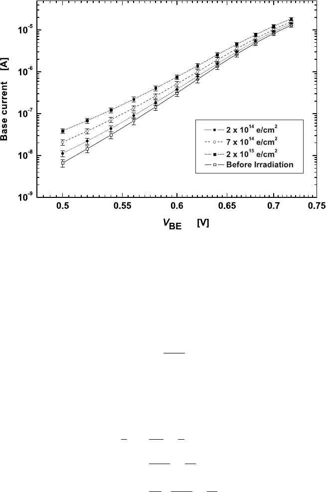
Fig. 7.2 Base currents (I
B
, in A) measured at 25
◦
C as a function of the voltage (in V) applied to
the emitter-base junction (V
BE
), before and after irradiation with 9.1 MeV electrons for fluences
of 2 ×10
14
, 7 ×10
14
and 2 ×10
15
e/cm
2
(from [Leroy and Rancoita (2007)]; see also [Consolandi,
D’Angelo, Fallica, Mangoni, Modica, Pensotti and Rancoita (2006)]).
diffusion constant (D
B
) of the minority carriers in the base does not vary apprecia-
bly, τ
tr
is almost constant [e.g., see Eq. (7.15)]. Thus, β
irr
can be written as
β
irr
≈
τ
B,irr
τ
tr
≈ τ
B,irr
ω
T
, (7.11)
where τ
B,irr
is the lifetime of the minority carriers after irradiation. Then, the vari-
ation of the reciprocal of the common-emitter current gain becomes
∆
µ
1
β
¶
≡
1
β
irr
−
1
β
≈
τ
tr
τ
B,irr
−
τ
tr
τ
B
=
1
ω
T
µ
1
τ
B,irr
−
1
τ
B
¶
. (7.12)
As discussed in Sect. 4.3.1, the variation of the reciprocal of the lifetime of the
minority-carriers in the base is related to the fast-neutron fluence and the lifetime

January 9, 2009 10:21 World Scientific Book - 9.75in x 6.5in ws-bo ok975x65˙n˙2nd˙Ed
Displacement Damage and Particle Interactions in Silicon Devices 547
constant damage; thus, using Eq. (4.125), Eq. (7.12) can be rewritten as:
∆
µ
1
β
¶
≈
1
ω
T
∆
µ
1
τ
B
¶
=
Φ
n
ω
T
K
τ,n
, (7.13)
where K
τ,n
is the lifetime damage coefficient and Φ
n
is the fast-neutron fluence
(e.g., see Sect. 4.3.1).
Equation (7.13) is the Messenger–Spratt equation
‡
, which was initially proven
for homogeneous base transistors [Messenger and Spratt (1958)], later extended to
treat exponentially graded base transistors [Messenger (1967a)] and, finally, using
the Gover–Grinberg–Seidman expression [Eq. (7.7)] generalized to cover any base
doping-profile [Messenger (1973)]. Messenger (1973) has also noted that i) Ramsey
and Vail have shown how the emitter efficiency contribution, resulting from the
effect of recombination processes in the emitter-base field-region, is related to the
emitter time-constant τ
E
[Ramsey and Vail (1970)], ii) Eq. (7.9) is strictly related to
the cutoff angular frequency for the base transport, but iii) ω
T
can be extended by
adding the emitter time constant. Thus, by means of this latter re-expressed value
of ω
T
, Eq. (7.13) accounts for recombination processes in both the emitter-base
field-region and the base (bulk) region.
As discussed in Sect. 4.3.1, the lifetime damage coefficient (K
τ,i
) and Φ
i
de-
pends on the typ e and energy of the incoming particle. Thus, for the same type of
transistor, by inspection of Eqs. (4.125, 7.13) we can see that the variation of the
reciprocal of the current gain (or any quantity proportional to it) is expected to
exhibit different slopes
§
if irradiated with different types of particle. This behavior
was experimentally determined, for instance, by investigations with fast-neutrons
for fluences up to 10
14
n/cm
2
, with 2 MeV electrons up to 2 × 10
15
e/cm
2
and with
photons from a
60
Co source up to 4.5 × 10
17
photons/cm
2
(e.g., see Figure 42 at
page 124 of [Vavilov and Ukhin (1977)], see also other results regarding ∆(1/β) in
Figure 5.3 at page 215 of [Holmes-Siedle and Adams (2002)]). Thus, Eq. (7.13) can
be rewritten as
∆
µ
1
β
¶
≈
Φ
i
ω
T
K
τ,i
. (7.14)
The current gain [see Eqs. (7.2, 7.3)] depends on the ratio between the collector
current (I
C
) and the base current (I
B
). Before and after irradiation with large flu-
ences for which the displacement damage is expected to be dominant, the behavior
of the base and collector currents
∗
was systematically investigated as a function
‡
A complete derivation of the Messenger–Spratt equation is found, for instance, in Section 5.10
of [Messenger and Ash (1992)].
§
This is equivalent to exhibit a shift in the double logarithmic plot of ∆(1/β) versus the particle
fluence.
∗
The devices were characterized using an HP4142B modular DC source-monitor and the IC-CAP
code (e.g., see [IC-CAP (2004)]) controlled by a workstation.
January 9, 2009 10:21 World Scientific Book - 9.75in x 6.5in ws-bo ok975x65˙n˙2nd˙Ed
548 Principles of Radiation Interaction in Matter and Detection
of the voltage applied to the emitter-base junction (V
BE
). In Fig. 7.1 (Fig. 7.2),
the collector (base) currents of n − p − n transistors
¶
with large emitter area re-
gion (50 µm ×50 µm) are shown before and after irradiation with 9.1 MeV electrons
for fluences of 2 × 10
14
, 7 × 10
14
and 2 × 10
15
e/cm
2
[Leroy and Rancoita (2007)]
(see also [Consolandi, D’Angelo, Fallica, Mangoni, Modica, Pensotti and Rancoita
(2006)]). Using the electron data given in Table 4.5, these fluences correspond to
D
NIEL
≈ 3.3, 11.7 and 33.3 Gy and D
Ion
& 0.49 ×10
5
, 1.71 ×10
5
and 4.88 ×10
5
Gy,
respectively. The data were measured about two years after irradiation and are
shown for 0.5 . V
BE
. 0.72 V, i.e., for 5 × 10
−7
. I
C
. 10
−3
A. For all the inve-
stigated fluences, the collector currents are only marginally affected by irradiation
(Fig. 7.1). Larger variations are observed in the case of base currents (Fig. 7.2):
these currents, as a function of V
BE
, are systematically larger after irradiation be-
cause, in the base, the concentration of recombination centers and the recombination
current increase with fluence. These results are in agreement with those found for
irradiations with Ar-ions [Codegoni et al. (2004b); Consolandi, D’Angelo, Fallica,
Mangoni, Modica, Pensotti and Rancoita (2006)].
The radiation effect on the cutoff frequency f
T
of (Si) bipolar transistors (see
page 549) has b een investigated after irradiation with a fast-neutron fluence of
10
15
n/cm
2
and for collector currents 5 × 10
−2
< I
C
< 5 mA [Roldan, Ansley,
Cressler and Clark (1997)]. After irradiation, f
T
shows practically no change with
respect to the values before irradiation for I
C
up to ≈ 1 mA, but it becomes slightly
larger with increasing I
C
. These measurements indicate that the overall emitter-
to-collector delay time τ
d
[Eq. (7.18)] is almost not affected by the fast-neutron
irradiation for Si bipolar transistor with large f
T
k
.
The extension of the neutral region in the base and the properties of the minority
carriers are related to the transit time of these carriers (τ
tr
) across the base. For a
homogeneous doping-profile of the base, it can be shown {e.g., see Section 7.3(a)
of [Grove (1967)]} that τ
tr
is given by
τ
tr
=
W
2
B
2 D
B
, (7.15)
where D
B
is the diffusion constant of the minority carriers in the base. For a graded
doping-profile of the base and W
B
/L
B
¿ 1, τ
tr
is given by {Equation (32) of [Gover,
Grinberg and Seidman (1972)]}
τ
tr
= u
1
W
2
B
D
B
. (7.16)
It can be remarked that, since u
1
= 1/2 for a homogeneous doping-profile in the base
(see footnote ‡ at page 544), in such a case Eq. (7.16) reduces to Eq. (7.15). To a
first approximation by determining W
2
B
from Eq. (7.15) [Eq. (7.16)] and introducing
¶
These transistors are manufactured according to the HF2BiCMOS technology by STMelectro-
nics [Gola, Pessina and Rancoita (1990)].
k
Before irradiation, the peak value of the cutoff frequency is ≈ 28.9 GHz [Roldan, Ansley, Cressler
and Clark (1997)].

January 9, 2009 10:21 World Scientific Book - 9.75in x 6.5in ws-bo ok975x65˙n˙2nd˙Ed
Displacement Damage and Particle Interactions in Silicon Devices 549
this parameter in Eq. (7.6) [Eq. (7.8)], we can estimate the common emitter gain
for both the homogeneous and graded base doping-profiles, in terms of the transit
time across the base and the lifetime of the minority carriers:
β '
L
2
B
D
B
τ
tr
=
τ
B
τ
tr
. (7.17)
The transit time of minority carriers across the base may also limit the tran-
sistor operation, when the operating frequency (f = ω/2π) increases beyond a
certain critical frequency. The cutoff frequency
∗
, f
T
, is an important figure of merit
in transistors. It is defined as the frequency at which the common-emitter short-
circuit current gain (h
fe
) is unity [Pritchard, Angell, Adler, Early and Webster
(1961)]. The frequency response of a transistor can be described in the framework
of the hybrid-π model (e.g., see Section 4.5 of [Brennan and Brown (2002)]) in which
the h-parameter, h
fe
, is given by h
fe
= ∂I
C
/∂I
B
. Furthermore, for ω → 0 we have
that
h
fe
→ β
{e.g., see Equation (4.5.20) at page 179 of [Brennan and Brown (2002)]}, i.e., h
fe
reduces to the d.c. common-emitter current gain. The cutoff frequency is inversely
proportional to the overall emitter-to-collector delay time τ
d
(e.g., see Section 4.3.2
of [Sze (1985)], Sections 4.3 and 4.5 of [Brennan and Brown (2002)] and also [Ramsey
and Vail (1970)]):
f
T
=
1
2πτ
d
. (7.18)
τ
d
is the delay resulting from i) the emitter depletion-layer charging time τ
E
= r
E
C
t
,
where r
E
is the emitter resistance and C
t
the electrically measurable total delay
capacitance (e.g., see [Ramsey and Vail (1970)], Section 3.3.1 of [Sze (1981)] and
Section 5.3.1 of [Sze and Ng (2007)]), ii) the collector depletion-layer transit time
and collector charging-time (e.g., see Section 3.3.1 of [Sze (1981)] and Section 5.3.1
of [Sze and Ng (2007)]) and iii) the transit time of the minority carriers across the
base region. Generally, this latter term is the most limiting parameter (e.g., see
Section 4.3.2 of [Sze (1985)] and Section 4.3 of [Brennan and Brown (2002)]) that
influences the transistor frequency-response. From Equation (7.18), we have that
the cutoff angular frequency is
ω
T
=
1
τ
d
, (7.19)
which (as well as f
T
) depends on the collector current I
C
[i.e., ω
T
(I
C
)].
∗
This term expresses also the so-called gain bandwidth product for the common-emitter gain
(e.g., see Section 3.10 of [Messenger and Ash (1992)]).