Leroy C., Rancoita P.-G. Principles Of Radiation Interaction In Matter And Detection
Подождите немного. Документ загружается.

January 9, 2009 10:21 World Scientific Book - 9.75in x 6.5in ws-bo ok975x65˙n˙2nd˙Ed
520 Principles of Radiation Interaction in Matter and Detection
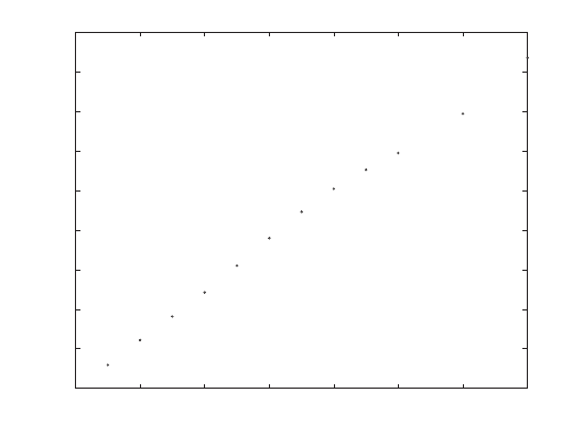
0 2 4 6 8 10 12 14
0
0.02
0.04
0.06
0.08
0.1
0.12
0.14
0.16
0.18
Detection efficiency [%]
Neutron energy [MeV]
Fig. 6.38 Fast neutron detection efficiency (%) in CH
2
as a function of the incident neutron energy
(MeV) [Gutierrez (2007)]. The detection efficiency increases with the incident neutron energy.
The differential elastic cross section is smaller for an incident neutron of 14 MeV
compared to 1 MeV as increasing neutron energy opens more inelastic channels,
then, decreasing the elastic cross section. The probability that the proton is scat-
tered at a given angle for an elastic scattering can be calculated from the differential
cross section. That probability depends on the silicon detector area and the sum of
probabilities is normalized to 1. The maximum thickness of the CH
2
converter to
be used depends on the proton range, R(θ). This thickness will change with respect
to the recoil energy, E
R
(θ), and is given by
l
max
= R(θ) cos θ. (6.158)
The incident neutrons may follow a direction either along the normal or at angle
with the normal to the converter area (Fig. 6.35) [Gutierrez (2007)] In all cases
one has to evaluate i) the probability that the proton can come out the conver-
ter into the silicon detector, depending on its range in the converter and ii) the
probability as a function of the scattering angle. One has also to account for the
increase of the collision probability with the converter thickness. Figure 6.36 shows
the detection probability of the proton as a function of the converter thickness for
neutrons incident along the normal to the converter area [Gutierrez (2007)]. The
optimal thickness of the CH
2
converter as a function of the incident neutron energy
is shown in Fig. 6.37 [Gutierrez (2007)]. The optimal thickness increases with the
incident neutron energy. For incident neutrons along the normal to the converter
area, one finds the detection efficiency as a function of the incident neutron energy
(Fig 6.38) [Gutierrez (2007)]. The results found in the figures above can be checked
with a simple calculation similar to those done for the thermal neutrons (see for
January 9, 2009 10:21 World Scientific Book - 9.75in x 6.5in ws-bo ok975x65˙n˙2nd˙Ed
Solid State Detectors 521
T
T
α
α
+
+
+
+
n n n
+
_
_
_
_
_
+
_
α
T
Silicon detector
Converter
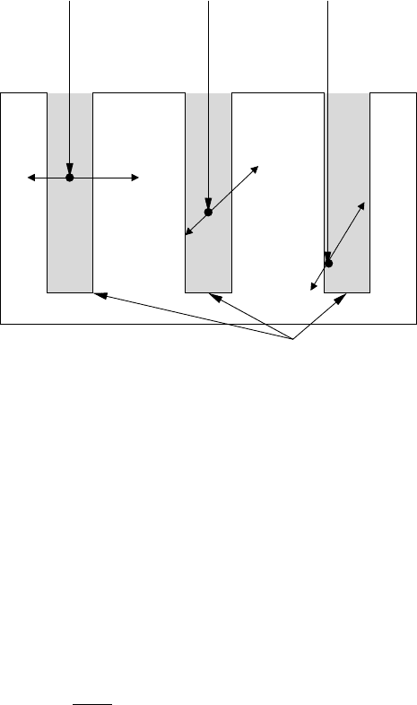
Fig. 6.39 Detection of thermal neutron detection in a detector structure with pores.
instance [Wielunski et al. (2004)]). The signal in silicon covered by a CH
2
conver-
ter is essentially given by the recoiling hydrogen, i.e., the proton. Considering the
example of 5 MeV incident neutrons, the maximum energy transfer to hydrogen
(M
n
∼ M
p
) and carbon are 5 MeV and 1.42 MeV, respectively. These values cor-
respond to a range of 347.8 µm for recoil hydrogen and 3.1 µm for recoil carbon in
polyethylene. At the same time, the elastic scattering cross section for 5 MeV inci-
dent neutrons on hydrogen and carbon are 1.63 b and 1.12 b, respectively (the cross
section values can be found in [NNDC (2008a)], for instance). The concentrations of
hydrogen and carbon in polyethylene are 7.986 ×10
22
and 3.993 ×10
22
atoms/cm
3
,
respectively. Therefore, for maximum transfer energy from fast neutrons to hydro-
gen and carbon in polyethylene, one expects:
S
N
n
P
= 0.45 × 10
−2
+ 0.14 × 10
−4
. (6.159)
The signal expected from carbon recoil is negligible compared the signal from hy-
drogen.
6.7.2 3-D Neutron Detectors
The way to improve the limited detection efficiency for neutrons of planar detectors
is to enlarge the surface between the neutron converter and the silicon detector [Uher
et al. (2007b)]. This increases the probability that the heavy charged particles will
reach the detector sensitive volume. Current semiconductor fabrication technologies
allow creation of pores into the silicon detector. The width of these pores can be
from a few micrometers up to hundreds of micrometers. The depth can be hundreds
January 9, 2009 10:21 World Scientific Book - 9.75in x 6.5in ws-bo ok975x65˙n˙2nd˙Ed
522 Principles of Radiation Interaction in Matter and Detection
of micrometers (depending on the pore width, technology and material used). These
pore dimensions are well suited for thermal neutron detectors. The principle of neu-
tron detection in a detector structure with pores is shown in Fig. 6.39. Pore depths of
200 µm or more can be fabricated by Deep Reactive Ion Etching (DRIE) [Wikipedia
(2008b)] or Electrochemical Etching (EE) [Badel (2003)] technologies. DRIE offers
a wider choice of pores sizes and shapes than EE [Uher et al. (2007b)]. On the other
hand DRIE requires expensive equipment.
6.8 Radiation Effects on Silicon Semiconductor Detectors
In this section are reviewed the general detection properties of irradiated silicon
detectors based on the standard planar (SP) and MESA technologies. The later,
less familiar nowadays, is a rather old technology introduced in 1956 [Tanenbaum
and Thomas (1956)] and has been recently revived as an alternative to standard
planar technology with the possibility to produce detectors at lower costs [Sopko,
Hazdra, Kohout, Mr´azek and Posp´ıˇsil (1997)]. The section contains a review of the
spectroscopic features of SP and MESA detectors and their behavior under parti-
cle irradiation. For the comparison, the scanning of non-irradiated and irradiated
detectors is done with heavy charged particles (e.g., α-particles and protons). Pulse-
height spectra are obtained by measuring the signal of the diodes with a standard
spectroscopy system. The study of the peaks evolution with bias voltage can provide
precise information on the active medium structure and charge collection perfor-
mances of the detector. In the case of irradiated detectors, the study of the peak
evolution with bias voltage and irradiation fluence allows the measurement of the
charge collection efficiency degradation in various regions of the diodes and structure
alteration. This section also includes a discussion of the violation of non-ionizing
energy-loss (NIEL) scaling. This scaling factor, which expresses the proportional-
ity between NIEL value and resulting damage effects, is modified for low energy
protons.
6.8.1 MESA Radiation Detectors
The MESA process for building silicon diodes has been known for a long
time [Tanenbaum and Thomas (1956)]. It has been recently revived as an alter-
native to the planar process of silicon detector production that is relatively simpler
and cheaper [Sopko, Hazdra, Kohout, Mr´azek and Posp´ıˇsil (1997)]. This relatively
inexpensive high production yield of MESA detectors combined with satisfactory
charge collection capabilities and overall performance under irradiation could favor
their choice for applications where a large number of detectors is needed such as ac-
tive medium of trackers (pixels and microstrips) or calorimeters-preshowers (pads)
for particle physics experiments. Pad and strip MESA detectors can be produced
according either to standard MESA (SM) technology or to planar MESA (PM)
January 9, 2009 10:21 World Scientific Book - 9.75in x 6.5in ws-bo ok975x65˙n˙2nd˙Ed
Solid State Detectors 523
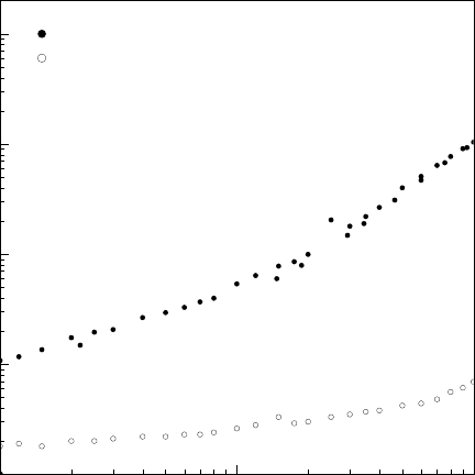
10
-2
10
-1
1
10
10
2
1 10 10
2
V (volts)
Leakage Current (µA)
Standard MESA
Planar MESA
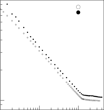
Fig. 6.40 The bulk leakage current (in µA) as a function of the applied bias voltage (in volts)
for standard MESA (SM) and planar MESA(PM) detectors, detector area of 25 mm
2
(from [Leroy
and Rancoita (2007)]).
technology. The possibility to use SM and PM silicon diodes as radiation detec-
tors has been investigated [Casse et al. (1999b); Chren et al. (2001); Houdayer et
al. (2002)]. The SM process has the disadvantage of yielding diodes that have high
surface current due to improper passivation of cut edges. The standard MESA tech-
nology has been modified in order to decrease the surface current. More generally,
one also observes much lower bulk leakage currents for planar MESA (PM) detec-
tors compared to standard MESA (SM) detectors (Fig. 6.40). After PM detectors
became available, SM detectors were no longer or rarely used. The leakage current
is larger for the SM detector (about 10 µA for a bias voltage of 100 V, detector area
of 25 mm
2
) than for the PM detector (around 50 nA for a bias voltage of 100 V,
detector area of 25 mm
2
).
This improvement observed from SM to PM results from the application of
chemical etching for producing a MESA structure with subsequent oxidation of
detector edges. As demonstrated next, the PM detectors show electrical features
comparable to those of SP detectors.
The leakage currents of the PM and SP detectors used as reference are very low
and remain low (a few nA cm
−2
for SP detectors, a few tens of nA cm
−2
for PM
detectors) with increasing applied bias voltage, even for bias voltage beyond the full
January 9, 2009 10:21 World Scientific Book - 9.75in x 6.5in ws-bo ok975x65˙n˙2nd˙Ed
524 Principles of Radiation Interaction in Matter and Detection
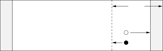
n+ p+n
Back Front
r
h
e
X
00’ w’
X
dead
w-X
dead
w0
Fig. 6.41 Schematic representation of a MESA detector with the dormant or dead layers on each
side; r represents the range of the incident particle (adapted from Nucl. Instr. and Meth. in
Phys. Res. A 460, Chren, D., Juneau, M., Kohout, Z., Lebel, C., Leroy, C., Linhart, V., Pospisil,
S., Roy, P., Saintonge, A. and Sopko, B., Study of the characteristics of silicon MESA radiation
detectors, 146–158, Copyright (2001), with p ermission from Elsevier).
depletion value.
6.8.1.1 Electrical features of Planar MESA Detectors
Several studies were done to compare the performances of planar MESA (PM) detec-
tors to standard planar (SP) detectors (these studies also involved standard MESA
(SM) detectors) [Chren et al. (2001); Houdayer et al. (2002)]. The detectors used for
these studies were typically PM detectors of average resistivity of 2 kΩ cm, 25 mm
2
area and 280 µm thickness. The SP detectors had a resistivity from 2.5 kΩ cm to
6.0 kΩ cm, an area from 25 mm
2
to 100 mm
2
, and a thickness of 300 µm. A charge
transport model has demonstrated the existence of dormant or dead layers on each
side of the MESA junctions (Fig. 6.41) [Leroy, Roy, Casse, Glaser, Grigoriev and
Lemeilleur (1999b)]. A layer of about 5 µm on each side of a PM diode is acting as a
dead or dormant layer (this layer was 14 µm deep on each side of a SM diode [Leroy,
Roy, Casse, Glaser, Grigoriev and Lemeilleur (1999b)]), consistent with charge col-
lection data. The active thickness of the MESA detector, of which a thickness X
dead
is considered dormant on each side as shown in Fig. 6.41, can be defined as
w
0
= w − 2 X
dead
.
The capacitance-versus-voltage (C −V ) curves are shown in Fig. 6.42 for a PM
detector and a SP detector of same area (25 mm
2
). The C − V curves are typical
and indicate a full depletion voltage, V
fd
, in the range of (120–150) V for both
types of detectors (PM and SP). These rather large values of V
fd
reflect the low
resistivity (2–2.5) kΩ cm of the PM and SP detectors used for the example. The
capacitance measured is larger for the PM detector compared to the SP detector
since the thickness of the PM detector, 270 µ m (280 µm corrected for the 10 µm
dead layer), is smaller than the thickness of the SP detector, of 300 µm.
The average charge collection (in fC) from the signal induced by relativistic elec-
January 9, 2009 10:21 World Scientific Book - 9.75in x 6.5in ws-bo ok975x65˙n˙2nd˙Ed
Solid State Detectors 525
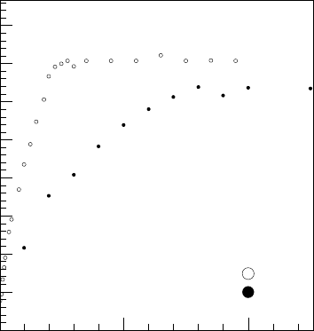
9
10
20
30
40
50
60
70
80
90
100
1 10 10
2
PM
SP
V(volts)
Capacitance (pF)
Fig. 6.42 The C − V curve features of a PM and a SP diode are compared. The full depletion
voltage, V
fd
, is found to be in the range of (120–150) V for both type of diodes (reprinted from Nucl.
Instr. and Meth. in Phys. Res. A 476, Houdayer, A., Lebel, C., Leroy, C., Roy, P., Linhart, V.,
Pospisil, S., Sopko, B., Silicon planar MESA diodes as radiation detectors, 588–595, Copyright
(2002), with permission from Elsevier).
trons from a
106
Ru source is shown in Fig. 6.43 as a function of the applied bias
voltage for a PM detector compared to that of a SP detector. Saturation is achieved
at and beyond V
fd
(value consistent with C − V measurements) for the detectors
shown in Fig. 6.43. The average charge value of ∼ 3.2 fC found at full depletion and
beyond for the PM detector is in agreement with an effective thickness of 274 µm
which is (3–4) % less than the thickness of ∼ 283 µm measured with a micrometer,
reflecting the existence of dormant or dead layers which could correspond to the
extent of the B or P diffusion zone in the PM process. The total dormant or dead
zone is larger for SM detectors (28 µm) than for PM detectors (10 µm). The average
charge value of ∼ 3.6 fC measured at full depletion and beyond for a SP detector
taken as reference for comparison is consistent with its measured (with a microm-
eter) thickness of 306 µm which is about 10% more than the thickness of the PM
detector. Note that the ratio of the average charge measured for the PM and SP de-
tectors is equal to the ratio of their thicknesses, as it should be. The resistivity of the
particular SP detector used as reference for the measurement was 5.9 kΩ cm, which
explains the smaller value of V
fd
(∼ 50 V) observed for this detector in Fig. 6.43.
January 9, 2009 10:21 World Scientific Book - 9.75in x 6.5in ws-bo ok975x65˙n˙2nd˙Ed
526 Principles of Radiation Interaction in Matter and Detection
0
0.5
1
1.5
2
2.5
3
3.5
4
100 200
SP
V (volts)
Charge (fC)
PM
Fig. 6.43 Comparison of the charge collected (in fC) as a function of the applied bias voltage (in
volts) for PM and SP detectors illuminated by electrons (mips, electron energy larger than 2 MeV
from a
106
Ru source), (reprinted from Nucl. Instr. and Meth. in Phys. Res. A 476, Houdayer,
A., Lebel, C., Leroy, C., Roy, P., Linhart, V., Pospisil, S., Sopko, B., Silicon planar MESA diodes
as radiation detectors, 588–595, Copyright (2002), with permission from Elsevier).
6.8.1.2 Spectroscopic Characteristics of MESA Detectors
The spectroscopic technique has been applied to the study of PM detectors [Chren et
al. (2001); Houdayer et al. (2002)]. Alpha sources (
239
Pu,
241
Am,
244
Cm) were used
to perform spectroscopic measurements with α-particles in vacuum. The spectra
obtained with
239
Pu (α-particle energy of 5.157 MeV),
241
Am (α-particle energy of
5.486 MeV), and
244
Cm (α-particle energy of 5.805 MeV) are shown in Fig. 6.44 for
α-particles incident on the front and back sides of a PM detector for two shaping
times of 0.25 µs [Fig. 6.44(a)–(c)] and 1.0 µs [Fig. 6.44(d)–(f)]. The comparison of
the peaks evolution with voltage for the PM and a silicon surface barrier detector
(SSBD) of reference allows the determination of the CCE.
Shifts among peaks and their splitting are caused by different energy losses of
particles entering through non-sensitive layers close to or on the detector surface. As
already emphasized in the section on standard planar detectors, the capability to
measure shifts at the level of a keV is equivalent to measuring layer thicknesses
of about ten nanometers. Therefore, an investigation of the detector fine-structure
becomes possible [Chren et al. (2001)] as illustrated in Fig. 6.45.
January 9, 2009 10:21 World Scientific Book - 9.75in x 6.5in ws-bo ok975x65˙n˙2nd˙Ed
Solid State Detectors 527
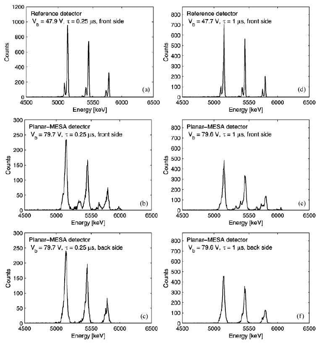
Fig. 6.44 Spectra representing the response of a PM detector to α-particles from Pu, Am, and Cm
sources incident on the front side [(b) and (e) for shaping time
τ
of 0.25 and 1.0
µ
s, respectively] and
back side [(c) and (f) for shaping time τ of 0.25 and 1.0 µs, respectively] of the detector, compared
to the response [(a) and (d) for shaping time τ of 0.25 and 1.0 µs, respectively] of a silicon surface
barrier detector (SSBD) used as reference. The applied reverse bias voltage was ∼ 48 and 80 V for
the SSBD and PM detectors, respectively. The fine structure of alpha spectra is clearly resolved
by the SSBD. The influence of PM detector electrode structure is explained in Fig. 6.45. The peak
positions are determined with a precision better than 5 keV (reprinted from Nucl. Instr. and
Meth. in Phys. Res. A 460, Chren, D., Juneau, M., Kohout, Z., Lebel, C., Leroy, C., Linhart,
V., Pospisil, S., Roy, P., Saintonge, A. and Sopko, B, Study of the characteristics of silicon MESA
radiation detectors, 146–158, Copyright (2001), with permission from Elsevier).
6.8.2 Results of Irradiation Tests of Planar MESA Detectors
The characteristics of MESA detectors as a function of fluence were investigated
in view of their possible use in high particle fluence environment. The irradiation
studies of PM detectors have really been limited up to now to one experiment where
January 9, 2009 10:21 World Scientific Book - 9.75in x 6.5in ws-bo ok975x65˙n˙2nd˙Ed
528 Principles of Radiation Interaction in Matter and Detection
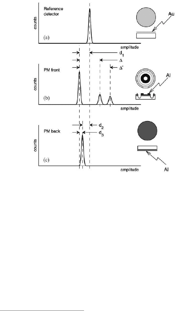
Fig. 6.45 Illustration of the sensitivity of the spectroscopic method applied to PM detectors. The
response of a SSBD used as reference (a) is compared to the response of a PM detector illuminated
by α-particles (b) on the front side and (c) on the back side. Shifts among p eaks and their splitting
are caused by different energy-losses of particles entering through non-sensitive layers close to or
on the detector surface. d
1
is the difference of front side electrode structure thickness between the
reference detector (Au + p − n junction) and the PM detector (Al + p − n junction) expressed
in energy losses; d
2
is the difference of thickness expressed in energy losses in front side reference
detector structure (Au + p − n) and back side PM detector (Al + n
+
n). d
3
is the difference
expressed in energy losses in front side PM detector structure (Al + p − n) thickness and back
side PM detector structure (Al + n
+
− n) thickness. Also defined are ∆: the energy loss in front
side Al of PM detector, and ∆
0
: the energy loss in front side SiO
2
layer in MESA valley of PM
detector (reprinted from Nucl. Instr. and Meth. in Phys. Res. A 460, Chren, D., Juneau, M.,
Kohout, Z., Lebel, C., Leroy, C., Linhart, V., Pospisil, S., Roy, P., Saintonge, A. and Sopko, B,
Study of the characteristics of silicon MESA radiation detectors, 146–158, Copyright (2001), with
permission from Elsevier).
a set of PM diodes (25 mm
2
area, ∼ 280 µm thickness and ∼ 2 kΩ cm resistivity)
were exposed to low energy (10 MeV) protons (hardness factor
∗
: theoretical is κ ∼
4.5, measured is ∼ 2.2) [Bechevet, Glaser, Houdayer, Lebel, Leroy, Moll and Roy
(2002)]. The effective doping concentration (N
eff
) of a semiconductor diode can be
extracted from measurement of the capacitance (C) as a function of the applied
∗
The reader can see Sect. 4.1.3 (and references therein) for an general treatment of the hardness
factor.

January 9, 2009 10:21 World Scientific Book - 9.75in x 6.5in ws-bo ok975x65˙n˙2nd˙Ed
Solid State Detectors 529
Table 6.4 Range of protons in silicon as a function
of energy (from [Leroy and Rancoita (2007)]). The
ranges were calculated as a function of the proton
energy using the SRIM code, which employs Ziegler’s
stopping tables [Ziegler, Biersack and Littmark
(1985a)]
Energy (MeV) 7 8 9 10
Range (µm) 380 476 584 700
bias (V ) (see Sect. 6.1.3).
The effective doping concentration (N
eff
) as a function of fluence (Φ) is given
by Eq. (6.75) [Pitzl et al. (1992)]. The values of the parameters of the irradiated
PM and SP diodes extracted by fitting Eq. (6.75) to the experimental data (N
eff
as a function of proton fluence) show that the parameter b is not affected by the
MESA process [Bechevet, Glaser, Houdayer, Lebel, Leroy, Moll and Roy (2002)],
while the parameter c could be affected since its value should be smaller [Dezillie et
al. (1999)], reflecting the higher initial donor concentration (N
d
) of the PM diodes
compared to the SP diodes.
It is a standard procedure to heat the detectors at 80 C for up to 17 hours to
simulate their ageing during the 10 years of operation of the LHC experiments. The
irradiation induced change in the effective doping concentration (∆N
eff
) as a func-
tion of the heating time (t) is given by [Lindstroem, Moll and Fretwurst (1999)]:
∆N
eff
(t) = N
A
exp(−t/τ
a
) + N
C
+ N
Y
µ
1 −
1
1 + t/τ
Y
¶
, (6.160)
where N
A
and τ
a
are the short-term annealing constants; N
C
represents the so-called
stable damage constant, which consists of an “incomplete donor removal” and the
introduction of negative space-charge proportional to fluence; finally, N
Y
and τ
Y
are the long-term reverse annealing constants. From results reported in [Bechevet,
Glaser, Houdayer, Lebel, Leroy, Moll and Roy (2002)] it is observed that before
“inversion”
†
(Φ < 10
13
p cm
−2
) the short term annealing (N
A
) is about 3 times
more in amplitude for SP than for the PM detectors, while after inversion (Φ >
10
13
cm
−2
), the difference is about a factor 2. The anti-annealing parameter, N
Y
,
for PM and SP detectors is comparable before inversion but N
Y
is about 25 % larger
for the PM detectors after inversion.
The leakage current was recorded (guard ring connected) during the measure-
ments of the capacitance (C) as a function of the applied voltage (V ). These
measurements were performed at room temperature with the leakage current
†
The reader can also see the discussion in Sects. 4.3.5 and 4.3.6 about the experimental obser-
vation that, at large particle fluences, the Hall coefficient changes sign in n-type substrate with
high-resistivity (before irradiation).