Martienssen W., Warlimont H. (Eds.). Handbook of Condensed Matter and Materials Data
Подождите немного. Документ загружается.

622 Part 4 Functional Materials
Table 4.1-56 Melting point T
m
of gallium compounds
Crystal Melting point T
m
(K) Remarks
Gallium nitride GaN 2791 GaN sublimes without decomposition around 800
◦
C
Gallium phosphide GaP 1749
Gallium arsenide GaAs 1511
Gallium antimonide GaSb 991 (1)
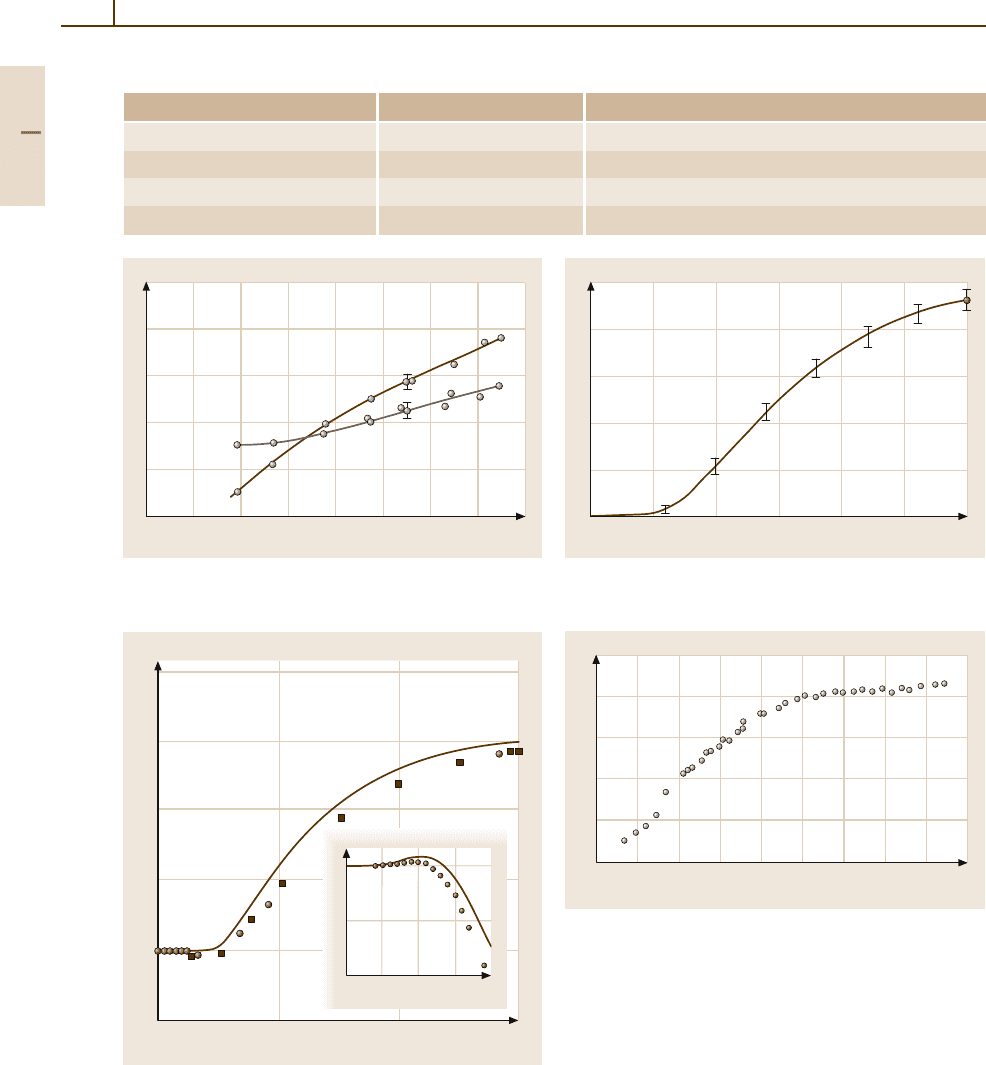
1
2
7
6
5
4
3
2
0 100 200 300 400 500
T (K)
α (10
–6
K
–1
)
600 700 800
GaN
Fig. 4.1-78 GaN. Coefficient of linear thermal expansion
vs. temperature (curve 1, α
⊥
; curve 2, α
) [1.75]
α (10
–6
K
–1
)
8
100
300
T (K)
6
2
–2
2000
0
GaAs
T(K)
0
–3
–6
0 5 10 15 20
∆
α (10
–8
K
–1
)
Fig. 4.1-80 GaAs. Coefficient of linear thermal expansion.
Experimental data points, and curves from an ab initio
pseudopotential calculation [1.77]
5
4
3
2
1
0
0 50 100 150 200 250 300
T (K)
GaP
α (10
–6
K
–1
)
Fig. 4.1-79 GaP. Linear thermal expansion coefficient vs.
temperature between 0 K and 300 K [1.76]
8
6
4
2
0
–2
0 40 80 120 160 200 240 280 320 360
T (K)
α (10
–6
K
–1
)
GaSb
Fig. 4.1-81 GaSb. Linear thermal expansion coefficient vs.
temperature measured with a quartz dilatometer. High-
temperature range [1.56,57]
Part 4 1.2
Semiconductors 1.2 III–V Compounds 623
Table 4.1-57 Linear thermal expansion coefficient α of gallium compounds
Crystal Expansion coefficient α Remarks Temperature dependence
(10
−6
K
−1
)
Gallium nitride GaN α
parall
5.59 X-ray diffraction Fig. 4.1-78
α
perpend
3.17
Gallium phosphide GaP 4.65 300 K Fig. 4.1-79
Gallium arsenide GaAs 5.87 300 K Fig. 4.1-80
Gallium antimonide GaSb 7.75 (50) Around 300 K; X-ray diffraction Fig. 4.1-81
Table 4.1-58 Heat capacity c
p
and Debye temperature Θ
D
of gallium compounds
Crystal Heat capacity (J/mol K) Temperature (K) Debye temperature (K) Remarks
Gallium nitride GaN 600 Estimated
Gallium phosphide GaP 49.65 800 445
Gallium arsenide GaAs 46.90 300 344
Gallium antimonide GaSb 266
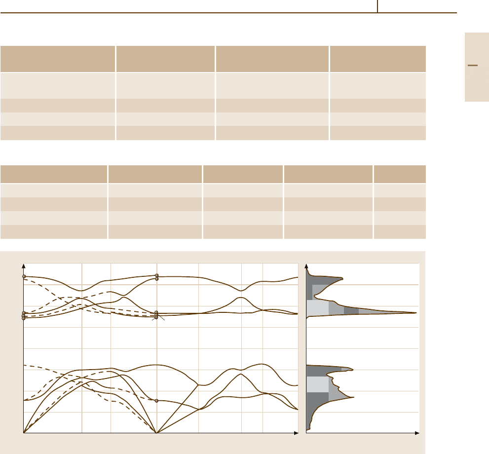
800
700
600
500
400
300
200
100
0
ΓΓ
Wavenumber ν
–
(cm
–1
)
Wave vector q
KM A HL A
DOS
GaN
E
1
(LO)
A
1
(TO)
E
1
(LO)
A
1
(TO)
A
1
(LO)
E
1
(TO)
B
1
E
2
B
1
E
2
B
1
E
2
B
1
E
2
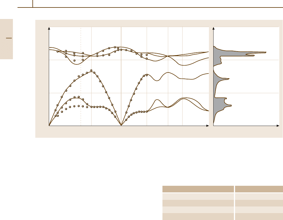
Fig. 4.1-82 GaN (wurtzite structure). Phonon dispersion curves (decomposed according to different irreducible represen-
tations along the main symmetry directions) and density of states, from a model-potential calculation. The circles show
Raman data from [1.78]. From [1.79]
Part 4 1.2
624 Part 4 Functional Materials
Table 4.1-59 Phonon wavenumbers of gallium compounds. Gallium nitride (GaN), T = 300 K, from Raman spec-
troscopy; gallium phosphide (GaP), RT, from an analysis of Raman, neutron, luminescence, and absorption data; gallium
arsenide (GaAs), T = 296 K, from coherent inelastic neutron scattering; gallium antimonide (GaSb), T = 300 K, from
second-order Raman effect
GaN GaP
Symmetry
Branch Wavenumber Symmetry Branch Frequency
point
(cm
−1
) point (THz)
˜
ν
low
(E
2
) 145 ν(Γ) TO 10.95 (1)
˜
ν (A
1
) TO 533 LO 12.06 (1)
˜
ν (E
1
) TO 560 ν (X) TA 3.13 (3)
˜
ν
high
(E
2
) 567 LA 7.46 (6)
˜
ν (A
1
) LO 735 TO 10.58 (3)
˜
ν (E
1
) LO 742 LO 11.09 (6)
ν (L) TA 2.58 (3)
LA 6.45 (3)
TO 10.64 (3)
LO 11.24 (3)
GaAs GaSb
Symmetry
Branch Frequency Symmetry Branch Wavenumber
point (THz) point (cm
−1
)
ν(Γ
15
) LO 8.55 (20)
˜
ν (L)
TA 46
TO 8.02 (8)
˜
ν (X)
TA 56
ν (X
1
) TA 2.36 (2)
˜
ν (W)
TA 75
LO 7.22 (15)
˜
ν (L)
LA 155
ν (X
3
) LA 6.80 (6) LO 204
ν (X
5
) TO 7.56 (8)
˜
ν (X)
LO 210
ν (L
1
) LA 6.26 (10)
˜
ν (L, X, Σ)
TO 218
LO 7.15 (7)
ν (L
3
) TA 1.86 (2)
TO 7.84 (12)
Table 4.1-60 Phonon dispersion curves of gallium com-
pounds
Crystal Figure
Gallium nitride GaN Fig. 4.1-82
Gallium phosphide GaP Fig. 4.1-83
Gallium arsenide GaAs Fig. 4.1-84
Gallium antimonide GaSb Fig. 4.1-85
Part 4 1.2
Semiconductors 1.2 III–V Compounds 625
400
300
200
100
0
ΓΓ
Wavenumber ν
–
(cm
–1
)
Wave vector q
KX L X W L
DOS
GaP
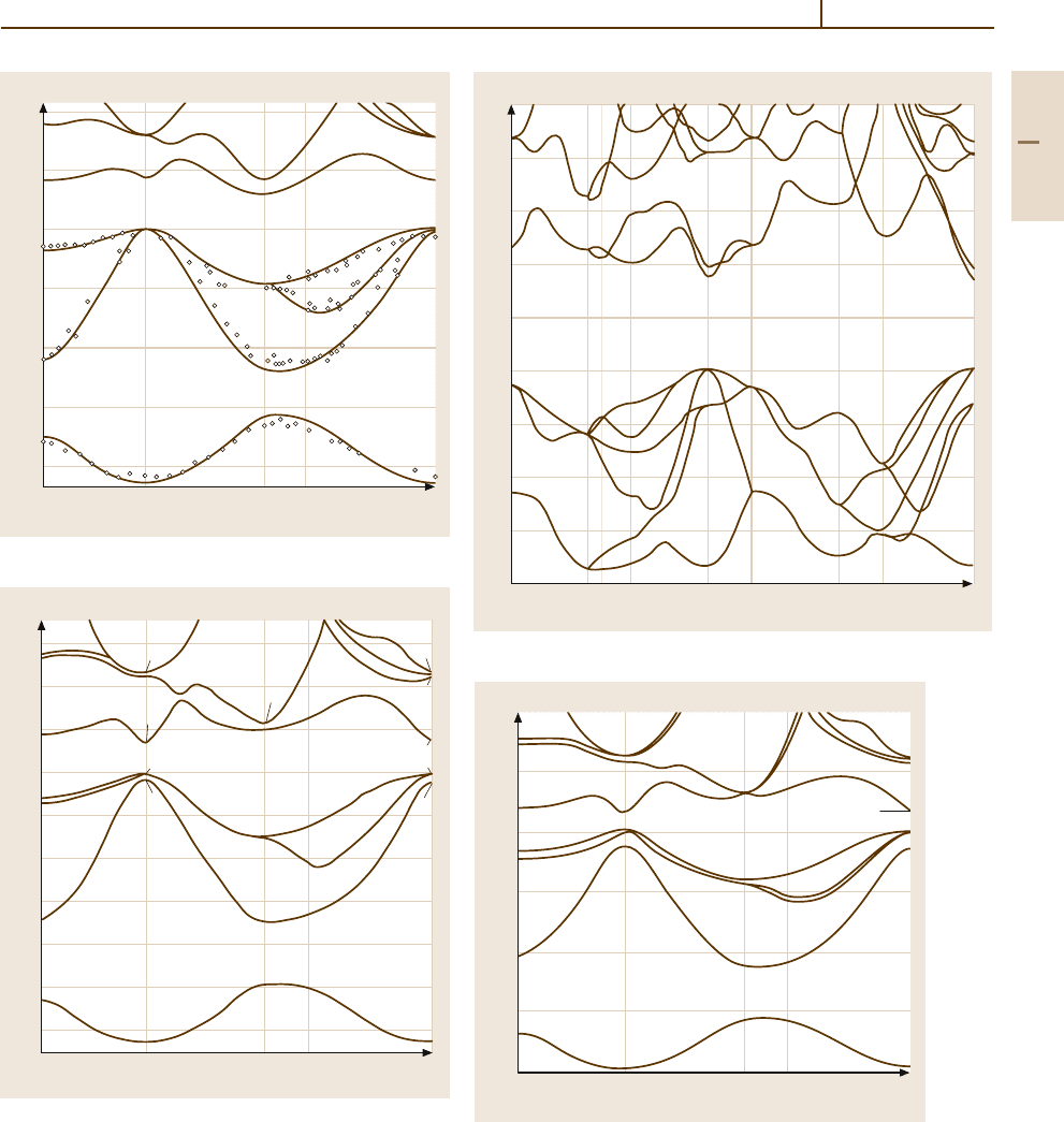
Fig. 4.1-83 GaP. Phonon dispersion curves (left panel) and density of states (right panel). Experimental data points
from [1.80] (open symbols) and from [1.81] (filled symbols) and theoretical curves from ab initio calculations [1.82].
From [1.82]
400
300
200
100
0
ΓΓKX L X W L
Wavenumber ν
–
(cm
–1
)
Wave vector q
DOS
GaAs
Fig. 4.1-84 GaAs. Phonon dispersion curves (left panel) and phonon density of states (right panel) [1.16]. Experimental
data points [1.83] and ab initio calculations [1.16].
Part 4 1.2
626 Part 4 Functional Materials
ΓΓ
300
200
100
0
Wavenumber ν
–
(cm
–1
)
Wave vector q
KX L X W L
DOS
GaSb
Fig. 4.1-85 GaSb. Phonon dispersion curves (left panel) and phonon density of states (right panel) [1.16]. Experimental
data points [1.84] and ab initio calculations [1.16]
B. Electronic Properties
Tables 4.1-61 – 4.1-66.
Band Structures of Gallium Compounds. Gallium Ni-
tride (GaN). The band structure is shown in Fig. 4.1-87.
Owing to spin–orbit interaction, the two top valence
bands (Γ
6
and Γ
1
) are split into three spin-degenerate
bands, one with quantum number J
z
= 3/2(Γ
9
) and
two with Jz = 1/2(Γ
7
)’. For convenience, the notation
A, B, C is used for these bands.
Gallium Phosphide (GaP). Gallium phosphide is an
indirect-gap semiconductor. The lowest set of conduc-
tion bands shows a camel’s back structure; the band
minima are located on the ∆ axes near the zone
boundary. The valence bands show the usual structure
characteristic of zinc blende semiconductors.
The spin–orbit splitting of the top of the valence
band is negligible compared with most other energy
separations in the band structure. Therefore, Fig. 4.1-86
shows the band structure calculated without inclusion of
spin–orbit splitting; the symmetry symbols of the high-
symmetry band states are symbols of the single group
of the zinc blende structure.
Gallium Arsenide (GaAs). Gallium arsenide is a direct-
gap semiconductor. The minimum of the lowest
Table 4.1-61 First Brillouin zones of gallium compounds
Crystal Figure
Gallium nitride GaN Fig. 4.1-24
Gallium phosphide GaP Fig. 4.1-23
Gallium arsenide GaAs Fig. 4.1-23
Gallium antimonide GaSb Fig. 4.1-23
conduction band is located at Γ; higher sets of min-
ima at L and near X (about 10% away from the zone
boundary) are also important for the optical and trans-
port properties. The minimum near X most probably
has a camel’s back-like structure similar to that of GaP,
AlAs, and AlSb. The valence bands have the usual struc-
ture characteristic of zinc blende crystals (Fig. 4.1-88).
Gallium Antimonide (GaSb). The conduction band of
GaSb is characterized by two types of minima, the lowest
minimum at Γ and slightly higher minima at the L points
at the surface of the Brillouin zone. A third set of minima
at the X points has been detected in optical experiments.
The valence bands show the usual structure common to
zinc blende semiconductors (Fig. 4.1-89).
Part 4 1.2
Semiconductors 1.2 III–V Compounds 627
E (eV)
6
3
0
–3
–6
–9
–12
Wave vector k
XΓ U,K ΓL Λ∆ Σ
GaP
L
3
L
1
L
1
L
3
L
2
Γ
1
Γ
15
Γ
1
Γ
15
Γ
15
Γ
15
Γ
1
Γ
1
K
1
K
1
K
1
K
1
K
1
K
2
X
3
X
1
X
5
X
3
X
1
Fig. 4.1-86 Band structure of gallium phosphide
6
4
2
0
–2
–4
–6
–8
–10
–12
U,KXL ΓΓΣΛ∆
E (eV)
Wave vector k
L
6
Γ
6
Γ
6
X
6
GaAs
L
6
X
6
L
6
X
6
Γ
7
Γ
7
L
4,5
X
7
Γ
8
Γ
8
L
6
Γ
6
Γ
6
X
6
L
6
Γ
7
Γ
7
X
7
L
4,5
Γ
8
Γ
8
Fig. 4.1-88 Band structure of gallium arsenide
10
8
6
4
2
0
–2
–4
–6
–8
ΓΣRL TAASHPKUM ∆Γ
E (eV)
Wave vector k
GaN
1
2
3
5
6
1,3
5,6
3
3
3
3
3
3
3
3
1
1
1
1
1
3
3
2
1
5
4
1,3
1,3
1,3
1,3
1,3
2
1
4
6
2,4
1,2
1,2
5,6
Fig. 4.1-87 Band structure of gallium nitride
E (eV)
6
3
0
–3
–6
–9
–12
Wave vector k
XΓ U,K ΓL Λ∆ Σ
L
6
L
4,5
L
6
L
4,5
L
6
L
6
L
6
Γ
6
Γ
7
Γ
8
Γ
6
Γ
7
Γ
8
Γ
8
L
6
Γ
7
Γ
7
Γ
8
X
7
X
6
X
6
X
6
X
6
X
7
GaSb
L
6
Fig. 4.1-89 Band structure of gallium antimonide
Part 4 1.2
628 Part 4 Functional Materials
Table 4.1-62 Energy gaps of gallium compounds
Crystal Quantity Bands Energy (eV) Temperature (K) Remarks
Gallium nitride GaN E
g, dir
3.503 (2) 1.6 Photoluminescence
A exciton 3.4751 (5) Transition from Γ
9v
B exciton 3.4815 (10) Transition from upper Γ
7v
C exciton 3.493 (5) Transition from lower Γ
7v
Gallium phosphide GaP E
g, ind
Γ
8v
to ∆
5c
2.350 (1) 0 Extrapolated, from exciton data
2.272 300
E
g, ind
Γ
15v
to L
1c
2.637 (10) 78 Electroabsorption
Gallium arsenide GaAs E
g, dir
Γ
8v
to Γ
6c
1.51914 0 Extrapolated, photoluminescence
1.424 (1) 300 Differentiated reflectivity
E
g, th
1.604 0 Extrapolated,
intrinsic carrier concentration
Gallium antimonide GaSb E
g, dir
Γ
8v
to Γ
6c
0.822 0 Extrapolated, electroreflectance
0.75 300
Table 4.1-63 Exciton binding energies of gallium compounds
Crystal Quantity Energy (meV) Remarks
Gallium nitride GaN E
A
b
20 A exciton, photoreflectance
E
B
b
18.5 B exciton, photoreflectance
E
C
b
22.4 C exciton, photoluminescence
Gallium antimonide GaSb E
b
1.6 Calculated ground-state binding energy
Table 4.1-64 Spin–orbit splitting energies of gallium compounds
Crystal Quantity Bands Energy Temperature Remarks
(meV) (K)
Gallium nitride GaN ∆
1
9.8 Epitaxial films,
∆
2
5.6 reflectance measurements
∆
3
5.6
Gallium phosphide GaP ∆
0
Γ
8v
to Γ
7v
80 (3) 100–200 Splitting of Γ
15v
into Γ
8v
(upper level) and
Γ
7v
(lower level)
Gallium arsenide GaAs ∆
0
Γ
15v
346.4 (5) 1.7 Splitting of Γ
15v
valence band state into Γ
7v
and Γ
8v
, magnetoabsorption splitting of Γ
15
conduction band state into Γ
7c
and Γ
8c
,
∆
0
Γ
15c
171 (15) 4.2 electroreflectance
Gallium antimonide GaSb ∆
0
Γ
8v
to Γ
7v
756 (15) 10 Electroreflectance
∆
0
Γ
7c
to Γ
8c
213 (10)
∆
1
L
4,5v
to L
6v
430 (10)
∆
1
L
4,5c
to L
6c
130
Part 4 1.2
Semiconductors 1.2 III–V Compounds 629
Table 4.1-65 Effective masses of electrons (m
n
) and holes (m
p
) for gallium compounds (in units of the electron mass m
0
)
GaN GaP
m
n
0.22 6K Cyclotron resonance, m
n, parall
Near ∆
min
7.25 1–20K At bottom of camel’s back
polaron mass
m
n, parall
0.20 (6) From reflectance m
n, perp
Near ∆
min
0.21 Luminescence
spectrum
m
n, perp
0.20 (2) m
n, parall
Away 2.2 High above bottom of
from ∆
min
camel’s back
m
(A)
p
1.01 7K Estimated from m
p, heavy
Parallel 0.67 (4) 1.6 Cyclotron resonance
binding energies to [111] at 1.6K
m
(B)
p
1.1 m
p, light
Parallel 0.17 (1) Parallel
to [111] to [111]
m
(C)
p
1.6 m
p, so
0.4649 0 Spin–orbit mass,
calculated from k · p model
GaAs
m
n
(Γ) 0.0662 (2) 1.6 Cyclotron resonance
m
p, heavy
Parallel to [100] 0.34 10 K Electronic Raman scattering
Parallel to [111] 0.75
m
p, light
Parallel to [100] 0.094
Parallel to [111] 0.082
GaSb
m
n
(Γ) 0.039 (5) 2K Optically detected cyclotron resonance
m
n
(L
6c
) 0.11 Transverse mass
0.95 Longitudinal mass
0.226 Density-of-states mass
m
p, heavy
0.29 (9) 30 K B parallel to [100] Stress-modulated magnetoreflectance
0.36 (13) B parallel to [110]
0.40 (16) B parallel to [111]
m
p, light
0.042 (2)
Table 4.1-66 Electron g-factor g
c
of gallium antimonide
Crystal g
c
Temperature (K) Remarks
Gallium antimonide GaSb −9.1 (2) 4.2–50 Magnetoluminescence
C. Transport Properties
Tables 4.1-67 and 4.1-68.
Electronic Transport, General Description. Gallium
Nitride (GaN). Undoped GaN is normally an n-type
conductor. Carrier concentrations in undoped films
can vary from 5 ×10
19
cm
−3
to 5×10
16
cm
−3
because
of unintentional incorporation of extrinsic impurities,
mainly silicon and oxygen. In the purest α-GaN ma-
terial (n = 10
17
cm
−3
), conductivities of the order of
10 Ω cm have been found at 300 K. For the tem-
perature dependence of the electrical resistivity, see
Fig. 4.1-90.
Gallium Phosphide (GaP). Even in high-puritysamples,
intrinsic conduction occurs in gallium phosphide only
above 500
◦
C. Thus, the transport properties are in gen-
eral determined by the properties of impurities and
lattice defects. The data for the electrical conductivity σ
of pure n-type material are found to lie around 0.5 Ω cm
at 300 K.
Part 4 1.2
630 Part 4 Functional Materials
As in the case of GaAs, semi-insulating GaP can be
obtained by doping with shallow donors and acceptors
and with deep centers. Resistivities at room temperature
are of the order of 10
8
–10
11
Ω cm. Typical data at high
temperatures are shown in Fig. 4.1-91.
Gallium Arsenide (GaAs). At low fields, the electrons
are in the Γ
6
minima at the zone center. The domi-
nating scattering process at room temperature is polar
optical scattering, while below 60 K the most important
contribution to the lattice mobility is from piezoelectric
potential scattering. At room temperature, the hole mo-
bility of samples with p < 5×10
15
cm
−3
is governed by
lattice scattering alone. An intrinsic carrier concentra-
tion of n
i
= 2.1×10
6
cm
−3
has been found at T =300 K
(Fig. 4.1-92).
Owing to the very low intrinsic carrier concentration,
the electrical conductivity of GaAs at 300 K is deter-
1
10
–1
10
–2
10
–3
6
4
8
2
2
6
4
8
6
4
8
2
0 20406080100120
100 30 20 15 1050
T
–1
(10
–3
Κ
–1
)
ρ (Ω cm)
1
GaN
2
3
4
5
6
7
8
T (K)
Fig. 4.1-90 GaN. Resistivity of several undoped samples
(1 – 7) and a Zn-doped sample (8) vs. reciprocal tempera-
ture [1.85]
mined by charge carriers provided by impurities. Only
under certain doping conditions (e.g. compensation of
shallow acceptor levels by donor impurities and over-
compensation by deep Cr levels) can the Fermi level
be pinned in the middle of the energy gap and nearly
intrinsic conduction achieved (semi-insulating GaAs,
ρ =10
5
–10
9
Ω cm).
Gallium Antimonide (GaSb). Transport in n-type GaSb
is complicated by the contribution of three sets of con-
duction bands with minima located at Γ,L,andX.The
data on transport coefficients can be consistently ex-
plained by a three-band model, the X bands contributing
to transport above 180
◦
C. Intrinsic carrier concentra-
tions n
i
of the order of 10
14
cm
−3
have been estimated
for a temperature T = 365 K.
In p-type GaSb, a multiellipsoidal model has to be
used at low temperatures, taking into account the shift
of the heavy- and light-hole bands away from k = 0.
At high temperatures, a warped-sphere model (as in the
case of Si and Ge) is adequate.
10
12
10
11
10
10
10
9
10
8
10
7
10
6
10
7
10
6
10
5
10
4
10
3
10
2
10
10
3
10
2
10
1.0 2.01.5 2.5
T
–1
(10
–3
K
–1
)
n/T
3/2
(cm
–3
/K
3/2
)
µ
H, n
(cm
2
/V s)
ρ (Ω cm)
GaP
n/T
3/2
ρ
µ
H, n
Fig. 4.1-91 GaP. Resistivity, Hall mobility, and electron
concentration (divided by T
−3/2
) vs. temperature for
a semi-insulating sample [1.86]
Part 4 1.2
Semiconductors 1.2 III–V Compounds 631
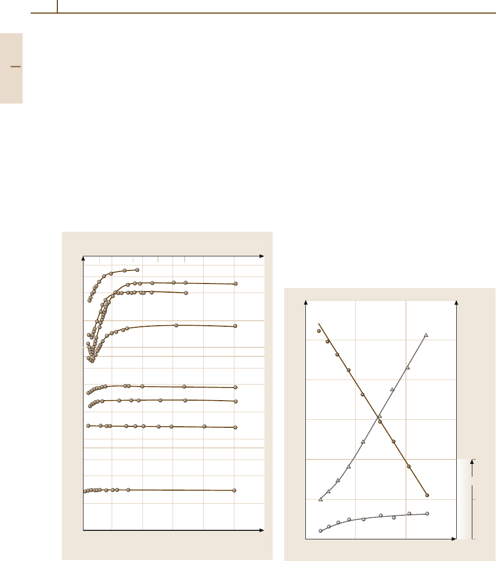
Table 4.1-67 Electron and hole mobilities µ
n
and µ
p
of gallium compounds
Crystal Temperature Carrier concentration µ
n
µ
p
Remarks
(K) (cm
−3
) (cm
2
/Vs) (cm
2
/Vs)
Gallium nitride 300 n = 3×10
16
900 Hall mobility
a
p =5×10
13
350 β-GaN, Hall mobility
Gallium phosphide RT 160 135 Thin films, Hall mobility,
maximum mobility
b
Gallium arsenide 300 2400–3300 Bulk GaAs, Hall mobility
c
300 400 Hall mobility
Gallium antimonide 300 n = 1.2×10
16
7620 MBE-grown on GaSb substrates
300 680 Hall mobility
a
See Fig. 4.1-93 for the temperature dependence of the electron mobility in GaN.
b
See Figs. 4.1-94a,b for the temperature dependence of the electron and hole mobilities in GaP.
c
See Figs. 4.1-95 and 4.1-96 for the temperature dependences of the electron and hole mobilities in GaAs.
T
–1
(10
–4
K
–1
)
n
i
(cm
–3
)
T (K)
10
19
8
6
4
2
10
17
10
16
10
15
10
14
10
13
10
12
10
11
10
10
10
9
10
8
10
7
10
6
10
5
10
4
10
18
8
6
4
2
10
17
8
6
4
2
10
16
8
6
4
2
10
15
n
i
(cm
–3
)
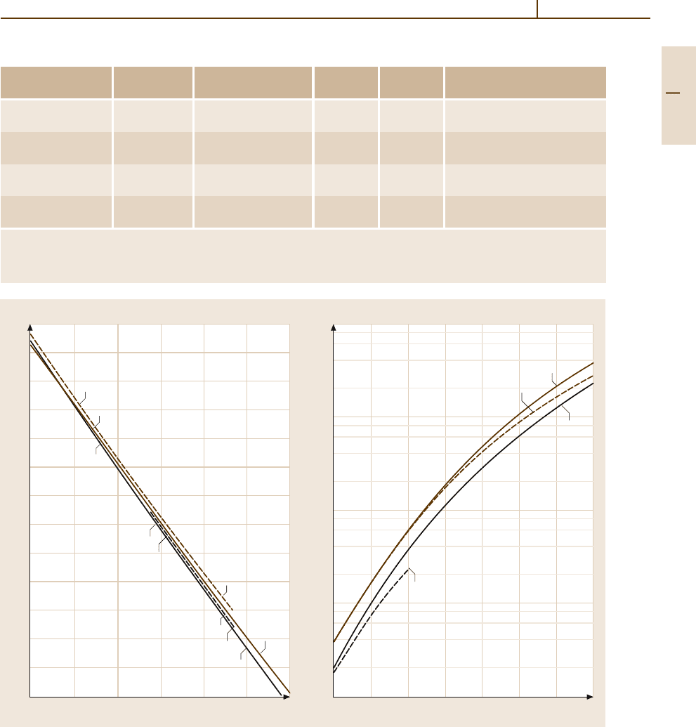
10 15 20 25 30 35 40 800 900 1000 1100 1200 1300 1400 1500
GaAs
D
B
A
G
L
D
G
F
A
B
B
D
A
C
Fig. 4.1-92 GaAs. Intrinsic carrier concentration vs. reciprocal temperature for the range 250–1000 K and vs. temperature
for the range 800–1500 K. The solid curves (A) are the result of a critical discussion of the literature data. The other
curves (B – G) represent data from other sources [1.87]
Part 4 1.2