Zuo-Guang. Ye Advanced Dielectric Piezoelectric and Ferroelectric Materials: Synthesis, Characterisation and Applications
Подождите немного. Документ загружается.

Handbook of dielectric, piezoelectric and ferroelectric materials540
WPNL2204

541
18.1 Introduction
The principal thrust of ferroelectric thin-film research and development has
been to the production of non-volatile random access memories (FRAMs);
in contrast to ‘volatile’ dynamic RAMs (DRAMs), such non-volatile devices
retain stored memory in the event of a power failure. Although DRAMs are
volatile, they are unlikely to disappear in the foreseeable future, because
they combine high density (Gbits), high speed and low cost. Nevertheless, in
applications where volatility would require heavy, power-consuming and
cumbersome hard-disk back-up memory (banking, aerospace, or mobile
telephones and digital cameras), the new ferroelectric FRAMs compete
primarily with ‘Flash’/EEPROM devices (electrically erasable read-only
memories). The long-term advantages of FRAMs over EEPROMs are in part
due to the lowering of standard silicon logic levels from the present 5.0 volt
standard to 3.3V, 1.1V and eventually 0.5V. FRAMs can already meet these
lower voltage requirements, whereas it will be physically difficult for Flash
devices to do so, perhaps necessitating cumbersome and unreliable ‘charge
pumps’ to provide 5V internally from a 1.0V external source. The next
application of FRAMs is likely to be memories in digital cameras, and the
size (see below) is now nearly sufficient for use as the audio memory in
stereo devices such as the Sony Walkman. FRAMs are already in use for
‘smart’ credit cards and for video games (a 32 kb FRAM from Fujitsu is
already in every Sony Playstation 2).
Despite the attention focused on FRAMs, memories are not the only
trendy development in ferroelectric thin-film devices (Clark and Lagerwall
1980; Lagerwall 2004), and below I review a dozen other major trends and
areas of R&D, based in part upon my recent reviews of the field in Science
and the Journal of Physics Condensed Matter (Scott, 2006ab).
Recent prototype applications and milestones include ultra-fast (280 ps)
switching (Li et al., 2004), cheap room-temperature magnetic field detectors
to replace SQUIDs (superconducting quantum interference devices),
18
Ferroelectric nanostructures for
device applications
J F SCOTT, Cambridge University, UK
WPNL2204
Handbook of dielectric, piezoelectric and ferroelectric materials542
piezoelectric nanotubes for microfluidic systems, electrocaloric coolers for
computers, phased-array radar and three-dimensional trenched capacitors
for DRAMs. Tera-bit/square-inch ferroelectric arrays of lead zirconate–titanate
have been reported on Pt nanowire interconnects, and nano-rings with 5–10
nm diameters. Finally, electron emission from ferroelectrics is a relatively
unexploited phenomenon that already yields prototypes of cheap, very small,
high-power microwave devices, as well as miniature X-ray and neutron
sources (‘cold fusion’).
18.2 Ferroelectric nanostructures
The prefix ‘nano-’ is generally defined as <0.1 micrometres, and although
ferroelectric capacitors and related devices are now submicrometre, they are
400–500nm on a side, not 100, with thickness ca. 50–150nm (Fig. 18.1). As
the sizes of ferroelectric cells continue to shrink to true nano-scale, two
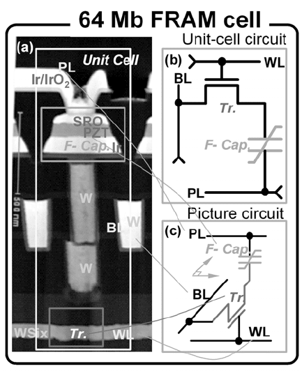
18.1
(a) TEM cross-section for state-of-the-art FRAM: a 64 Mb PZT
device with cell size approximately 400 × 450 × 144 nm
3
. (b) and (c)
illustrate the relationship of each component in the TEM micrograph
to the equivalent circuit diagram. The symbols on the left side are: Ir
– iridium; SR – SrRuO
3
; W – tungsten; and Tr. – transistor. On the
right side: WL – word-line; BL – bit-line; PL – plate; Tr. – transistor;
and F – ferroelectric thin film.” (Samsung; used by permission).
WPNL2204
Ferroelectric nanostructures for device applications 543
physics questions are important for nano-ferroelectrics: first, are there physical
phenomena such as crystallographic phases or domain structures that are
stable at these sizes that are not present in bulk? And second, are the device
properties qualitatively different on the nano-scale? Phenomena one might
examine include ferroelectric quantum dots and confinement energies, direct
electron tunnelling, unusual phases due to substrate interface strain, and the
general properties of semiconducting ferroelectrics. Most textbooks make
the assumption that ferroelectrics are insulators. Although this is a good
approximation for bulk samples (Pulvari and Kuebler, 1958a,b), in thin film
ferroelectric oxides are generally rather good p-type semiconductors, with a
variety of conduction mechanisms, including Poole-Frenkel and Schottky
(Dawber et al., 2003a; Liu and Li 2004; Pintilie and Alem 2005; Pintilie et
al., 2005). Typical oxide ferroelectrics are wide-gap semiconductors with
band gaps E
g
= 3.5–4.1eV and both electronic and ionic conduction. Most
are p-type as grown (due to unintentional impurities of low valence, e.g. Na
or K for Ba; Fe for Ti or Nb, and oxygen vacancies). Electron and hole
mobilities are low, ca. 0.1–3.0 cm
2
/Vs; ionic mobilities (e.g. oxygen vacancies),
ca. 10
–12
cm
2
/Vs; effective masses are very high, typically m* = 5.0–6.7m
e
.
Note that the band mass and the tunnelling effective mass need not be identical
in general, but in most cases they are quite close. If the tunnelling is across
> 2nm, the masses should be equal (Conley and Mahan, 1967; Schnupp,
1967). This means that tunnelling processes at ferroelectric thin film junctions
are quite unlikely, contrary to some hypotheses (Kohlstedt et al., 2002;
Contreras et al., 2003a,b,c) and the conclusions by Tagantsev et al. (2002) or
Baniecki et al. (2003) about Fowler–Nordheim tunnelling with m* = ca.
1.0m
e
are very unlikely. The large effective mass in these materials, ignored
by Tagantsev, Baniecki et al., should make us sceptical about some physical
hypotheses. Lead zirconate–titanate (PZT), strontium bismuth tantalate (SBT)
and bismuth titanate (BiT) remain the device favourites (Scott and Araujo,
1989; Paz de Araujo et al., 1995).
For any switching ferroelectric device we must understand how the domains
and domain kinetics differ from bulk. Kittel’s law was the first breakthrough
in understanding how domain widths scale with thickness. Some 60 years
ago Kittel published a paper (Kittel, 1946) that showed magnetic domains
exhibit 180-degree stripe widths w that are proportional to the square root of
the crystal thickness d:
w
2
= a’d 18.1
This expresses a balance between domain wall energy and surface energy
and was extended to ferroelectrics (Mitusui and Furuichi, 1953) and to
ferroelastics by Roitburd, (1976). It is verified in Fig. 18.2. More recently
Scott (2006a) has shown that this law can be made dimensionless by dividing
by the wall thickness:
WPNL2204
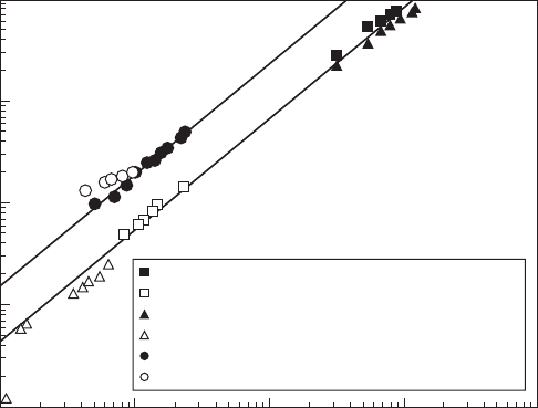
Handbook of dielectric, piezoelectric and ferroelectric materials544
w
2
= adδ 18.2
where δ is the domain wall width. In this case, rather remarkably, the equation
applies to all ferroics (ferromagnets, ferroelectrics and ferroelastics) with the
same coefficient (Catalan and Scott 2006):
a = [2π
3
/21ζ(3)] [χ(a)/χ(c)]
1/2
= 2.455 [χ(a)/χ(c)]
1/2
18.3
where χ(x) are the susceptibilities and ζ(3) the Riemann zeta function of
power 3.
In addition to understanding the static configurations of nano-domains,
we need to understand how their switching depends upon size. That brings
us to the 1962 Kay–Dunn law, which consists of an equally simple law for
the coercive field (minimum switching field E): E
c
= bd
–2/3
and coercive
voltage V
c
= bd
1/3
.
Both of these laws hold from macrosopic millimetre thickness d down to
ca. 2nm. Thus, surprisingly, much of the behaviour of nano-ferroeoectric
domains can be derived from bulk classical physics. However, the smallest
domains found in BaTiO
3
– 1.0nm – as well as three-dimensional nano-
domains – both violate the Kittel law, and recently Catalan has provided a
multi-dimensional extension of Kittel’s one-dimensional law that clarifies
this. Domains are usually studied in flat planes, but some [3D] nanodomains
are shown in Fig. 18.3. Another qualitative difference is that domain switching
in ferroelectrics of submicrometre lateral widths is much more determined
Schilling’s data on BaTiO
3
Streiffer’s data on PbTiO
3
Mitsui’s data on Rochelle salt (gradual cooling)
Mitsui’s data on Rochelle salt (sudden cooling)
Dumas’s data on Co
Sparks’s data on Ni
Thickness
1/2
(nm
1/2
)
10
4
10
3
10
2
10
1
10
0
10
0
10
1
10
2
10
3
10
4
18.2
Stripe width
w
vs. thickness
d
in PbTiO
3
, BaTiO
3
and Rochelle
Salt (Schilling
et al.
2006).
WPNL2204
Ferroelectric nanostructures for device applications 545
(rate-limited) by nucleation than by domain wall velocities, so that the early
theory of Pulvari and Kuebler (1958a,b), which included nucleation, works
better than does that of Landauer et al. (1956), as shown recently for Samsung
0.18µm
2
area PZT cells (Jung et al., 2005). Landauer et al. did not ignore
nucleation; actually they considered it and rejected it, because it would
imply an inductive (phase-lag) part of the switching response, and they
found none in their early experiments. Switching as fast as 280ps has been
demonstrated recently in thin PZT films (Li et al., 2004); however, this is for
small-area capacitors with very small load resistance and a very large driving
source – for real devices with 5V sources and a 10–100ohm load, 60ns is a
more realistic design access time (RC-limited).
Figures 18.4 and 18.5 illustrate nanostructures in thin ceramic films: Fig.
18.4 shows nanotubes; Fig. 18.5, 0.3 Tbit/in
2
nano-array of Pt-nanowires/
PZT. A rather interesting development in 2005-6 has been the attachment of
nano-capacitors onto the ends of a registered array of carbon nanotubes. This
was first done by Jang et al. (2005), using Si
3
N
4
as the dielectric for the
capacitor; more recently Kawasaki et al. (2007) in our Cambridge lab have
achieved this with a ferroelectric PZT capacitor rather than the non-switching
silicon nitride. In Figs 18.6 and 18.7 other non-planar complex nano-device
structures are shown: Fig. 18.6 is an SEM cross-section of a PZT/CFO
(cobaltous ferrite) magneto-electric composite (Ramesh, Berkeley); Fig. 18.7
shows atomic force microscopy (AFM) nano-writing (Paruch et al., 2006).
Tera-bit ferroelectric memories are not yet a reality: The state of the art
for hard-wired devices is a 0.3Tbit/in
2
PZT array on Pt-nanowires encased
200 nm
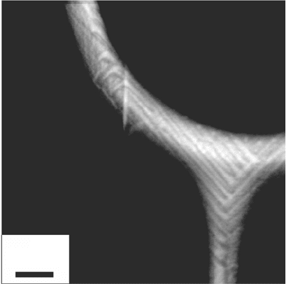
18.3
[3D] nano-domains in BaTiO
3
(Saad
et al
., 2006).
WPNL2204
Handbook of dielectric, piezoelectric and ferroelectric materials546
in meso-porous Al
2
O
3
(Evans et al., 2007). (An AFM-system 1Tbit/in
2
single-
crystal device was shown earlier by Cho et al., 2002). Such a 30nm diameter
capacitor still switches 1000–2000 electrons per bit, which is readable at
room temperature (and a good rule of thumb for minimum charge for sense
amplifier error-free detection – single-electron devices are definitely not
realistic in this context), but the registration shown in Fig. 18.4 is not sufficiently
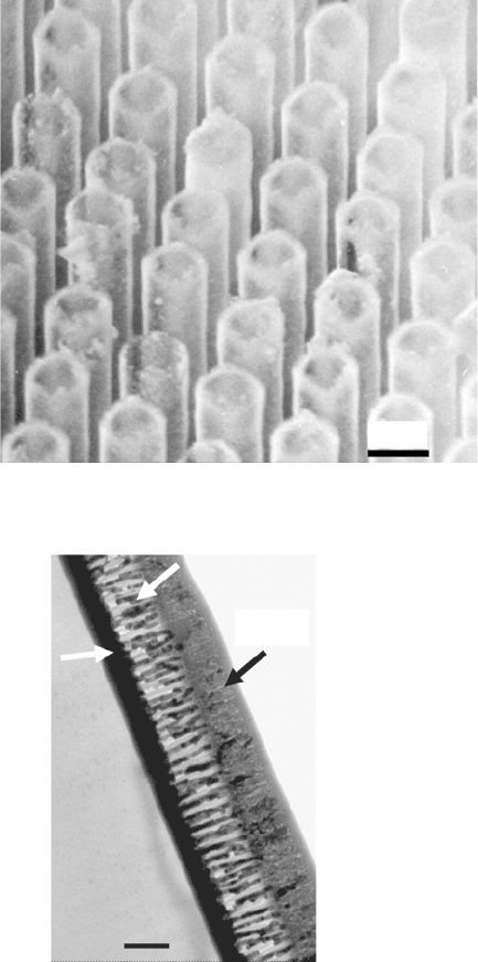
1 µm
18.4
SrBi
2
Ta
2
O
9
nanotubes (Morrison
et al
)2003).
Pt nanowires
BaTiO
3
Lower
electrode
Si
0.2 µm
18.5
0.5 Tbit/in
2
nano-array of Pt-nanowires/PZT (Evans
et al
., 2007).
WPNL2204
Ferroelectric nanostructures for device applications 547
long range to make a commercial device, and the prototype wiring has no
individual bit-line interconnects. The problem of registration in mesoporous
alumina has been partially solved by Masuda and Fukuda (1995), who obtained
perfect registration over lengths >> 1µm. Figures 18.5–18.8 illustrate nano-
ferroelectrics fabricated as composites (Fig. 18.5) and from AFM writing
(Fig. 18.6), and via a focused ion beam (FIB) (Figs 18.7, 18.8). The Belfast
group has fabricated complicated [3D] nano-structures, including free-standing
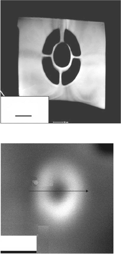
micro-rings from FIB (Fig. 18.8), and a 5 nm inside-diameter PZT nano-ring
(Fig. 18.9) within a pore of mesoporous Si done by chemical solution
deposition. It is important that on the nano-scale these devices can still be
20 nm
PFM
signal
(a.u.)
225 nm
17.7 Gbit/cm
2
18.6
Magneto-electric composite of CoFe
2
O
4
pillars in a BaTiO
3
matrix (Zheng
et al
., 2006).
18.7
AFM nano-writing on PZT (Paroch
et al
., 2001).
WPNL2204
Handbook of dielectric, piezoelectric and ferroelectric materials548
switched electrically or used for optical storage (Cho et al., 2002). Using
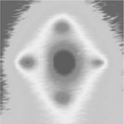
synchrotron sources (Fig. 18.10) one can study the structure of such very
thin films as functions of temperature and thickness. The 2004 32-Mb FRAM
from Samsung (PZT) or Matsushita (SBT) are still ahead of the commercial
MRAM development (4Mb MRAM from Freescale Co., July 2006), and
2 µm
18.8
Nano-toroid of single-crystal BaTiO
3
(Saad
et al
., 2006).
EDX line scan
10 nm
18.9
Ultra-nano-toroid of PZT inside a meso-porous Al
2
O
3
pore (Zhu
et al
., 2006 (EDX = energy dispersive X-ray analysis.).
WPNL2204
Ferroelectric nanostructures for device applications 549
Samsung has now (July 2006) a 64Mb FRAM. The ferroelectric-gate field
effect transistor (FET) offers non-destructive read operation, but short retention
times (maximum of a few days – Ishiwara et al., 2004) have thus far precluded
commercial products. A detailed comparison of MRAMs and FRAMs is
given by the author (Scott, 2007), including complex 4T-6C circuits in which
four transistors and six capacitors store each bit. Although the latter circuitry
prevents high-density RAMs, it permits non-destructive read-out.
18.3 Self-patterning
The two basic ways of fabricating nano-ferroelectric devices are, to use
industry jargon, ‘top-down’ – meaning submicrometre lithography – and
‘bottom-up’ – meaning self-assembly. The development of meso-porous silicon
and alumina (and GaN and GaAs) has presented experimentalists with templates
for the latter, and other techniques for coating nano-wires (Sebald et al.,
2005; Fan et al., 2006) have developed independently. Self-assembly of
nano-electrodes on ferroelectric films was first reported by Alexe et al.
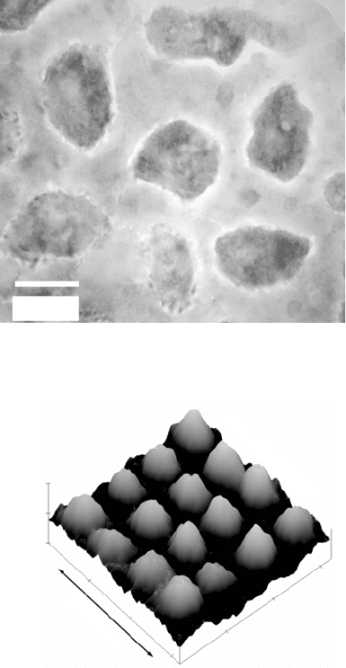
(1998) and in PZT nano-arrays, data and a model were published by Dawber,
et al. (2003b) (Fig. 18.11) based upon the original theory (Andreev, 1981)
that such islands would repel each other through their mutual strain interactions
with the substrate. Although self-assembly often results in arrays that have
only short-range order, complete registration satisfactory for commercial
RAM memory devices was achieved by Ma and Hesse (2004) via deposition
with inert spacers, such as mono-disperse submicrometre or micrometre-
18.10
In-plane diffuse X-ray scattering profiles around the PbTiO
3
<303> Bragg peak at 549 K (Auciello, 2006).
WPNL2204