Baca A.G., Ashby C.I.H. Fabrication of GaAs Devices
Подождите немного. Документ загружается.

Heterojunction bipolar transistors
f
max
~ 110 GHz
f
t
~ 60 GHz
h
21
U
gain (dB)
0
10
20
30
10
frequency (GHz)
1 100
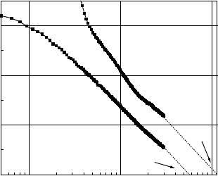
FIGURE 9.6 Plot of current gain, h
21
, as a function of frequency. The
extrapolated unity gain value gives the f
t
of the HBT.
9.2.2 Other GaAs HBT performance and
reliability issues
HBTs are a specific case of bipolar transistors where the emitter has
a wider bandgap than the base. The specifics of the device structure
will be introduced in Section 9.2.3. This subsection is a logical
continuation of Section 9.2.1 which will transition from tutorial
aspects of bipolar transistors to address some general performance
and reliability issues that affect high-performance GaAs HBTs.
Specific material and process issues that affect HBT performance
will be addressed in Sections 9.2.3, 9.5 and 9.6.
Thermal effects are extremely important considerations for
high-performance HBTs. Parameters such as f
t
and f
max
are often
found to peak at current densities near 10
5
Acm
−2
. It is often
observed that the DC current density also peaks near the same cur-
rent density. A typical power amplifier application might use 10
to 30 emitter fingers with dimensions of 2 × 30 μm
2
in a typical
cell. Assuming that drain voltage is 3 V, as for cell phone hand-
sets, each emitter finger dissipates up to 180 mW at the peak of the
RF signal. Such high power densities will result in large increases
in the junction temperature during operation of the power amp-
lifier. The close proximity of 10 or more emitter fingers would
add to the thermal load. Calculation of the junction temperature
depends on how the power is thermally dissipated. The follow-
ing equation establishes the relation between the temperature rise
and the power dissipated for an HBT sample in thermal contact to
a perfect heat sink, i.e. one that does not experience a temperature
rise in response to a thermal load:
T = R
th
I
C
V
CE
(9.4)
272
Heterojunction bipolar transistors
T is the junction temperature rise from the heatsink, R
th
is the
thermal resistance of the semiconductor and I
C
and V
CE
are the col-
lector current and collector-emitter voltage averaged over the RF
frequency. The thermal resistance R
th
is dependent on the geo-
metry and the thermal conductivities of the materials in contact
with the HBT.
GaAs is a poor thermal conductor compared to Si and to some of
the metals commonly used as interconnects, packaging materials
and heatsinks. Junction temperatures for GaAs HBT power ampli-
fiers can commonly attain and even exceed 150
◦
C. High junction
temperatures have important implications for device, processing
and reliability engineers. First, electron transport degrades with
increasing temperature. The thermal energy of common lattice
vibrations (phonons) increases with temperature and causes more
electron scattering. Both electron mobility and saturated velocity
decrease with increasing temperature. This negatively affects the
transit time of HBTs and, therefore, their high-frequency perform-
ance. Moreover, performance is temperature dependent, and due
to self-heating, HBTs will operate at different junction temper-
atures with different input-power levels. These thermal processes
affect the linearity of any semiconductor device. For applications in
which linearity is important (i.e. communications), thermal effects
must be managed carefully and HBTs may be used at current
densities well below what their performance maximum would dic-
tate. In other applications, linearity is less important (radars) and
HBTs are operated at higher current densities and higher junction
temperatures.
High junction temperatures also have the potential for acceler-
ating the aging of some of the material constituents of the HBT.
Chapters 6 and 7 discussed how GaAs reactions with many com-
mon contacts such as Au, Ni, Pt and other contact constituents
occur within minutes or seconds at temperatures between 300 and
400
◦
C. It is not unrealistic to expect that some of these reactions
can occur at temperatures of 150–200
◦
C if the time is long enough.
In HBT investigations, both thermal and current-density acceler-
ation are considered important factors that can affect reliability.
The classic reliability equation for the median (or mean) time to
failure (MTTF) was introduced in Chapter 2 and is given by
MTTF = A
0
exp(E
a
/kT) (9.5)
where E
a
is the activation energy, k is the Boltzmann constant,
A
0
is a constant and T is the absolute temperature. The median
time to failure is determined by testing a given set of samples until
half of them have failed. Reliability experiments are performed
273
Heterojunction bipolar transistors
at temperatures high enough to accelerate the failures so that the
MTTF is measurable within hundreds or thousands of hours. Extra-
polation to the expected junction temperature is then made with
EQN (9.5) if the activation energy is known. Such studies are
commonly performed for HBTs and some of the most significant
findings will be summarised in Section 9.8.
Performance degradation of GaAs HBTs past 150
◦
C is usu-
ally unacceptable and provides a common upper limit for HBT
junction temperatures. Thermal management solutions are sought
to keep below this upper junction temperature limit. Some com-
mon techniques in practice are the thinning of the GaAs substrate,
sometimes to as thin as 50 μm, and the use of a thermal shunt to
the emitter of the HBT. The thermal shunt is a thick electroplated
metal which contacts the emitter directly and therefore is situated
directly over the heat source.
As a practical matter, there are various theoretical and experi-
mental techniques to determine the R
th
of EQN (9.4) for a GaAs
HBT and manage its thermal properties. Theoretical approaches
can include using reasonable thermal simplifications to build
equivalent-circuit thermal models and using available material
parameters to optimise them. Theoretical approaches may also use
three-dimensional thermal solvers to optimise a thermal approach.
Experimental approaches require a determination of the junction
temperature and then measuring it as the power density of the HBT
is changed. Direct junction temperature measurement techniques
are often unsatisfactory because they lack the resolution and pos-
sibly also the accuracy to determine the hot spot of an HBT. For
example, an infrared image will smear the emitter image over sev-
eral microns from its true location and give an average temperature
over that area which is less than theactualpeaktemperature. Never-
theless, with skilled practitioners, they can still be useful. Indirect
methods are often electrical in nature. One common method is to
relate the temperature of the emitter-base pn junction to its bandgap
and to measure it in an actual deviceby monitoring the emitter-base
turn-on voltage and comparing to carefully calibrated structures.
HBT performance peaks at high current density, often near
10
5
A/cm
2
. As will be elaborated on in Section 8.7, reliability of
HBTs has been difficult to achieve for current densities greater than
2×10
4
A/cm
2
. As is the case for FETs, both bias and current stress
have the potential for degradingHBTs. Device engineers are forced
to make practical tradeoffs such as these between performance and
reliability considerations.
Other performance and reliability issues relate to materials
choices made for the HBT structure (Section 9.2.3). Specific
reliability issues involving base doping (carbon and beryllium),
274
Heterojunction bipolar transistors
emitter choice (AlGaAs or InGaP) and processing choices are
discussed in Section 9.7.
9.2.3 HBT device structure and material issues
Both AlGaAs and InGaP are suitable emitter materials for GaAs-
based HBTs. AlGaAs was used earlier because most MBE systems
lacked a phosphorus source in the early days and because MOCVD
development of HBTs lagged MBE. AlGaAs is not an ideal emit-
ter for an HBT because about two thirds of the change in bandgap
is manifested in the conduction band offset at compositions of
interest (below 45%). The conduction band spike can cause current
blocking in an HBT (by reducing the number of electrons injected
into the base), while a valence band offset to GaAs is more desir-
able. The effect of the conduction band profile on current blocking
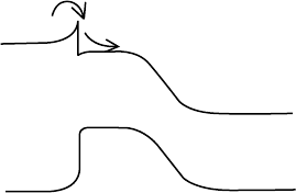
is illustrated in FIGURE 9.7. Contrasting with FIGURE 9.2, it
is clear that accounting for band bending due to the depletion
region at the emitter-base junction leads to a conduction band
spike at the E-B junction. Depending on the combination of the
conduction band offset and the emitter doping level, electrons may
traverse the spike by thermionic or thermionic field emission. Mod-
elling in one- or two-dimensions can be useful in assessing the
effect. AlGaAs emitters often use compositional grading gradu-
ally changing the Ga to Al ratio during growth to eliminate the
spike.
FIGURE 9.7 Conduction and
valence bands of a npn HBT with
band bending.
The bandgap of lattice-matched InGaP is near 1.9 eV. Both its
value and the conduction-band offset (E
C
) vary with the degree
of ordering in the InGaP, with E
C
ranging from 0.03 to 0.39 V.
The lower value is ideal for an Npn HBT, while the higher value is
not. The ordered state with a now uniform distribution of In and Ga
on the group III lattice site can be grown by MOCVD at relatively
high temperatures. The larger valenceband offset, E
V
, of ordered
InGaP is better suited to blocking the base-emitter hole current than
that for AlGaAs. However, AlGaAs has two practical advantages.
First, it is nearly lattice-matched to GaAs and slight variations
in composition do not introduce strain into the structure. Second,
there is no mixed group V chemistry to deal with for AlGaAs;
P and As intermixing may affect the quality of the InGaP/GaAs
interface. These advantages are slight and InGaP emitters have
gained favour in recent years to reduce back injection and for
processing and reliability reasons.
A typical structure is outlined in TABLE 9.1. The layers of the
emitter contain the intrinsic emitter layer (emitter-base junction),
the extrinsic emitter, which is a highly doped GaAs layer to trans-
ition to the contacts, and optionally a cap layer, which is often
InGaAs for a degeneratively doped layer for non-alloyed ohmic
275

Heterojunction bipolar transistors
TABLE 9.1 A typical epitaxial structure for GaAs HBTs.
Description Layer Composition Thickness (nm) Doping
Emitter cap InGaAs 50% 30 1–2 × 10
19
Ext emitter GaAs 100 2 × 10
18
Emitter (InGaP 49% In 50–70 5 × 10
17
or AlGaAs) 20–35% Al
Base GaAs 50–100 2–4 × 10
19
Collector GaAs 300–500 1–2 × 10
16
Subcollector GaAs 500–1000 2 × 10
18
Substrate SI GaAs
contacts. InGaP or AlGaAs are the common choices for the emitter
layer and they are generally doped in the mid 10
17
cm
−3
. Neither
the doping, the dopant used (usually Si), nor the thickness is crit-
ical, though they may have to be optimised in conjunction with the
rest of the structure. AlGaAs emitters are usually compositionally
graded to smooth the transition to the base (in order to eliminate
current blocking), but InGaP emitters are not, both because it is
more difficult and because it is less desirable with its smaller E
C
.
GaAs and InGaAs are the common choices for the extrinsic emit-
ter and the cap layers. Grading of the composition between the
binary and ternary alloys (GaAs/InGaAs, GaAs/AlGaAs) may be
employed to smooth the barriers to electron transport.
The base layer and the base/emitter interface are often the key
distinguishing features for the epitaxial growthofHBTs. High base
conductivity and fast transit times of the minority carrier electrons
across the base are required for high-frequency applications. These
requirements are at odds with their separate optimisation. Base
conductivity is increased with a thicker base layer and higher base
doping, while the minority-carrier transit time is inversely pro-
portional to the base thickness. Minority-carrier recombination
is increased with the higher base doping. These factors suggest
that an optimised solution will have thin base layers that are
highly doped. Fabrication and current gain specifications impose
practical limits that are within the ranges shown in TABLE 9.1.
Clearly, the quality of the epitaxial growth can affect the limits of
these ranges.
Many growers assess HBT material quality across different
laboratories by a metric defined as the current gain divided by
the base sheet resistance (in /square) to account for differing
base doping levels and thicknesses. This ratio is measured for a
large-area HBT (100 × 100 μm
2
emitter, for example) fabricated
with a triple-mesa process and measured at a current density near
800 A/cm
2
. A value near 0.4 is considered excellent [3].
276
Heterojunction bipolar transistors
Another quality factor arises from the need to keep sharp com-
position and doping profiles. Be, Zn and C are some choices for
doping the base, with Be being the historical dopant of choice
for MBE. Be diffusion becomes extremely problematic at com-
mon epitaxial growth temperatures at concentrations significantly
greater than the mid 10
18
cm
−3
and will smear the base-emitter
pn junction. Consequently, C doping was developed as an altern-
ative, first for MOCVD and later for MBE. Special procedures
were developed to limit Be diffusion in MBE and it has been used
in production by some major manufacturers. Often an undoped
GaAs spacer layer borders both the emitter and the doped base
layer. The thickness of this layer is of the order of 5 nm and it will
accommodate small amounts of diffusion. More significantly, most
MBE growers drop the temperature of the growth below 500
◦
C for
growing the base spacer and emitter layers to control Be diffusion.
C doping does not suffer from any diffusion problems. The main
issues with C are H incorporation during growth and build-up
of strain as the doping increases beyond 10
20
cm
−3
. Since fast
minority carrier recombination limits the practical doping level to
4×10
19
cm
−3
in all but the thinnest bases, strain issues are usually
secondary. H incorporation passivates the C acceptor, reducing the
base doping. If the C-H passivation complex is stable with time, its
effect can be calibrated out of the expected results. However, under
high current density, energetic electrons can impact the complex
and release free H. The C acceptors are depassivated and the hole
concentration then increases, which results in a reduced current
gain. In order to minimise this problem, the growth conditions
can incorporate a high-temperature process, either at the end of
the growth or during an interruption at some point in the emitter
growth, which serves to reduce the amount of incorporated H.
The growth of the collector involves a tradeoff between break-
down voltage and collector resistance. As seen from TABLE 9.1,
the collector doping is kept low to allow high breakdown, while the
subcollector doping is high to reduce the collector resistance. The
collector depletion width, w, is given by the expression
w = (2εε
0
(V
BC
+ V
bi
)/qN
Dc
)
1/2
(9.6)
where ε is the dielectric constant of the collector (GaAs: ε = 13.1),
ε
0
is the permittivity of free space (8.85 × 10
−14
F/cm), V
BC
is the
applied base-collector voltage, V
bi
is the built-in voltage of the
base-collector pn junction, q is the electron charge and N
Dc
is
the donor concentration of the collector. The collector doping is
chosen such that its dopant-dependent breakdown is sufficiently
high for the application of interest. Often, the collector breakdown
277
Heterojunction bipolar transistors
is designed to be equal to the intrinsic doping-level-dependent
breakdown or it can be designed such that a certain collector-base
bias results in complete depletion of the collector layer prior to
intrinsic breakdown. In the latter case, breakdown occurs in the
subcollector at slightly higher bias, a situation termed punch-
through. The collector resistance is minimised by making the
collector thin, consistent with the requirements for breakdown
voltage, and by doping the subcollector highly. The structure
of TABLE 9.1 will result in breakdown voltage in the range of
10–30 V.
GaAs is the most commonly used collector and subcollector
material. Highly doped InGaAs is not a reasonable choice for
a subcollector material because a thick layer is needed and the
lattice strain in such a layer will have to be accommodated by
lattice relaxation with the formation of misfit dislocations, which
will propagate upward as threading dislocations. However, it is
not uncommon to use thin etch-stop layers of InGaP near the
collector/subcollector interface or near the subcollector/substrate
interface for control of mesa etching or to allow selective undercut
(Section 9.6).
The vast majority of research and device development work
on HBT design is done by experimenting with the structure and
growth of HBTs. Some variations on the typical structure will be
briefly mentioned.
An electric field in the base can greatly increase the transit
time across the base (compared to diffusion) and improve high-
frequency performance. Two approaches to create a quasi-electric
field are the grading of the composition in the base (more Al near
the emitter or more In near the collector) and the grading of the dop-
ing (higher p-doping near the collector). Both of these approaches
create a gradient in the conduction band relative to the Fermi level
and aid in accelerating minority carriers through the base.
Another design approach is the use of a wide-bandgap collector
for higher breakdown voltage with a thin collector. InGaP is a
natural choice, but the base/collector interface must be optimised
to avoid current blocking.
Various approaches for engineering emitters have been tried.
One is to use a composite emitter. A thin InGaP interface with
the base is used for a fully depleted ledge (Section 9.5.1) with
an AlGaAs emitter above it. This type of structure is electric-
ally similar to an AlGaAs emitter and the main advantage is for a
selective wet etch that stops at the ledge. Another engineered emit-
ter approach is placing the pn junction in the GaAs (heterostructure
emitter).
Other design approaches that combine process and growth
methods will be described in Section 9.6.
278
Heterojunction bipolar transistors
9.2.4 Overview of HBT fabrication
In both the GaAs and the Si world, the bipolar transistor may be
expressed as a multitude of device designs with many permutations
of processes or materials. Field effect transistors certainly have
a number of permutations in some of the processes and materials,
but they tend to converge in function and implementation much
more than do bipolar transistors. It then becomes a real challenge
to present enough material of utility to a process engineer without
sinking hopelessly in the details. The choice of subject matter in
this chapter is weighted towards those devices and processes that
produce the most performance or reliability advantages. Many
other possibilities will be left as subjects for advanced study.
We will mainly discuss the fabrication of Npn (the conven-
tion is to capitalise wide bandgap layers) emitter-up HBTs. Much
research on collector-upHBTs existsin the literature because of the
possibility of achievinghigh f
max
by reducing C
BC
as in EQN (9.3).
However, the collector-up structure has suffered its share of prob-
lems such as low current gain due to injection from the emitter
into the extrinsic base and the difficulty of precisely etching down
to thin base layers of the same material (GaAs) as the collector. It
is not at the present a widely used technology.
The basic Npn process is a triple-mesa process. A schematic
illustration of the triple-mesa process is shown in FIGURE 9.8.
First an emitter metal is deposited (FIGURE 9.8(a)). Common
choices for the emitter metal are GeAuNi, TiPtAu and refract-
ory metals such as WSi. The choice of the emitter metal depends
on the strategy chosen for forming the emitter ohmic contact and
the emitter mesa etch. These issues will be discussed further in
Sections 9.3.1 and 9.4.1. In many cases, the emitter metal serves
as a mask for the emitter mesa etch (FIGURE 9.8(b)), which may
be a wet etch or a dry etch, depending on the feature size and
the dimensional control required. The base metal alignment and
evaporation is next (FIGURE 9.8(c)). Following the base ohmic
contact, the base mesa is patterned and etched (FIGURE 9.8(d)).
Again, both wet and dry etches may be used. The base mesa is
etched to isolate the base layer and expose the subcollector layer.
Collector ohmic contact and collector mesa processes follow the
base mesa (FIGURES 9.8(e) and (f )). The collector mesa etch will
isolate the subcollector region from the semi-insulating substrate.
Finally, the active device processing is completed by dielectric
passivation. A completed HBT integrated circuit process will also
include further thin film metal and dielectric layers for intercon-
nects, transmission lines and passive elements such as resistors,
capacitors and inductors. These interconnects and passive ele-
ments are deposited directly on the semi-insulating substrate or
279
Heterojunction bipolar transistors
E
B
B
semi-insulating substrate
E
C
B
C
B
E
C
B
C
B
semi-insulating substrate
semi-insulating substrate
semi-insulating substrate
semi-insulating substrate
E
semi-insulating substrate
E
E
B
B
(d)
(e)
(f )
(a)
(b)
(c)
FIGURE 9.8 The steps of a triple mesa HBT process: (a) emitter metal
deposition, (b) emitter mesa etch, (c) base metal deposition, (d) base mesa
etch, (e) collector metal deposition and (f) collector mesa etch.
on a suitable insulating dielectric. These non-active steps will not
be further considered in this chapter.
Device engineers will have to choose between self-aligned and
non-self-aligned emitter schemes. The self-aligned process uses
the emitter metal as a shadow mask for the base metal evaporation
to place the base ohmic contact in close proximity to the intrinsic
emitter and therefore lower the base resistance. The self-aligned
process is also efficient in minimising the total area needed for
the base mesa and thus minimising C
BC
. These factors can lead to
higher f
max
as described in EQN (9.3). The self-aligned process
also leads to several drawbacks. First, it places strict demands on
the processing. During the emitter etch, a controlled amount of
undercut of the emitter metal is required to prevent shorting of the
base and emitter without severely undercutting the emitter metal.
For short emitter widths, the consequences of excess undercut can
be the loss of mechanical support of the emitter metal. Second,
280
Heterojunction bipolar transistors
the self-aligned process reduces the current gain, β, of the HBT
because of the proximity of the base contact to the intrinsic emit-
ter region. The base/contact interface recombination velocity is
even greater than the recombination velocity of the free GaAs sur-
face. Since the HBT will be required to have a certain minimum
β, the relative merits of self-alignment must be evaluated against
other aspects of the device design that impact the current gain. For
example, higher doping in the base layer will also improve R
B
and
reduce β. The device engineer may then have to choose between
a self-alignment scheme or increasing the base doping to push the
limit of the current gain specification.
Non-self-aligned processes can have quite good realignment
tolerances by using state-of-the-art optical lithography steppers.
Based on realignment tolerance of 0.15–0.2 μm, contact spacing
from the edge of the emitter metal can be as little as 0.25 μm. Such
good alignment tolerance allows one to control the base metal to
emitter spacing and avoid the need for a self-aligned process.
Many of the challenges of the active HBT fabrication steps
involve understanding the interplay between design and process.
It is not enough to know the etch chemistry for the layer that
needs to be etched. HBTs have at least one heterointerface and
typically two or three. Layers near the interface often do not
etch the way a bulk layer does. Implementation of etches for
specific device designs requires understanding of the surface
technology issues. The next section explores specific etches in
GaAs-based HBTs.
9.3 MESA ETCHING FOR GaAs-BASED HBTS
9.3.1 Emitter mesa etch
The key requirement for emitter etches is that they remove emit-
ter material to expose the base layer with minimal damage and
without excessive undercut. In the case of a self-aligned process,
a small amount of undercut of the emitter metal is needed so that
the contact shadows the emitter sidewall during the base metal
evaporation to prevent shorting to the emitter. Wet etches are suit-
able for larger emitter widths, while dry or combination wet and
dry etches may be more suitable for smaller width emitters. The
cross-over between wide and narrow emitters depends on the total
thickness of the emitter epitaxial layers, but is generally near the
1 μm range. Since the emitter is the smallest dimension in the
HBT, GaAs HBT dimensions have relaxed geometries compared
with GaAs FETs and Si devices. Emitter etch chemistry, discussed
in the next two sections, depends on the materials in the emitter
281