Baca A.G., Ashby C.I.H. Fabrication of GaAs Devices
Подождите немного. Документ загружается.

Heterojunction bipolar transistors
with electronic states, which in turn are associated with depletion
regions that can be considered a parasitic reduction in the emitter
dimensions. A dielectric covering of the emitter sidewalls can, in
principle, provide a similar surface modification to that of the emit-
ter ledges described in the preceding section, but none to date are
actually promoted for this purpose. Nevertheless, dielectric pas-
sivation provides an extremely important function. The exposed
emitter edges are extremely susceptible to environmental exposure
and damage. Thus, the current gain of an HBT may change, some-
times dramatically, due to unpassivated environmental exposure.
The dielectric passivation provides a method of fixing the surface
condition of the emitter edges and preventing further changes due
to environmental contamination.
Silicon nitride is one common dielectric used for this purpose.
When deposited by plasma-enhanced chemical vapour deposition
(PECVD), it is mostly an amorphous combination of Si-Si, Si-N
and Si-H bonded complexes. Because oxygen is a common con-
taminant in PECVD, it is easily incorporated in amounts of several
percent. Ideally, silicon nitride is an amorphous or crystalline solid
of a single chemical entity, Si
3
N
4
, which chemically forms from
silane and ammonia precursors at temperatures near 700
◦
C. This
temperature is too high for GaAs processing because of the rapid
formation and desorption of As-oxides. Fortunately, PECVD and
related deposition methods, which can be used at temperatures of
300
◦
C and lower, provide chemically similar dielectrics, in terms
of the chemical properties that can stabilise dangling bonds at
the (Al)GaAs/dielectric interface. Nevertheless, specific process
issues associated with this dielectric can adversely impact HBTs
if they are not understood and addressed.
Through careful control of the emitter-edge surface preparation
during the emitter etch and subsequent surface cleans, an accept-
able condition is attained and stabilised by a suitable dielectric
deposition. The goal is to achieve a stable and acceptably high
current gain after dielectric passivation. The stability comes about
if the interface bonds, reconstructions and other relevant effects do
not change significantly over long periods of time and if the dielec-
tric prevents the diffusion of environmental contaminants that
could cause these changes. Silicon nitride has long been an excel-
lent choice for this type of passivation even though the scientific
understanding of what occurs at the interface is mostly lacking.
There is most certainly a need for process optimisation in which
current gain and high-frequency performance, reliability and other
considerations are monitored as a function of process conditions.
Often process conditions suitable for high-quality dielectrics in
other applications (dielectric interconnects, capacitors) are useful
starting points.
292

Heterojunction bipolar transistors
One major process issue arises because hydrogen can passivate
both n-type and p-type dopants in HBTs. PECVD silicon nitride
typically contains of the order of 25% hydrogen. That this amount
of hydrogen can be available and not cause HBT degradation prob-
lems is remarkable, but no lifetests to date have suggested that it
is a serious problem. However, it is important to recognise the
possible methods of degradation and test the HBTs with vari-
ous PECVD deposition conditions. Little of this type of research
has been reported in the literature. It has so far largely been left
to process engineers at each institution to optimise their own
processes. Some symptoms of hydrogen passivation have been
documented from reliability studies on devices with H-implant
isolation [6,7].
When p-type dopants are passivated in the base, the base sheet
resistance will increase due to reduced hole concentration and the
current gain will also increase (since recombination increases with
higher doping level). Likewise, the subcollector sheet resistance
will increase if n-type donors are passivated with H. Since some
of these effects occur with ion damage, which can also be present
in PECVD, RIE and high-density plasmas, it is necessary to do
carefully controlled studies.
An SiN passivation step will usually change the DC current
gain of a small-area HBT by a small amount (β changes by less
than 15%, typically), although before and after measurements
are not usually made. After the process steps of FIGURE 9.8,
large-area HBTs are usually measured. Small-area HBTs are usu-
ally not measured until after another interconnect metallisation
step. Large-area HBTs are affected much less than small-area
HBTs (typically β changes by a few percent) by SiN passivation
because of their large area-to-periphery ratio. Ledge-passivated
HBTs are also less affected by SiN passivation, since much of
the critical area where SiN interface modification can take place is
already protected. Nevertheless, subtle effectsare present with SiN
passivation, even in these cases. Piezoelectric effects induced by
SiN stress are one type of passivation effect to be considered. Such
an effect is illustrated in FIGURE 9.13 where the DC current gain
is both emitter-length and orientation dependent for a small-area
HBT without a ledge. Stress-induced electric fields cause differing
amounts of electron drift to the extrinsic base region and affect sur-
face recombination and DC current gain. The effect was of larger
magnitude for PECVD deposited SiN compared to ECR SiN for
comparable stress [8], indicating that ECR films are more benign
to the exposed HBT surfaces.
ECR SiON
emitter length (μm)
[011]
[011]
0 1020304050
10
20
30
40
50
DC current gain β
0
60
FIGURE 9.13 An example of
orientation and dielectric overlayer
effects in GaAs HBTs.
Dielectrics deposited with high-density plasmas (ECR and ICP)
often contain much less hydrogen, of the order of 10–20%.
However, we emphasise that mobile hydrogen is the concern,
293

Heterojunction bipolar transistors
and process conditions may produce acceptable films by either
deposition method.
9.5.3 Sulphur passivation
In the late 1980s, it was found that sulphur treatments of a GaAs
surface could drastically modify the GaAs surface and change
its electrical properties. The details of sulphur passivation are
presented in Chapter 3. It was quickly verified by HBT engineers at
different laboratories that this treatment reduced the surface recom-
bination of GaAs in the extrinsic base region and led to increases in
current gain for small emitter dimensions. Many different methods
of sulphur treatment were studied while seeking the best approach.
However, it was also quickly found that the sulphur-modified
GaAs surface was not stable and the current gain degraded in a
matter of hours in air without further treatments. This led to a
further search for a method of stabilising the sulphur passivation.
Although many promising results were achieved, none were found
satisfactory for stabilising the current gain increase in HBTs. Two
basic problems were never overcome. First, the sulphur-modified
surface was very sensitive to plasma exposure and was never sat-
isfactorily combined with dielectric passivation. Second, HBTs
operate at a junction temperature near 150
◦
C. Most of the chemical
treatments to the sulphur-modified surface were not stable at that
temperature.
9.6 VARIATIONS ON HBT PROCESSING
Many dozens of variations on HBT processes are possible. Some
of the more interesting and useful ones have been selected for
presentation in this section to give a flavour of how processing is
used to improve devices or tailor them for certain needs. As will
be seen, many examples exist where performance was enhanced
significantly.
BB
E
(a)
(b)
substitutional
emitter
FIGURE 9.14 A substitutional
emitter HBT process.
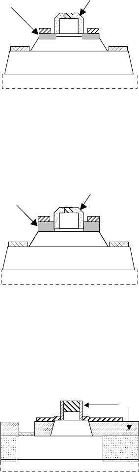
In Section 9.2.4, the basic triple-mesa process was described.
The standard method of fabricating a self-aligned emitter is
to use the emitter metal as an etch mask and as a shadow
mask for self-aligned deposition of the base metal. An altern-
ative self-aligned process involves defining the emitter using a
dielectric or photoresist mask. Then the emitter is defined by
wet or dry etching, preferably with undercut for metal shad-
owing (FIGURE 9.14(a)). After the emitter etch, the dielectric
(photoresist) mask is removed and base and emitter metals are
simultaneously evaporated (FIGURE 9.14(b)). This process is
294

Heterojunction bipolar transistors
feasible if an InGaAs cap layer is used for a non-alloyed ohmic
contact to the emitter.
A double-mesa process is sometimes used instead of a triple-
mesa one. A basic drawback of the triple-mesa process is the
introduction of significant topology from the various mesa steps.
As seen in the cross-section of FIGURE 9.3 and the dimensions
of the structure shown in TABLE 9.1, steps of approximately
2 μm are possible. The high-performance devices have minimal
dimensions for the mesa and ohmic metal widths. The step height
difference between different ohmic contact metals causes the
photoresist to spin with different thicknesses over the contacts.
High-resolution optical lithography steppers with near-UV sources
have limited depth of field, which makes it difficult to pattern high-
resolution features with different resist thickness and different
depths. Contact lithography tools will lack contact between the
mask and the resist at the lower elevation features (such as the col-
lector contact), which degrades resolution of the exposed feature.
These processing problems have reasonable solutions for GaAs
HBTs, but with a price of extra processing complexity. A double-
mesa process would use an implant for isolation of the subcollector.
The implanted species might be chosen from He, B, O, or F,
depending on the depth required and the implanter available. The
isolation mechanism would be through a damage-creation process
as described in Section 8.4. The double-mesa process is a reas-
onable way to minimise topography and has been widely used
(FIGURE 9.15).
E
C
B
C
B
semi-insulating substrate
FIGURE 9.15 A double mesa
HBT process.
Another possibility is to use ion implantation for isolation of all
layers for a quasi-planar process [6]. However, ion implantation
is not very effective for creating high-resistivity regions in highly
doped InGaAs. At theveryleast, InGaAs should be removedacross
the whole wafer during the emitter etch if it is used for an emit-
ter cap layer. A cross-section of a quasi-planar HBT is shown in
FIGURE 9.16. In this type of HBT process, the etching and metal
deposition for base and collector contacts generally occur within
the same lithography step.
E
C
B
C
B
semi-insulating substrate
FIGURE 9.16 A quasi-planar
ion implant isolated HBT process.
Hydrogen is an obvious element for the implant isolation pro-
cess because the thickness of the collector and subcollector to be
isolated can be close to 1.0 μm. The more common ion implanters
have an upper energy of 200 keV and only some of the light ele-
ments have a projected range in GaAs of greater than 1 μm. Atomic
hydrogen implants were a popular early choice for HBT isola-
tion, providing good isolation properties. Unfortunately, it was
found that the H was extremely mobile and easily moved across
the device to passivate donors and acceptors within the HBT. The
H-passivation complexes caused large changes in device operation
that were not acceptable to device engineers. Consequently, B or
295
Heterojunction bipolar transistors
O have been used instead of H for implant isolation, depending on
the projected range required and the implanter available.
E
semi-insulating substrate
C
B
C
B
diffused
base
SiO
2
FIGURE 9.17 A schematic
cross-section of an HBT with an
extrinsic diffused base.
Tradeoffs regarding base doping levels were discussed in
Section 9.2.2. High doping levels will improve high-frequency
analogue performance by reducing the base resistance, but they
also reduce the current gain by promoting recombination centres.
Another tradeoff is the desire for extremely thin base layers (to
improve transit times), while still maintaining the ability to etch
down to this layer and achieve reliable ohmic contacts that do
not completely react through the layer. One approach to improve
on these tradeoffs is doping the extrinsic base as illustrated in
the cross-section of FIGURE 9.17. A dielectric such as SiN/SiO
2
covers the patterned emitter metal. SiO
2
can be patterned over
WSi during the WSi etch, for example. After the emitter etch, a
dielectric sidewall is formed (to passivate and protect the emitter)
by a deposition and anisotropic etchback. Then Zn diffusion can
be used to increase the doping for the intrinsic base. An open-
tube diffusion using a ZnAs
2
source is one possibility for this
step. A temperature of 550
◦
C for 1 min results in a diffusion depth
of 80 nm and a sheet resistance of 385 /square [9]. The rest of
the HBT fabrication can proceed in any of the ways described
previously. Although the extrinsic base resistance is reduced by
this Zn diffusion, the base-collector capacitance may be increased
if the process is not optimised properly. The base and collector
doping levels typically differ by more than three orders of mag-
nitude, and it may be difficult to control the tail of the diffusion
into the collector. If the Zn tail converts part of the collector into
p-type GaAs, extrinsic C
BC
will go up as the collector distance
is reduced. Another concern is that Zn diffusion will degrade the
reliability.
E
semi-insulating substrate
C
B
C
B
regrown
base
SiO
2
FIGURE 9.18 A schematic
cross-section of an HBT with an
extrinsic regrown base.
Another method with the same goal of reducing the extrinsic
base resistance is to re-grow the extrinsic base [10]. Using a similar
emitter protection scheme as that for Zn diffusion (FIGURE 9.18),
the extrinsic base region is extended by selective regrowth of
p
+
GaAs using MOCVD. The emitter is protected with SiO
2
.
Then the extrinsic base is selectively regrown on the GaAs. Fab-
rication of the rest of the HBT occurs according to the methods
of FIGURE 9.8, for example. Although effective in principle,
regrowth methods for GaAs HBTs have not found the same accept-
ance as for laser diodes due to the more cost-sensitive nature of
HBT applications.
E
C
B
B
SiO
2
semi-insulating substrate
FIGURE 9.19 A schematic
cross-section of an HBT with a
buried SiO
2
dielectric.
As has been mentioned, methods to reduce C
BC
can take many
different forms. The method described next reduces the extrinsic
base area to a bare minimum and is illustrated in cross-section in
FIGURE 9.19. After emitter metal definition and emitter etch, a
thick dielectric sidewall (SiO
2
works well) is formed by deposition
296

Heterojunction bipolar transistors
and dielectric etchback. The thickness of the sidewall will be
proportional to the original thickness of the dielectric. The emit-
ter and sidewall will be the mask for a self-aligned base-mesa
etch. After another lithography step and collector isolation by ion
implantation, the outside of the base-collector junction is protec-
ted with dielectric by planarisation and etchback. An SiO
2
layer
is deposited and the device is planarised with a spin-coated film
such as photoresist. The entire structure is then etched back until
the base is exposed. A thin sidewall is then deposited (by dielec-
tric deposition and anisotropic etchback) to protect the emitter. The
base metal is formed next. An etchable metal like WSi is deposited
over the entire wafer and etched after protecting the base area with
photoresist. The base ohmic contact is non-alloyed and extends
little more than a transfer length from the emitter edge. At the
same time, it is supported and isolated from the collector by a
dielectric. Formation of the active elements of the HBT is com-
pleted after etching a window through the dielectric down to the
subcollector and depositing the collector ohmic contact. In order
to minimise plasma damage, an InGaP emitter can be left in place
until its removal just prior to the base metal deposition. In addition
to isolating the base from the collector, the buried SiO
2
has a lower
dielectric constant than GaAs and helps minimise extrinsic C
BC
.
This process was shown to achieve f
t
near 100 GHz and f
max
near
200 GHz for InGaP/GaAs HBTs [11]. Its primary disadvantage is
in the complexity and precision required during processing.
E
C
BB
semi-insulating substrate
subcollector
collector
(a)
(b)
E
C
BB
FIGURE 9.20 A schematic
cross-section of an HBT with a
selectively grown subcollector for
C
BC
reduction.
A selective buried subcollector has been used to enhance HBT
performance by reducing C
BC
as in EQN (9.3). A subcollector is
grown by MOCVD or MBE and patterned by chemical etching.
A wet etch process followed by oxide removal is preferable for
subsequent regrowth. Using a sulphuric-acid-based etch yields a
subcollector mesa in the shape of a trapezoid. The rest of the
HBT structure can then be regrown by MOCVD. The HBT is then
fabricated with the desired process. A schematic cross-section of
the structure is illustrated in FIGURE 9.20(a). The base-collector
capacitance is defined by overlap between the base mesa and the
subcollector. As seen in the top view of FIGURE 9.20(b), the base
mesa and the subcollector mesa extend in opposite directions and
the overlap can be minimal. The base and collector mesa extend
more to the left side of the emitter to allow room for the base
contact, while the subcollector mesa extends more to the right
side of the emitter for the same reason. The process is implemented
by growing the subcollector first, patterning it by mesa etching,
and then regrowing the rest of the HBT structure. When the HBT
is processed, the step of one side of the subcollector lies very
close to the emitter, and care must be taken that the regrowth
does not create extra defects in this region as they will lead to
297

Heterojunction bipolar transistors
excessive recombination. An f
max
of 140 GHz was reported using
this process [12].
Another approach for making a selective buried subcollector
uses ion implantation instead of etching to define the subcol-
lector. This approach is completely planar and avoids regrowth
on a faceted mesa edge close to the emitter. However, it is difficult
to achieve the high conductivity necessary for the subcollector
by ion implantation in GaAs. Epitaxial growth is much more
effective for maximising the doping level and thickness compared
to ion implantation. Ion implanted, buried subcollector HBTs
with increased collector resistance will negate the benefit of a
reduced C
BC
.
E
C
B
B
semi-insulating substrate
subcollector
H
+
collector
implant
FIGURE 9.21 A schematic
cross-section of an HBT with deep
implants for C
BC
reduction.
Ion implantation has been used in another way to reduce the
base-collector capacitance. A deep H-ion implantation is used to
damage the conducting collector and subcollector region below the
extrinsic base, as illustrated in FIGURE 9.21. As in the case for the
regrowth method, one side of the subcollector is left intact along
with a narrow base metal and mesa. The other side of the subcol-
lector is implanted with only a small separation from the emitter
edge to reduce extrinsic C
BC
. The H-implant only minimally dam-
ages the extrinsic base because the surface concentration of the
damage profile is severaltimeslessthanthepeakdamageatthepro-
jected range for the H ion. Another shallower, lower-dose implant
can be used to damage the low-doped collector on the side of the
emitter without the subcollector implant. As for the selective bur-
ied subcollector process, the collector contact is made only on one
side of the emitter. With this type of process the subcollector resist-
ance can be expected to increase in excess of 1 M, while the base
resistance increases from 175 to 265 /square [13]. A separation
of 1.2 μm of the implant from the emitter was chosen to minim-
ise the damage to the intrinsic base region. An f
max
> 200 GHz
was achieved with this process [13]. Although these results are
impressive, hydrogen passivation of donors and acceptors is a ser-
ious reliability concern. Use of another ion instead of H will,
unfortunately, lead to greater damage to the base that may be
unacceptable.
Another method for minimising C
BC
utilises an undercut col-
lector, a technique borrowed from InP HBTs. Emitter metal, mesa
and base metal are formed as in the standard triple-mesa process.
After base-mesa lithography, the collector undercut is performed.
The key to this process is the design of etch-stop layers in the
collector and subcollector. InGaP or AlGaAs layers can be used
as the etch-stop layers. For the InGaP layers wet etching (e.g.
H
3
PO
4
:H
2
O
2
:H
2
O) selectivity can be used to achieve the desired
collector undercut profile. To undercut the AlGaAs layers, RIE
can be used. Active HBT fabrication is completed after collector
298

Heterojunction bipolar transistors
ohmic contact and collector mesa formation. A cross-section of
an HBT with collector undercut is illustrated in FIGURE 9.22.
Though this structure looks very unstable, the mechanical strength
of microstructures is often surprising. Hero results can be reported
with air as the dielectric for the gap between the extrinsic base
and the subcollector. An f
max
of 170 GHz has been reported for
this type of structure [14]. As a performance enhancement tech-
nique, the collector undercut method with an air gap is superior
to the previously described C
BC
reduction techniques. The pre-
viously described techniques used GaAs, with its high dielectric
constant, as the insulator beneath the extrinsic base and will have
greater parasitic capacitance.
E
semi-insulating substrate
B
CC
B
FIGURE 9.22 A schematic
illustration of an HBT with a
collector undercut etch.
9.7 RELIABILITY OF HBTS
HBT performance peaks at high current density, often at greater
than 10
5
A/cm
2
. However, reliability of HBTs has been difficult to
achieve for current densities greater than 2×10
4
A/cm
2
. In applic-
ations requiring high linearity, perhaps backing off on power levels
to the lower current density levels may be an acceptable solution.
However, many other applications would be better served with
higher current density devices. The need for greater performance
from reliable parts has spurred research into the degradation mech-
anisms and searches for improvements. Much has been learned
and progress continues to be made. This section will summarise
some of the important findings and current understanding of HBT
reliability. This information should be an important consideration
influencing many aspects of HBT processing.
Like FETs, both temperature and electric fields are important
stressors. Thermal stress is especially difficult in HBTs because of
self-heating effects in small emitters. Electrical stress is difficult
because of the varied and subtle ways that the effects manifest
themselves.
HBTs can fail by gradual degradation or by sudden failure.
A gradual degradation is typified by a 10–20% change in an
electrical parameter such as current gain. Depending on the applic-
ation, other electrical parameter changes such as V
BE
,I
C
or output
power, may provide the criteria for failure. Abrupt failure may be
preceded by little degradation or by gradual degradation.
As for FETs, thermal stress will cause HBTs to fail through
metal contact degradation. Also like the FET case, the thinnest act-
ive layers are the most susceptible to degradation. Activation ener-
gies are high for contact degradation mechanisms (1.3–2.0 eV).
A number of ohmic contacts that degrade with this activation
energy contribute to high reliability even for thin layers, if properly
299
Heterojunction bipolar transistors
implemented. Some of these were described in Section 9.4. They
can generally be optimised to last hundreds of hours at 300
◦
C,
which extrapolates to millions or more hours at 150
◦
C.
The most common mode of HBT degradation is gradual β
decrease, with device failure commonly defined as a percent-
age degradation from the initial value (10–20%, commonly).
Though many specific types of failure are reported, two mechan-
isms receive the most attention: H passivation (and depassivation)
effects and recombination-enhanced-defect-reaction (REDR).
These will be discussed in order.
Hydrogen is known to passivate donor and acceptor impurit-
ies in many semiconductors, including GaAs. In HBTs, MOCVD
growth is known to incorporate H in the base layer when it is
C-doped. H incorporation at about 20% of the C level is not
unusual. The H incorporates as C-H complexes, which act as pas-
sivated acceptors. The C-H complexes can dissociate thermally,
which is probably what happens to 80% of them at MOCVD
growth temperatures (near 600
◦
C). They will also dissociate in
the presence of electrons that diffuse from the base according to
the reaction:
CH = C
−
+ H
+
(9.8)
The C
−
and H
+
can be electrostatically bound and quasi-stable
in the absence of electrons. Creation of these types of complexes
in the first moments of HBT operation causes an initial drop in cur-
rent which has been explained by H
+
acting as a recombination
centre as follows [15,16]:
H
+
+ e = H
0
(9.9)
H
0
+ e = H
−
(9.10)
H
0
or H
−
either do not act as recombination centres or diffuse
away from the base region. The electrical effect is that HBTs with
C-H complexes in the base show a decrease in β during initial
operation. As time passes the number of C-H complexes slowly
decreases as the reaction in EQN (9.8) proceeds, leading to an
increase in p-type doping in the base of the HBT. The current gain
of the HBT decreases further in response to increasing C-doping.
The former short-term effect can be dealt with through a burn-in
process, while the latter long-term effect is a reliability issue. The
fact that both thermal energy and electrons dissociate C-H com-
plexes implies that both electron density and junction temperature
are important factors in characterising the kinetics and reliability
implications of H-incorporation in HBTs. Although most reliab-
ility studies emphasise current gain, H-depassivation also lowers
V
BE
(the base-emitter turn-on voltage).
300
Heterojunction bipolar transistors
This reliability issue is dealt with either by removing the source
of hydrogen from the growth chemistry of the HBT or by remov-
ing the hydrogen after growth. By using MBE instead of MOCVD
for the HBT growth, one incorporates much less hydrogen. For
MOCVD growths, one resorts to post-growth annealing at tem-
peratures near 650
◦
C to remove the hydrogen. The timing (i.e. if
an interrupted growth is used) and length of the anneal must be
carefully optimised to avoid degradation of other aspects of the
HBT structure.
After H-passivation effects, the REDR mechanism receives the
most attention. As the HBT is operated, a fraction of the electrons
injected into the base recombine non-radiatively. For example,
electrons can tunnel from the emitter into a midgap trap level; once
in this trap, the electron can recombine non-radiatively with holes.
A non-radiative recombination event involves releasing energy to
phonons, which carries a finite probability of rearranging the lat-
tice and creating another defect. The process has positive feedback
such that the generation of a point defect associated with a non-
radiative recombination centre leads to the generation of more
point defects associated with recombination centres. These point
defects can join together to form more extended defects and more
extended recombination centres which leads to the gradual degrad-
ation of the device. The best means of avoiding REDR is to start
with high-quality HBTs with low levels of initial recombination.
Well-optimised InGaP ledge passivation may be a good means of
achieving high-quality, low recombination HBTs.
Evidence from HBT reliability studies [17] indicates that HBT
degradation includes many similarities to LED degradation [18].
Activation energies associated with midgap trap formation are in
the range of 0.4–0.7 eV. Such low activation energies are prob-
lematic because long times may be required to reveal evidence
of degradation at reasonable temperatures. Attempts to acceler-
ate the process at high temperatures is likely to activate another
mechanism with a different (usually higher) activation energy and
mask the degradation due to REDR alone. The evidence seems
to suggest that high-quality HBTs that are free from degradation
with higher activation energies will ultimately show degradation
by REDR.
To the extent that the physics of REDR is accepted, it has import-
ant implications for the choice of emitter material for reliability
considerations. REDR can occur in the emitter and emitter-base
space-charge region if holes are injected into the emitter. AlGaAs
with a valence-band discontinuity of 0.13 eV for an abrupt emitter
and up to 0.25 eV for a graded emitter (25% Al), is a decent bar-
rier to hole injection. However, ordered InGaP has a valence band
discontinuity as high as 0.43 eV, leading to far less recombination
301