Baca A.G., Ashby C.I.H. Fabrication of GaAs Devices
Подождите немного. Документ загружается.

Heterojunction bipolar transistors
in the high-bandgap emitter. The larger bandgap of the emitter
leads to more energy associated with REDR and can negatively
impact reliability. Also, most AlGaAs is initially more defective
than InGaP making the incidence of REDR more likely. Today,
GaAs HBT reliability is an evolving story. However, the evidence
indicates that more progress is being made at this time in raising
the maximum reliable current density using InGaP emitters with
ledge passivation. Verification that the REDR mechanism is the
main limiting factor may suggest that the base doping levels need
to be considered and possibly lowered to provide the lower initial
recombination levels.
Another example of gradual degradation is dopant diffusion.
Beryllium diffusion into the emitter will extend the base-emitter
junction from the heterointerface into the wide bandgap material
and cause V
BE
shifts. Beryllium was the predominant early prefer-
ence for MBE doping of the base, but has largely been supplanted
by C-doping to avoid this problematic diffusion of the base dopant.
Nevertheless, Be-doped HBTs were designed to be reliable at cur-
rent densities of 25 kA/cm
2
by optimising the structure and growth
conditions, and by being conservative in rating the operating cur-
rent density [19]. Zinc doping in MOCVD has similar diffusion
concerns and has been supplanted by carbon doping.
Although we have focused thus far on gradual degradation of
HBT electrical parameters, some devices fail suddenly, as in
the case for LEDs and LDs. Failure modes include dislocation
propagation, dislocation loops and dark line defects. These defects
can be observed by electroluminescence and, with considerable
patience, TEM. The dislocations may have propagated from the
substrate or be the result of mechanical stress in the device. Low-
dislocation substrates are one means of minimising the former
type of propagation. Mechanical damage can result from stresses
arising during sawing, scribing or bonding the chip. They can also
result from process steps such as high-stress metals or other steps
that may induce strain. Studies of process-induced defects are little
more than exploratory case studies at this time. Relatively little is
known about the true origin of these types of defects.
After long-term bias-temperature stress, carbon precipitates
are sometimes observed in GaAs HBTs with a C-doped base.
For example, both AlGaAs/GaAs and InGaP/GaAs HBTs with
4 × 10
19
cm
−3
C-doping of the base were biased at 6 × 10
4
A/cm
2
at junction temperature (T
j
) of 150–260
◦
C [20]. After an ini-
tial burn-in, a stage of gradual β degradation resulted, followed
by an abrupt failure. InGaP/GaAs HBTs displayed both slower
gradual degradation and longer times until abrupt failure than
AlGaAs/GaAs HBTs. TEM analysis with EDX was performed
on some of the failed samples. Both C-precipitates and occasional
302
Heterojunction bipolar transistors
migration of metallic impurities were imaged by TEM/EDX for
the InGaP/GaAs HBTs. The C-precipitates were 10–15 nm in
diameter.
Another reported degradation mechanism of GaAs-based HBTs
is a microtwin-like defect [21]. It has been suggested that these
defects are similar to typical micro defects in hydrogenated Si, but
it is not presently known if they are H-related in GaAs.
Reliability studies of GaAs-based HBTs have provided useful
information that can guide certain technology choices. They have
provided useful guides to operating current-density ranges. Best
practice for the choice of ohmic contacts, base dopant, emitter
material, and ledge-passivation schemes is also indicated from
reliability studies. Information is readily available for minimising
H-passivation effects. Companies involved in high-volume pro-
duction run reliability evaluations on multiple lots every month
and unquestionably will have access to information about many
process choices that are not publicly available. Most reliability
issues, however, are poorly understood, including the origin of
various types of extended defects, the best methods of dielectric
passivation and the best ways of avoiding process-induced stress.
In addition, most device engineers are not satisfied with the limit-
ations on HBT current density and would agree that much remains
to be done.
9.8 CONCLUSIONS
GaAs HBTs are greatly affected by the unintentional introduction
of defects in certain key parts of their structure. These process-
sensitive parts of the HBT structure need to be understood and
controlled by process engineers. HBT operation, testing and per-
formance characterisation supply the basic information that mater-
ials, processing and device engineers need to solve and understand
the often complex material and process interactions. Reliability
characterisation is an equally important guide for HBT engineers
to the extent that such information is available. Many HBT process
choices are available and some of the main ones were reviewed
in this chapter. As in most facets of engineering, knowledge and
information are a starting point for a job that needs to be done
better than is now possible.
REFERENCES
[1] W. Liu [Handbook of III-V Heterojunction Bipolar Transistors (John
Wiley and Sons, New York, 1998)]
303
Heterojunction bipolar transistors
[2] W. Lui [Fundamentals of III-V Devices: HBTs, MESFETs, and
HFETs/HEMTs (John Wiley and Sons, New York, 1999)]
[3] N. Pan et al. [IEEE Electron Device Lett. (USA) vol.19 (1998) p.115]
[4] M.J. Cich, J.A. Johnson, G.M. Peake, O.B. Spahn [Appl. Phys. Lett. (USA)
vol.82 (2003) p.651]
[5] E. Neubauer, M. Mai, J. Wurfl, W. Osterle [Semicond. Sci. Technol. (UK)
vol.15 (2000) p.818]
[6] F. Ren, S.J. Pearton, W.S. Hobson, T.R. Fullowan, J. Lothian, A.W. Yanof
[Appl. Phys. Lett. (USA) vol.56 (1990) p.860]
[7] S.J. Pearton [Int. J. Mod. Phys. B (Singapore) vol.30 (1994) p.1247]
[8] A.G. Baca, C. Monier, P.C. Chang, R.D. Briggs, M.G. Armendariz,
S.J. Pearton [Solid-State Electron. (UK) vol.46 (2002) p.797]
[9] T. Nittono, K. Nagata, O. Nakajima, T. Ishibashi [IEEE Electron Device
Lett. (USA) vol.10 (1989) p.506]
[10] H. Shimawaki, Y. Amamiya, N. Furuhata, K. Honjo [IEEE Trans. Electron
Devices (USA) vol.42 (1995) p.1735]
[11] T. Oka, K. Hirata, K. Ouchi, H. Uchiyama, K. Mochizuki, T. Nakamura
[IEEE Trans. Electron Devices (USA) vol.45 (1998) p.2276]
[12] Y.-F. Yang, C.-C. Hsu, E.S. Yang, H.-J. Ou [IEEE Electron Device Lett.
(USA) vol.17 (1996) p.531]
[13] M.-C. Ho, R.A. Johnson, W.J. Ho, M.F. Chang, P.M. Asbeck [IEEE
Electron Device Lett. (USA) vol.16 (1995) p.512]
[14] W.L. Chen, H.F. Chau, M. Tutt, M.C. Ho, T.S. Kim, T. Henderson [IEEE
Electron Device Lett. (USA) vol.18 (1997) p.355]
[15] F. Ren, C.R. Abernathy, S.N.G. Chu, J.R. Lothian, S.J. Pearton [Solid-
State Electron. (UK) vol.38 (1995) p.1137]
[16] J.Y. Chi, K. Lu [IEEE Electron Device Lett. (USA) vol.19 (1998) p.408]
[17] T. Henderson [Microelectron. Reliab. (UK) vol.39 (1999) p.1033–42
[18] O. Ueda [J. Electrochem. Soc. (USA) vol.135 (1988) p.11C]
[19] D.C. Streit et al. [J. Vac. Sci. Technol. B (USA) vol.14 (1996) p.2216]
[20] O. Ueda [Microelectron. Reliab. (UK) vol.39 (1999) p.1839]
[21] H. Suguhara, J. Nakano, T. Nittono, K. Ogawa [GaAs IC Symp. Technol.
Digest (IEEE, Piscataway, NJ, USA, 1993) p.115]
304
Chapter 10
Wet oxidation for optoelectronic and MIS
GaAs devices
Chapter scope p.305
Mechanism of wet oxidation
processes p.305
Chemistry of wet and dry oxidation
of AlGaAs p.306
Electronic consequences of
oxidation processes p.307
Rates and profile evolution p.308
Al-mole-fraction effects p.310
Layer thickness effects p.313
Proximity enhancement effect p.314
Wet oxidation of other materials p.315
Miscellaneous observations p.317
Practical wet oxidation p.319
Applications in optoelectronic
devices p.321
Structural issues for oxide
VCSELs p.321
Defect-related issues for
optoelectronic devices p.324
Applications in electronic GaAs
devices p.325
Problems with wet and dry
oxidation for MIS devices p.325
GaAs-on-insulator applications p.326
Conclusion p.326
References p.327
10.1 CHAPTER SCOPE
Most of the post-growth fabrication issues of importance in making
electronic devices are equally applicable in making optoelectronic
devices. Many of the performance characteristics are grown in
by the specific design of mirror stacks, quantum-well numbers
and thicknesses, dopant profile distributions, etc. Post-growth pro-
cessing, with the exception of wet oxidation, is generally the same
as that of electronic devices. The previous chapters in this book
dealing with cleaning, passivation, etching and contact forma-
tion address the main requirements for fabricating optoelectronic
devices. The details of the technique of regrowth, which involves
etching a structure into a wafer and introducing it again into a
growth chamber for deposition of additional semiconductor layers
on the textured substrate, are beyond the scope of this book. To fab-
ricate top-surface gratings for a DFB (distributed feedback) laser,
proper mask alignment relative to the crystal axes and crystallo-
graphic etching can be used to form the grating, as discussed in
Section 4.3.2. Crystallographic etching can also be used to form
smooth, vertical mirrors with proper alignment of the mask relative
to a wafer’s crystal planes.
Because the principal additional fabrication technique for opto-
electronic devices is the wet oxidation of buried Al-containing
layers to make current apertures in VCSELs (vertical cavity sur-
face emitting lasers), this chapter will focus on that process. Both
fundamental issues and practical considerations for using a wet
oxidation process are presented here. The chapter concludes with
a discussion of attempts to make electronic devices, such as GaAs-
on-insulator (GOI) MESFETs and metal-insulator-semiconductor
(MIS) devices, using wet oxidation.
10.2 MECHANISM OF WET OXIDATION PROCESSES
The oxidation of Si has been the topic of exhaustive research
because of its importance in forming the Si/SiO
2
interface, the
305

Wet oxidation for optoelectronic and MIS GaAs devices
basis of CMOS technology. By comparison, the oxidation of GaAs
and AlAs is not as well understood. This section addresses some of
the fundamental chemical and physical properties that profoundly
affect the application of wet oxidation technology in GaAs devices.
10.2.1 Chemistry of wet and dry oxidation of AlGaAs
Dry oxidation of AlAs (and similarly of GaAs) can be described
relatively simply by
2AlAs + 3O
2
= Al
2
O
3
+ As
2
O
3
(10.1)
which presumably started with Al-O and As-O surface species.
In contrast, wet oxidation of AlAs or AlGaAs is much more
complicated.
Water can dissociatively adsorb on AlAs to give Al-O, Al-OH
and As-H. Some of the intermediate species in the wet oxidation
process and their evolution with oxidation time have been identi-
fied using Raman spectroscopy [1] and the following suite of reac-
tions [2] are consistent with the observedproducts of As and As
2
O
3
and the surface species formed by water adsorption. (Molecular
analogues, such as AsH
3
and AlO(OH), are used here to represent
surface species, such as As-H and Al-OH, so the thermodynamic
calculations are approximations to the actual situation.)
G
(kJ/mol
at 425
◦
C)
2AlAs + 3H
2
O
(g)
= Al
2
O
3
+ 2AsH
3
−451 (10.2)
2AlAs + 4H
2
O
(g)
= 2AlO(OH) + 2AsH
3
−404 (10.3)
2AsH
3
= 2As + 3H
2
−153 (10.4)
2AsH
3
+ 3H
2
O = As
2
O
3(l)
+ 6H
2
−22 (10.5)
As
2
O
3(l)
+ 3H
2
= 2As + 3H
2
O
(g)
−131 (10.6)
2AlAs + 3H
2
O
(g)
= Al
2
O
3
+ 2As + 3H
2
−604 (10.7)
2AlAs + 4H
2
O
(g)
= 2AlO(OH) + 2As + 3H
2
−557 (10.8)
The Gibbs free energy for these reactions depends on the temper-
ature; at 425
◦
C, all have a negative change in free energy, G,
which means that the reaction should proceed spontaneously if
not kinetically constrained. A general caveat should always be
remembered when discussing reactions in terms of their thermody-
namics. While thermodynamic calculations predict what reactions
will have negative changes in Gibbs free energy (G) and should,
306
Wet oxidation for optoelectronic and MIS GaAs devices
therefore, proceed spontaneously, the kinetics of the reactions
often determine what actually happens. If there is a high activation
energy (large E
∗
= large kinetic barrier) for a reaction, it may
proceed only very slowly, if at all, despite having a large −G.
The H
+
from water serves as the oxidising agent for the
low-oxidation-state Al in AlAs. As
2
O
3
is observed by Raman
spectroscopy as an intermediate in the reaction, but the elemental
H resulting from the reduction of the H
+
of water in the forma-
tion of Al
2
O
3
or AlO(OH) can react readily with As
2
O
3
to form
As. An analogous set of equations can be formulated for GaAs,
with AlGaAs being a composite of the two. Changes in the rel-
ative rates of formation and loss of these species can explain
most of the observations regarding composition dependence, time
dependence, layer shrinkage upon oxidation, changes in elec-
tronic properties in adjacent layers and the inability to form a
good GaAs/oxide interface for MIS devices. This will be discussed
further in Section 10.3.
The formation of elemental As is the most fundamental differ-
ence between wet and dry oxidation. It can readily volatilise as
elemental As or react with H to form AsH
3
, a gas under these
reaction conditions. Significant quantities of AsH
3
are not detec-
ted in standard wet oxidation processes, so formation of volatile
elemental As is apparently strongly favoured. Elemental analysis
of completely oxidised AlAs or AlGaAs shows that very little As
remains after oxidation. This loss of As favours formation of a
relatively porous oxide material that facilitates transport of react-
ants and products. This porosity enables a linear dependence on
time as the oxidation proceeds over relatively long distances, as
will be discussed in more detail in Section 10.3.
Wet oxidation of AlGaAs can be suppressed by addition of
even small amounts of oxygen to the gas. This may be due to
the preferential consumption of the reduced H-species by oxygen,
preventing formation of significant amounts of As. In the presence
of oxygen, the process proceeds like a dry oxidation even when
plenty of water vapour is present.
As
i
+Ga
Ga
As
Ga
+Ga
i
As
Ga
As
i
+V
Ga
As
o
GaAs + V
Ga
As
o
As
i
FIGURE 10.1 Defects generated
by free As atoms.
10.2.2 Electronic consequences of oxidation processes
While the generation of elemental As is highly desirable to permit
rapid, deep oxidation of an AlGaAs layer, the presence of free As
atoms is problematic for the electronic properties and crystallo-
graphic perfection of the semiconductor adjacent to an oxidised
layer. Some of the possible reactions with adjacent GaAs are illus-
trated in FIGURE 10.1. Arsenic atoms can react with the surface
Ga atoms, causing them to move forward onto a new lattice site
and leaving a Ga vacancy (V
Ga
) behind. Column III vacancies
307
Wet oxidation for optoelectronic and MIS GaAs devices
play an important role in enhancing interdiffusion, which can
degrade heterojunction interfaces. An As atom can diffuse into
the semiconductor as an interstitial As (As
i
). The As
i
can move
deeper into the semiconductor quite rapidly and undergo reaction
quite distant from the initial point of generation. The interstitial
can form anti-site defects (As
Ga
) by binding at vacant Ga sites or
by displacing a Ga from its site, forming a Ga interstitial (Ga
i
).
These defects quench luminescence. Arsenic precipitates result-
ing from the diffusion of interstitials have been observed at remote
interfaces (tens of nm away from the oxide) and even at the GaAs
surface of a wet-oxidised sample.
Problems due to defect-caused luminescence quenching and
intermixing at heterointerfaces in optoelectronic devices will be
discussed in Section 10.5.2. The importance of elemental As at
the oxide/semiconductor interface is especially problematic when
trying to achieve a very low interface-state density, as will be
discussed in Section 10.6.
10.3 RATES AND PROFILE EVOLUTION
The wet oxidation of AlGaAs can be understood in terms of the
classic model of Deal and Grove. In their model, the time depend-
ence of oxidation can be described as the sum of two terms:
d
2
/k
diff
+ d/k
rxn
= t where d is the oxidation depth and t is the
time. The linear term dominates when the oxidation is reaction-rate
limited and the parabolic term is dominant under diffusion-limited
conditions. In dry oxidation of AlGaAs, the parabolic, diffusion-
limited term is dominant and rates slow rapidly as the oxidation
front penetrates into an AlGaAs layer. However, it is most desir-
able to operate in the linear regime when trying to oxidise long
distances (tens and even hundreds of nm) very controllably and
in a relatively short time. Wet oxidation conditions can be found
that produce primarily linear, reaction-rate limited behaviour for
high Al-content AlGaAs. The specific conditions favouring linear
oxidation depend on both wafer temperature and AlGaAs mole
fraction and factors that favour linear rates are discussed below.
GaAs
GaAs
AlAs
a-Al
2
O
3
50 nm
FIGURE 10.2 Dense amorphous
interfacial layer at oxidation front
(TEM by R.D. Twesten).
The time dependence of the oxidation rate will be determined
by the relationship between the rate of formation of As
2
O
3
and its
conversion to As (EQNS 10.5 and 10.6 in Section 10.2.1) and the
subsequent rate of loss of As from the oxidised layer to leave
behind a relatively porous matrix of AlO
x
H
y
species, such as
Al
2
O
3
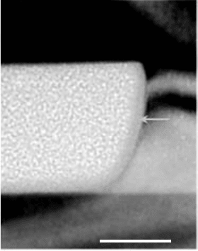
and AlO(OH). TEM studies have revealed the presence of
a thin (a few nm), dense amorphous region at the oxidation front
of a layer oxidised at 440
◦
C (FIGURE 10.2). Behind this dense
region lies a less dense region of amorphous AlO
x
H
y
that extends
308
Wet oxidation for optoelectronic and MIS GaAs devices
Al
2
O
3
AlO(OH)
AlGaAs
Al
2
O
3
As
2
O
3
Al
2
O
3
AlO(OH)
Al
2
O
3
As
2
O
3
AlGaAs
Al
2
O
3
AlO(OH)
AlGaAs
Al
2
O
3
As
2
O
3
or
(a)
(b)
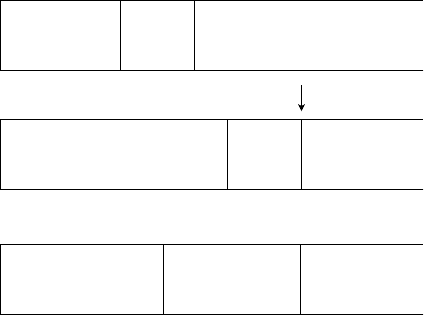
FIGURE 10.3 Evolution of oxide during wet oxidation of a layer: (a) linear:
fixed thickness of interfacial layer, (b) parabolic: increasing thickness of
interfacial layer [2].
back to the exposed mesa edge. The evolution of the thickness of
this dense interfacial zone as the oxidation penetrates deeper into
the layer will determine whether linear, parabolic or intermediate
time dependence is obtained [2], as illustrated in FIGURE 10.3.
There will be a dense layer at the oxidation front com-
posed mainly of AlO
x
H
y
and As
2
O
3
. When the reduction of
As
2
O
3
to As is sufficiently fast to balance the rate of forma-
tion of As
2
O
3
, this interfacial zone does not grow appreciably
in thickness as the oxidation front moves deeper into the layer
(FIGURE 10.3(a)).While this balance is maintained, a linear time
dependence will appear because the diffusional contribution to
the reaction rate does not increase significantly over the time
required to oxidise the device. If reaction conditions are changed
to preferentially increase the formation of As
2
O
3
relative to As
formation and loss, a steady increase in the thickness of the inter-
facial zone will occur (FIGURE 10.3(b)) and the diffusion-limited
parabolic time dependence will become dominant. Raman spectro-
scopy has shown a greater amount of As
2
O
3
to be present during
wet oxidation at higher temperatures, consistent with the trans-
ition from linear to parabolic behaviour as oxidation temperature
increases.
For extended reaction times at a given temperature, any
deviation from linearity will become increasingly obvious. For
conditions where the thickness is increasing only slowly, the
initial stages of the oxidation will closely approximate a linear
time dependence. This is usually observed with Al
0.98
Ga
0.02
As
under typical processing conditions, e.g. 30 min at 440
◦
C
for Al
0.98
Ga
0.02
As. Conditions producing faster oxidation tend
to tilt the balance in the direction of parabolic dependence.
309
Wet oxidation for optoelectronic and MIS GaAs devices
For oxidation rates of AlGaAs below 0.2 μm/min, the process
appears reaction-rate limited (linear) while initial rates above
1.3 μm/min appear diffusion limited at longer times. Thermody-
namic calculations of the temperature dependence of the important
As-based reactions predict that the formation of As
2
O
3
will
become increasingly favourable versus the reduction to As as tem-
perature increases. This is consistent with the generally observed
shift from linear towards parabolic behaviour with increasing
temperature for both AlAs (FIGURE 10.5) and Al
0.98
Ga
0.02
As
(FIGURE 10.6), as discussed in Section 10.3.1.
It is important to remember that wet oxidation of GaAs also
occurs although at a much lower rate. While the oxidation front is
advancing rapidly into the horizontal AlGaAs layer, the oxidised
layer is also slowly growing vertically into the bounding GaAs or
AlGaAs layers with lower mole fractions. Oxidation will occur
along the entire length of the oxidised channel, and the vertical
oxidation front will have progressed farther near the mesa edge,
where it has been exposed longer to the oxidising atmosphere.
If bounding layers are very thin, it is possible to oxidise completely
through them during long oxidation times.
Several factors strongly affect the rate of wet oxidation: Al mole
fraction, layer thickness and digital versus continuous-grade alloy-
ing. These plus the oxidation of materials other than AlGaAs will
be discussed in more detail.
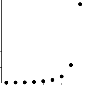
10.3.1 Al-mole-fraction effects
The addition of even small amounts of Ga to AlAs has a profound
effect on the wet oxidation rate [3], as illustrated in FIGURE 10.4.
Al mole fraction
0.84 0.88 0.92 0.96 1.00
0.0
0.2
0.4
0.6
0.8
1.0
normalised oxidation rate
425°C
FIGURE 10.4 Wet oxidation rate dependence on Al mole fraction.
310
Wet oxidation for optoelectronic and MIS GaAs devices
While Al
0.98
Ga
0.02
As has only a 2% differenceinAl content versus
AlAs, a 435% difference in the wet oxidation rate is observed. For-
tunately, it is commonplace to have sufficient control of Al mole
fraction during growth that deviation in oxidation rate due to com-
positional non-uniformity is generally not a problem. The 98%
composition is commonly used because it oxidises rapidly enough
to be convenient for making oxide apertures in VCSELs while
forming an oxide having greater mechanical robustness than that
obtained with pure AlAs. Another practical advantage is the reten-
tion of nearly linear time dependence of oxidation depth (distance
oxidised inward from the exposed mesa edge) for the depths and
processing conditions commonly employed, as will be discussed
below.
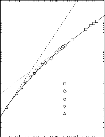
The wet oxidation of AlAs clearly displays the transition from
reaction-rate limited (linear versus time) to diffusion-limited rates
(parabolic) as the temperature is increased from 356 to 518
◦
C, as
illustrated in FIGURE 10.5 [4]. The dotted lines indicate the expec-
ted behaviour for a completely linear (d = kt) and completely
parabolic (d
2
= kt) oxidation. Since relatively minor changes in
temperature can have a pronounced effect on the time dependence
of the oxidised depth, AlAs is less attractive for device applica-
tions where precise control of oxidised depths is essential. Useful
0.1 1 10 100 1000 10000
0.01
0.1
1
10
100
518°C
468°C
418°C
356°C
380°C
t/(A
2
/4B) [1/mm]
x
o
/ (A/2) [mm/mm]
d
2
=kt
d=kt
AlAs
FIGURE 10.5 Temperature dependence of wet oxidation of AlAs from
Ochiai et al. [4].
311