Bhushan B. Handbook of Micro/Nano Tribology, Second Edition
Подождите немного. Документ загружается.

© 1999 by CRC Press LLC
z′(l) is also the tangent of the deflection angle. Using the definition of the moment of inertia for a beam
with a rectangular cross section,
(2.23)
where b is the width and h the thickness of the lever, one gets for the deformation z at the end of the
cantilever is related to the applied normal force F by
(2.24)
Hence, the compliance k
N
is
(2.25)
and a change in angular orientation of the end of
(2.26)
We can ask ourselves what will, to first order, happen if we apply a lateral force F
L
to the end of the
cantilever. The cantilever will bend sideways and it will twist. The sideways bending can be calculated
with Equation 2.24 by exchanging b and h
(2.27)
Therefore, the compliance for bending in lateral direction is larger than the compliance for bending in
the normal direction by (b/h)
2
. The twisting or torsion on the other side is more complicated to handle.
For wide, thin cantilevers (b h), we obtain
(2.28)
The ratio of the torsion compliance to the bending compliance is (Colchero, 1993)
(2.29)
where we assumed a Poisson ratio s = 0.333. We see that thin, wide cantilevers with long tips favor torsion
while cantilevers with square cross sections and short tips favor bending. Finally, we calculate the ratio
between the torsion compliance and the normal mode-bending compliance.
(2.30)
Ibh=
1
12
3
z
Eb h
F=
4
3
l
k
F
z
Eb h
N
==
4
3
l
∆
∆
α=
=
63
2
2
Ebh h
F
z
N
l
l
k
F
z
Eh b
Lb
L
,
==
∆ 4
3
l
k
Gbh
a
L,tor
=
3
2
3l
k
k
ab
h
L
Lb
,
,
tor
=
1
2
2
l
k
ka
L
N
,tor
=
2
2
l
© 1999 by CRC Press LLC
Equations 2.28 to 2.30 hold in the case where the cantilever tip is exactly in the middle axis of the
cantilever. Triangular cantilevers and cantilevers with tips not on the middle axis can be dealt with by
finite-element methods.
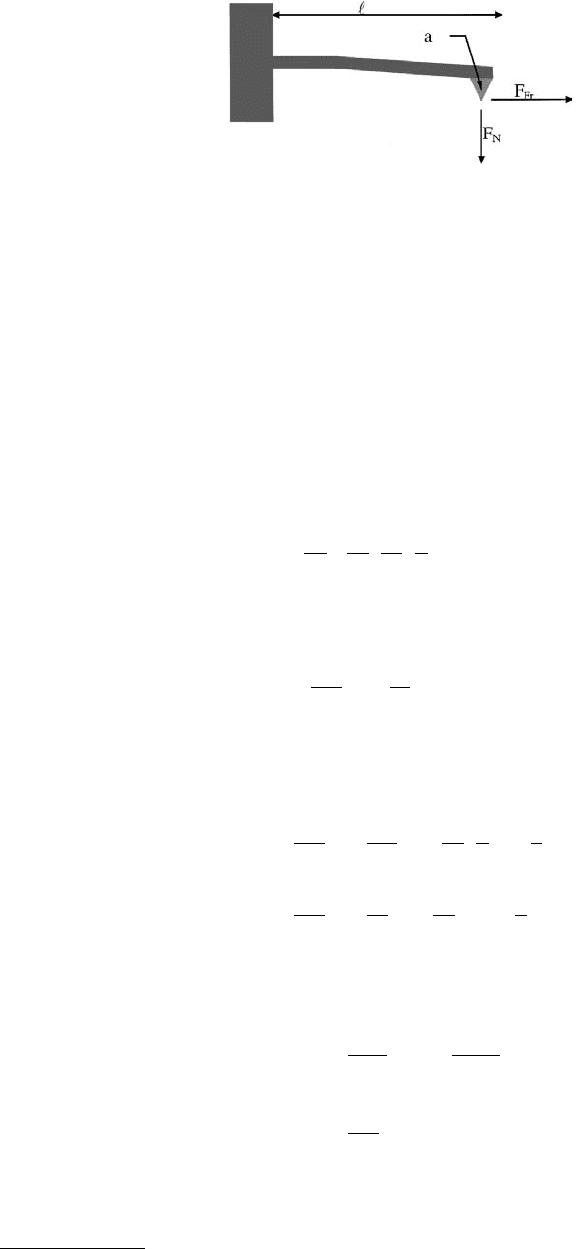
The third possible deflection mode is the one from the forces along the cantilever axis. Their effect
on the cantilever is a torque. The boundary condition for the free end of the cantilever is M
0
= a*F
Fr
(see
Figure 2.3). This leads to the following modification of Equation 2.19:
(2.31)
Integration of Equation 2.31 now leads to
(2.32)
A second integration gives the deflection
(2.33)
Evaluating Equations 2.32 and 2.33 at the end of the cantilever, we get the deflection and the tilt due to
the normal force F
N
and the force from the front F
Fr
(2.34)
These equations can be inverted. One obtains the two:
(2.35)
FIGURE 2.3 The effect of normal F
N
and frontal forces F
Fr
on a cantilever.
Mx xF Fa
N
()
=−
()
+l
Fr
′
()
== −
+
zx
dz
dx EI
xx
F axF
N
1
2
2
l
l
Fr
zx
EI
x
x
FaxF
N
()
=−
+
1
23
1
22
l
l
Fr
z
EI
F
a
EI
F
EI
a
FF
z
EI
F
a
EI
F
EI
aF F
NN
NN
l
lll l
l
llll
()
=− + = −
′
()
=− + = −
322
2
32 23
22
Fr Fr
Fr Fr
F
EI
z
z
F
EI
a
zz
N
Fr
=−
()
−
′
()
=−
()
−
′
()
()
12
2
2
32
3
2
l
l
ll
l
lll
© 1999 by CRC Press LLC
A second class of interesting properties of cantilevers is their resonance behavior. For cantilevered beams
one can calculate that the resonance frequencies are (Colchero, 1993)
(2.36)
with λ
0
= (0.596864 …)π, λ
1
= (1.494175 …)π, λ
n
→ (n + ½)π.
A similar Equation 2.36 as holds for cantilevers in rigid contact with the surface. Since there is an
additional restriction on the movement of the cantilever, namely, the location of its end point, the
resonance frequency increases. Only the λ
n
’s terms change to (Colchero, 1993)
with λ′
0
= (1.2498763…)π, λ′
1
= (2.2499997…)π, λ′
n
→ (n + ¼)π(2.37)
The ratio of the fundamental resonance frequency in contact to the fundamental resonance frequency
not in contact is 4.3851. For the torsion mode, we can calculate the resonance frequency to
(2.38)
for thin, wide cantilevers. In contact, we obtain
(2.39)
The amplitude of the thermally induced vibration can be calculated from the resonance frequency using
(2.40)
where k
b
is Boltzmann’s factor and k the compliance of the cantilever. Since force microscope cantilevers
are resonant structures, sometimes with rather high qualities Q, the thermal noise is not evenly distributed
as Equation 2.40 suggests. The spectral noise density below the peak of the response curve is
(2.41)
2.2.3 Tips and Cantilevers
The key to the successful operation of an AFM is the measurement of the interaction forces between the
tip and the sample surface. The tip would ideally consist of only one atom, which is brought in the
vicinity of the sample surface. The interaction forces between the AFM tip and the sample surface must
be smaller than about 10
–7
N for bulk materials and preferably well below 10
–9
N for organic macromol-
ecules. To obtain a measurable deflection larger than the inevitable thermal drifts and noise the cantilever
deflection for static measurements should be at least 10 nm. Hence, the spring constants should be less
than 10 N/m for bulk materials and less than 1 N/m for organic macromolecules. Experience shows that
cantilevers with spring constants of about 0.01 N/m work best in liquid environments, whereas stiffer
cantilevers excel in resonant detection methods.
ω
λ
ρ
n
n
hE
free
=
2
2
23
l
ω
ρ
0
2
tors
=π
h
b
G
l
ω
ω
0
0
2
132
tors,contact
tors
=
+
()
ab
∆z
kT
k
B
therm
=
z
kT
kQ
B
0
0
4
=
ω
in m Hz
© 1999 by CRC Press LLC
Building vibrations usually have frequencies in the range from 10 to 100 Hz. These vibrations are
coupled to the cantilever. To get an estimate, we use Equation 2.3. Inserting 100 Hz for the resonance
frequency and a spring constant of 0.1 N/m, we obtain an upper limit of the lumped effective mass m
eff
of 0.25 mg. The quality factor of this resonance in air is typically between 10 and 100. To get a reasonable
suppression of the excitation of cantilever oscillations, the resonance frequency of the cantilever has to
be at least a factor of 10 higher than the highest of the building vibration frequencies. This means, that
m
eff
has to be under any circumstances no larger than 0.25 mg/100 = 2.5 µg. It would be preferable to
limit the mass to 0.1 µg. This lumped mass m
eff
, however, is smaller than the real mass m, by a factor
that depends on the geometry of the cantilever.
A good rule of thumb says that the effective mass m
eff
is 9/20 of the real mass. Today, micro-machined
cantilevers are commercially available and are used almost exclusively.
2.2.4 Materials and Geometry
Cantilevers have been made from a whole range of materials (Pitsch et al., 1989; Akamine et al., 1990;
Grütter et al., 1990; Wolter et al., 1991; Colchero, 1993). Most common are cantilevers made of Si and
of Si
3
N
4
. As has been shown in Equation 2.25, Young’s modulus E and the density ρ are the material
parameters determining the resonance frequency, besides the geometry. The realizable thickness depends
on the fabrication process and the material properties. Grown materials such as Si
3
N
4
can be made thinner
than those fabricated out of the bulk.
The first row of Table 2.1 shows the different materials. The second row gives Young’s modulus. The
third row is the hardness, a quantity that is important to judge the durability of the cantilevers. The last
row, finally, shows the speed of sound, indicative of the resonance frequency for a given shape.
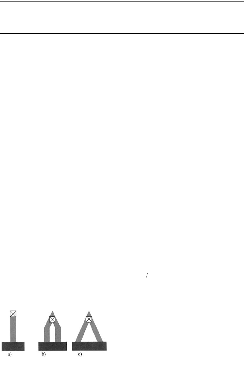
Cantilevers come basically in two shapes (Figure 2.4). Straight types are preferentially used for lateral
force measurements and noncontact modes. Their properties are rather easy to calculate. Triangular-
shaped cantilevers are easier to align. They are mostly made of silicon nitride. Their response to lateral
forces is more complicated.
Whereas type b must be calculated using finite-element methods, one can get a good estimate of the
normal force compliance of type c in Figure 2.4 using analytical methods. Using Equation 2.25 and
observing that the length of the two joined cantilever beams are l
2
eff
= l
2
+ (w/2)
2
, where w is the width
of the base of the cantilever, one gets for the compliance:
(2.42)
TABLE 2.1 Material Properties of Cantilevers
Diamond Si
3
N
4
Si W Ir Steel Au Al PMMA
E in GPa 1,000 300/180 110 410 530 200 80 70 2.5-3
Mohs Hardness 10 9 7 6 6–6.5 5–8.5 2.5–3 2–3 <1
c
long
in m/s 17,500 10,000 5,970 5,400 4,860 6,000 3,240 6,420 1,600
FIGURE 2.4 Shapes of cantilevers: (a) is preferentially used
for lateral force measurements and for noncontact measure-
ments; (b) and (c) are two types, mostly fabricated from
silicon nitride.
k
Ebh w
N
=+
3
2
2
32
24
l

© 1999 by CRC Press LLC
2.2.5 Outline of Fabrication
Most force sensors in use today or commercially available are manufactured either from silicon or
from silicon nitride. These two material systems are compatible with standard integrated circuit
processing techniques. The shape and the thickness are easily controlled with sub-100 nm precision.
This is necessary because the largest extension of the cantilevers is typically smaller than 300 µm.
Microfabrication techniques and batch processing are important prerequisites for any successful large-
scale production of force sensors.
The first published production recipe for cantilevers (Akamine et al., 1990) was for a sensor made of
silicon nitride. All silicon nitride levers available today are made more or less along the guidelines outlined
there. A silicon (100) wafer is thinned. Next, the tips are defined by masking the topside of the wafer
with oxide, leaving square openings with about 4-µm-long sides. They have to be oriented parallel to the
(110) directions. The silicon in these openings is attacked by the anisotropic etchant KOH. The etch
process is fastest parallel to the (111) surfaces. Therefore, a pyramidal-shaped depression is etched away.
Since the anisotropy of the etch rate is of the order of 100, the process slows down considerably once all
the sides of the pyramid meet. The etch process is then terminated.
In the next step the silicon nitride is grown on top of the silicon, on the side with the etch pits. The
thickness of the layer, together with the shape of the cantilever, determines the resonance frequency and
the compliance. Since the silicon nitride is grown, one has a very good control on the layer thickness.
Typically, cantilevers are 300 nm thick, or more. Calculated and experimentally verified spring constants
are of the order of 0.01 to 1 N/m. In a next step, Pyrex glass with openings for the cantilevers is bonded
from the topside onto the wafer. The remaining silicon is dissolved, leaving the cantilevers free. In the
last manufacturing step the cantilevers are coated with a thin reflective film, since most microscopes use
light reflected off the back of the cantilever to detect its deflection. Gold is usually used as the coating
material, together with a 1-nm layer of chromium as an adhesion layer.
The radius of curvature of silicon nitride cantilevers is limited to about 30 to 50 nm, because of the
manufacturing process. The imperfections of the etch pits and the filled-in silicon nitride limit the
sharpness. Silicon nitride tips can be sharpened during the production by thermal oxidation (Akamine
and Quate, 1992). Instead of directly depositing silicon nitride on the wafers with the pyramidal etch
pits, an oxide layer is deposited first. Then, the silicon nitride is added. When the oxide was removed
with buffered oxide etch, a sharpening effect was observed. Details of the process are described by the
inventors (Akamine and Quate, 1992). A second method is to grow in an electron microscope a so-called
supertip on top of the silicon nitride. It is well known that in scanning electron microscopes with a base
pressure of more than 10
–10
mbar hydrocarbon residues are present. These residues are cracked at the
surface of the sample by the electron beam, leaving carbon in a presumed amorphous state on the surface.
It is known that prolonged imaging in such an instrument degrades the surface. If the electron beam is
not scanned, but stays at the same place, one can build up tips with a diameter comparable with the
electron beam diameter and with a height determined by the dwell time. These tips are extremely sharp;
they can reach radii of curvature of a few nanometers. They allow therefore an imaging with a very high
resolution. In addition, they enable the microscope to image the bottoms of small crevasses and ditches
on samples. Unprocessed silicon nitride tips are not able to do this, since their sides enclose an angle of
90°, due to the crystal structure of the silicon.
Silicon nitride cantilevers are less expensive than those made of other materials. They are very rugged
and well suited to imaging in almost all environments. They are especially compatible to organic and
biological materials.
Alternatives to silicon nitride cantilevers are those made of silicon. The basic manufacturing idea is
the same as for silicon nitride. Masks determine the shape of the cantilevers. Processes from the
microelectronics fabrication are used. Since the thickness of the cantilevers is determined by etching
and not by growth, wafers have to be more precise as for the manufacturing of the silicon nitride
cantilevers.
© 1999 by CRC Press LLC
The first step in the process is a wet chemical etch to thin the wafer to a thin membrane (Wolter et al.,
1991; Kassing and Oesterschulze, 1997). The membrane thickness is adjusted such that it corresponds
to the lever thickness and the tip height (10 to 30 µm). The resulting membrane must be free of stresses.
The next step is to define the cantilever layout by reactive ion etching and by chemical etching, which
already creates freestanding cantilevers, as used later on in the microscopes. The third step is to define
the tip. One way starts with a small oxide cap at the place where the tip should be. The silicon is then
attacked by KOH. Its anisotropical etching characteristics then attack the silicon such that the protective
oxide cap is underetched. The art of cantilever manufacturing consists in timing this process such that
the silicon under the tip is just about to be etched away. The caps then fall down, and the rupture site
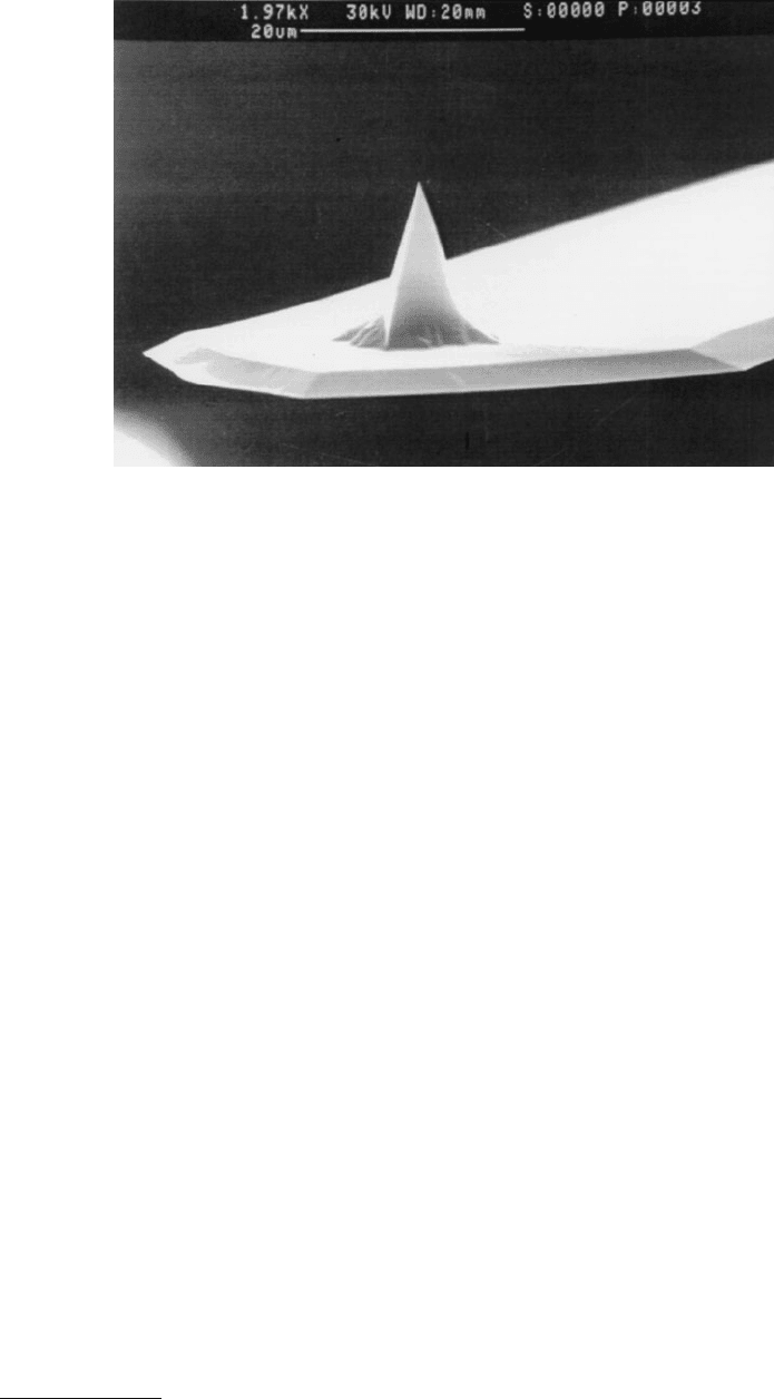
produces cantilevers with well-defined radii of curvature of 2 to 5 nm. An example of such a cantilever
is shown in Figure 2.5. The end section of the cantilever is shown. The lever is rounded to minimize
unwanted contacts of the lever edge with the sample. Improved fabrication processes have made it possible
to produce regularly tips with a radius of curvature of 2 nm. Tips, such as the one shown in Figure 2.6,
permit imaging at the highest resolution in all known imaging modes.
Since the thickness of the cantilever is determined by etching, it cannot be made as thin as in the
silicon nitride case. The lower limit is typically 1 µm. Therefore, the stiffness of the silicon cantilevers is
higher, ranging from 1 to 100 N/m. Since the material is a single crystal, unlike the silicon nitride, it has
a very high quality of the resonance. Values exceeding 100,000 have been observed in vacuum. Therefore,
silicon cantilevers are often used for noncontact or tapping mode experiments. The cantilevers have two
drawbacks when working in the contact mode. First, they have a very high affinity to organic materials.
They often destroy such samples. Second, their index of refraction matches the one of water rather closely.
Silicon cantilevers have a very poor reflectivity in aqueous environments.
There are efforts under way to make cantilevers of GaAs (Kassing and Oesterschulze, 1997). This
material is more difficult to process, but it would offer new advantages. GaAs is a direct band gap material.
Optoelectronic functions could be easily integrated into such cantilevers. The investigation of magnetic
properties could be improved by the use of spin-polarized tunneling.
Occasionally, cantilevers are made with tungsten wire or thin metal foils, with tips of diamond or
other materials glued to it.
FIGURE 2.5 A commercial cantilever from Nanosensors. (Courtesy of Nanosensors.)
© 1999 by CRC Press LLC
2.3 Optical Detection Systems
2.3.1 Interferometer
Soon after the first papers on the AFM (Binnig et al., 1986), which used a tunneling sensor, an instrument
based on an interferometer was published (McClelland et al., 1987). The sensitivity of the interferometer
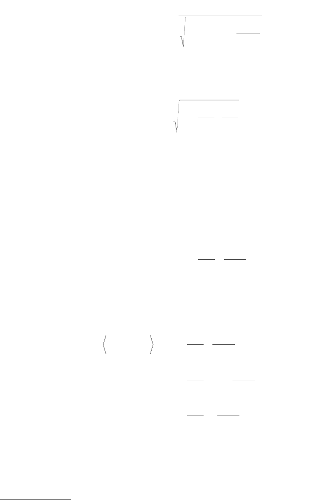
depends on the wavelength of the light employed in the apparatus. Figure 2.7 shows the principle of such
an interferometric design. The light incident from the left is focused by a lens on the cantilever. The
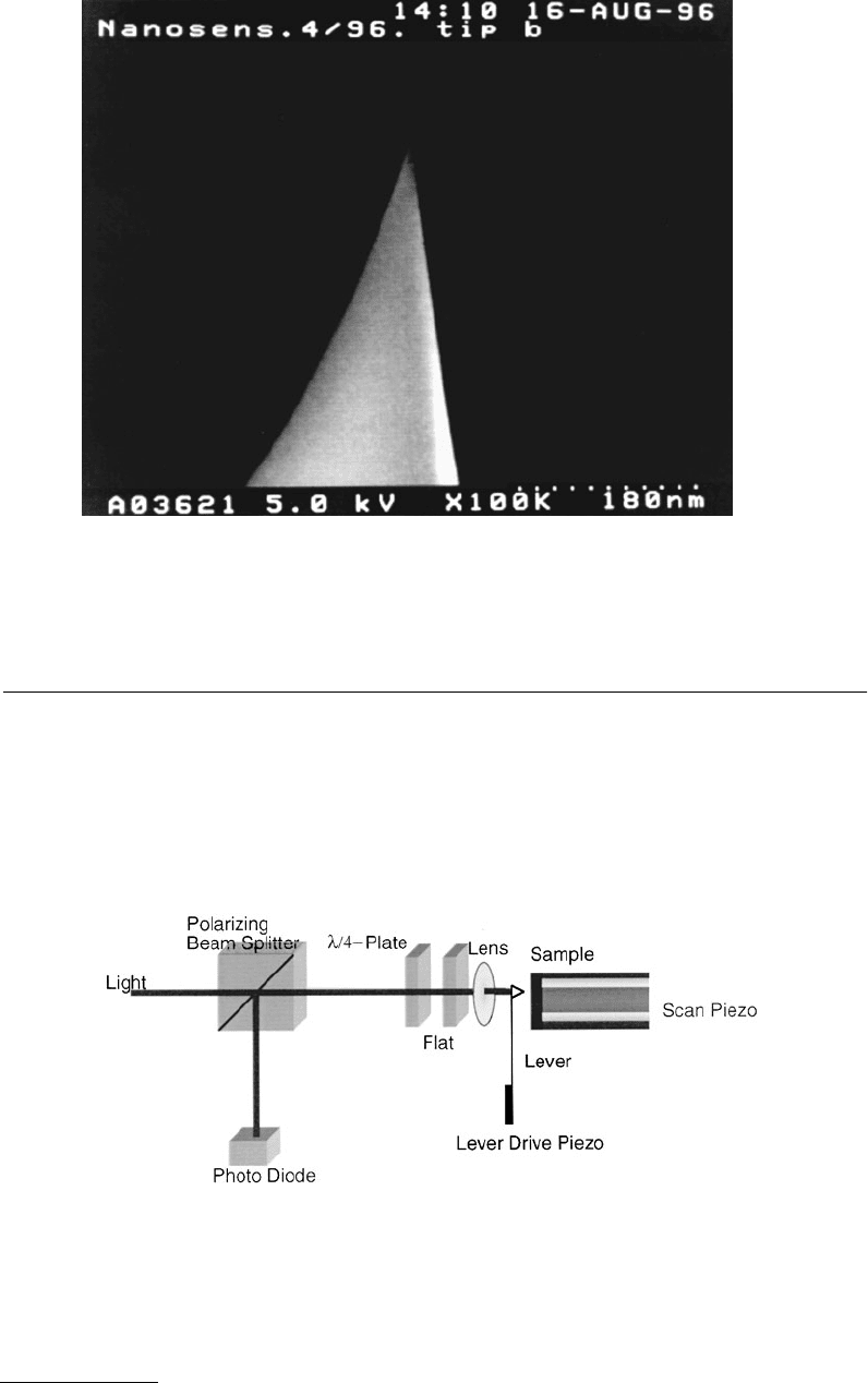
FIGURE 2.6 A SuperSharpSilicon™ tip from Nanosensors. The distance between two points on the scale in the
image is 18 nm. (Courtesy of Nanosensors. Used with permission.)
FIGURE 2.7 Principle of an interferometric AFM. The light of the laser light source is polarized by the polarizing
beam splitter and focused on the back of the cantilever. The light passes twice through a quarter wave plate and is
hence orthogonally polarized to the incident light. The second arm of the interferometer is formed by the flat. The
interference pattern is modulated by the oscillating cantilever.
© 1999 by CRC Press LLC
reflected light is collimated by the same lens and interferes with the light reflected at the flat. To separate
the reflected light from the incident light, a λ/4-plate converts the linear polarized incident light to
circular polarization. The reflected light is made linear polarized again by the λ/4-plate, but with a
polarization orthogonal to that of the incident light. The polarizing beam splitter then deflects the
reflected light to the photodiode.
2.3.1.1 Homodyne Interferometer
To improve the signal-to-noise ratio of the interferometer, the lever is driven by a piezoactuator near its
resonance frequency. The amplitude ∆z of the lever is
(2.43)
where ∆z
0
is the constant drive amplitude, Ω
0
the resonance frequency of the lever, Q the quality of the
resonance, and Ω the drive frequency. The resonance frequency of the lever is given by the effective
potential
(2.44)
where k is the spring constant of the free lever, U the interaction potential between the tip and the sample,
and m
eff
the effective mass of the cantilever. Equation 2.44 shows that an attractive potential decreases
the resonance frequency Ω
0
. The change in the resonance frequency Ω
0
in turn results in a change of the
lever amplitude ∆z (see Equation 2.43).
The movement of the cantilever changes the path difference in the interferometer. The light reflected
from the lever with the amplitude A
l,0
and the reference light with the amplitude A
r,0
interfere on the
detector. The detected intensity I(t) = {A
l
(t) + A
r
(t)}
2
consists of two constant terms and a fluctuating
term:
(2.45)
Here ω is the frequency of the light, δ the path difference in the interferometer, and ∆z is the instantaneous
amplitude of the lever, given according to Equations 2.43 and 2.44 as a function of the driving frequency
Ω, the spring constant k, and the interaction potential U. The time average of Equation 2.45 then becomes
(2.46)
Here all small quantities have been omitted and functions with small arguments have been linearized.
The amplitude of the lever oscillation ∆z can be recovered with a lock-in technique. However,
Equation 2.46 shows that the measured amplitude is also a function of the path difference δ in the
∆Ω ∆
Ω
ΩΩ
ΩΩ
zz
Q
()
=
−
()
+
0
0
2
2
0
2
2
2
0
2
2
Ω
0
2
2
1
=+
∂
∂
k
U
z
m
eff
2
44
00
AtAt AA t
z
tt
lr lr
() ()
=+
π
+
π
()
()
,,
sin sin sinω
δ
λλ
ω
∆
Ω
2
44
44
44
AtAt
z
t
z
t
z
t
lr
T
() ()
∝
π
+
π
()
≈
π
−
π
()
≈
π
−
π
()
cos sin
cos sin sin
cos sin
δ
λλ
δ
λλ
δ
λλ
∆
Ω
∆
Ω
∆
Ω
© 1999 by CRC Press LLC
interferometer. Hence, this path difference δ must be very stable. The best sensitivity is obtained when
sin(4δ/λ) ≈ 0.
2.3.1.2 Heterodyne Interferometer
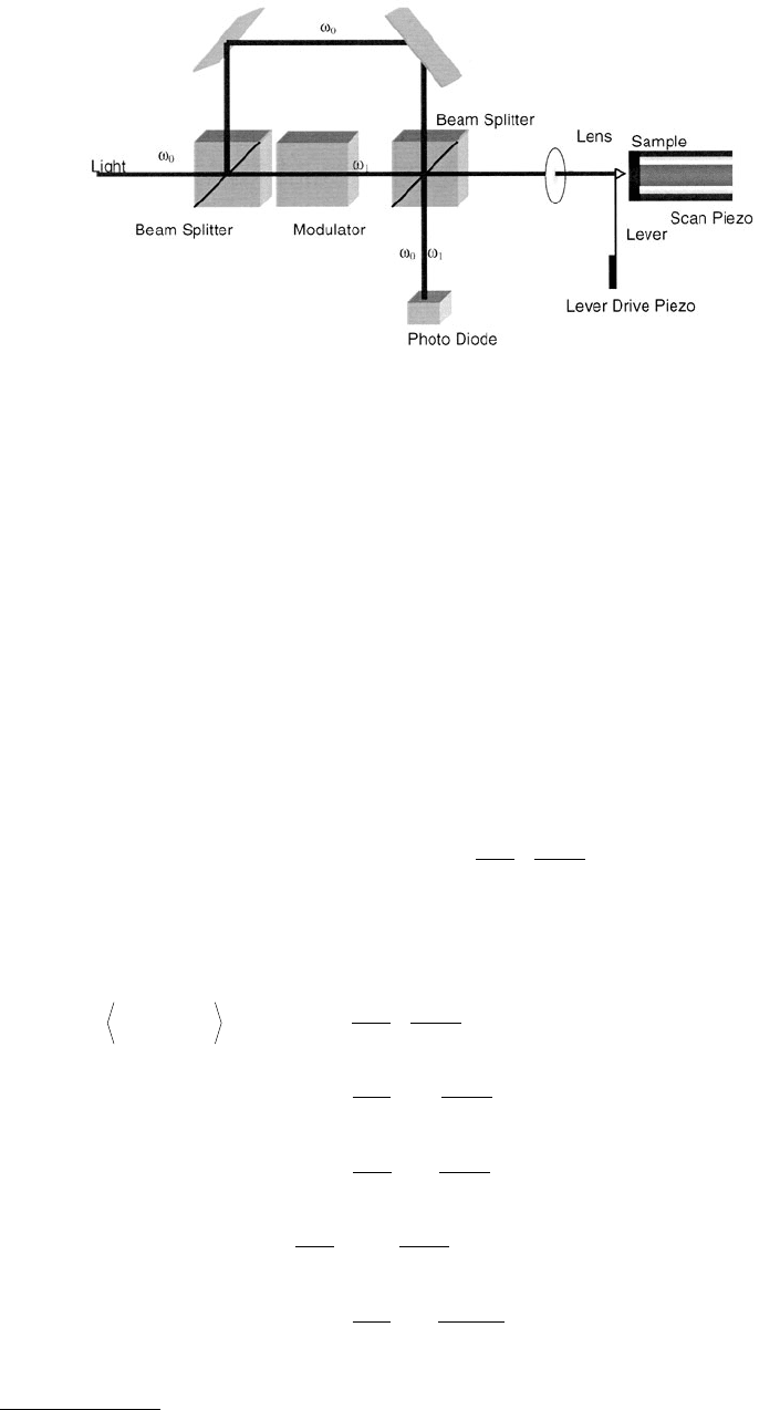
This influence is not present in the heterodyne detection scheme shown in Figure 2.8. Light incident
from the left with a frequency ω is split in a reference path (upper path in Figure 2.8) and a measurement
path. Light in the measurement path is shifted in frequency to ω
1
= ω + ∆ω and focused on the cantilever.
The cantilever oscillates at the frequency Ω, as in the homodyne detection scheme. The reflected light
A
l
(t) is collimated by the same lens and interferes on the photodiode with the reference light A
r
(t). The
fluctuating term of the intensity is given by
(2.47)
where the variables are defined as in Equation 2.45. Setting the path difference sin(4πδ/λ) ≈ 0 and taking
the time average, omitting small quantities and linearizing functions with small arguments, we get
(2.48)
FIGURE 2.8 Heterodyne interferometer AFM. Light with the frequency ω
0
is split into a reference path (upper
path) and a measurement path. The light in the measurement path is frequency shifted to ω
1
by an acousto-optical
modulator (or an electro-optical modulator). The light reflected from the oscillating cantilever interferes with the
reference beam on the detector.
2
44
00
AtAt A A t
z
tt
lr lr
() ()
=+
()
+
π
+
π
()
()
,,
sin sin sinωω
δ
λλ
ω∆
∆
Ω
2
44
44
44
4
AtAt t
z
t
t
z
t
t
z
t
tr
T
() ()
∝+
π
+
π
()
=+
π
π
()
−+
π
π
()
≈
π
cos sin
cos cos sin
sin sin sin
cos
∆
∆
Ω
∆
∆
Ω
∆
∆
Ω
ω
δ
λλ
ω
δ
λλ
ω
δ
λλ
δ
λ
−
π
()
≈+
π
−
π
()
sin sin
cos sin
4
4
1
8
22
2
∆
Ω
∆
∆
Ω
z
t
t
z
t
λ
ω
δ
λ
λ
© 1999 by CRC Press LLC
Multiplying electronically the components oscillating at ∆ω and ∆ω + Ω and rejecting any product except
the one oscillating at Ω, we obtain
(2.49)
Unlike in the homodyne detection scheme, the recovered signal is independent from the path difference
δ of the interferometer. Furthermore, a lock-in amplifier with the reference set sin(∆ωt) can measure
the path difference δ independent of the cantilever oscillation. If necessary, a feedback circuit can keep
δ = 0.
2.3.1.3 Fiber-Optic Interferometer
The fiber-optic interferometer (Rugar et al., 1989) is one of the simplest interferometers to build and
use. Its principle is sketched in Figure 2.9. The light of a laser is fed into an optical fiber. Laser diodes
with integrated fiber pigtails are convenient light sources. The light is split in a fiber-optic beam splitter
into two fibers. One fiber is terminated by an index-matching oil to avoid any reflections back into the
fiber. The end of the other fiber is brought close to the cantilever in the AFM. The emerging light is
partially reflected back into the fiber by the cantilever. Most of the light, however, is lost. This is not a
−
ππ
()
=+
π
−
π
+
π
sin sin
cos cos
44
48 4
22
2
∆
∆Ω
∆
∆
∆
z
tt
t
z
t
λ
ω
δ
λ
ω
δ
λ
λ
ω
δ
λ
()
−
π
+
π
()
=+
π
−
π
+
π
−
π
+
π
()
−
π
sin
sin sin
cos cos
cos cos
sin
Ω
∆
∆Ω
∆
∆
∆
∆
∆Ω
∆
∆
t
z
tt
t
z
t
z
tt
z
44
44 4
44
2
4
22
2
22
2
λ
ω
δ
λ
ω
δ
λ
λ
ω
δ
λ
λ
ω
δ
λ
λ
ωω
δ
λ
ω
δ
λ
λ
λ
ω
δ
λ
ω
δ
λ
tt
t
z
z
tt
+
π
()
=+
π
−
π
+
π
+
()
+
π
+−
()
+
π
+
4
4
1
4
2
2
4
2
4
2
22
2
22
2
sin
cos
cos cos
Ω
∆
∆
∆
∆Ω ∆Ω
ππ
+
()
+
π
+−
()
+
π
∆
∆Ω ∆Ω
z
tt
λ
ω
δ
λ
ω
δ
λ
cos cos
44
A
zz
tt
zz
tt
z
t
=−
π
+
()
+
π
+
π
=−
π
+
()
+
π
+
()
≈
π
2
1
4
2
44
1
4
2
8
22
2
22
2
∆∆
∆Ω ∆
∆∆
∆Ω Ω
∆
Ω
λ
λ
ω
δ
λ
ω
δ
λ
λ
λ
ω
δ
λ
λ
cos cos
cos cos
cos
(()