Bhushan B. Handbook of Micro/Nano Tribology, Second Edition
Подождите немного. Документ загружается.

© 1999 by CRC Press LLC
friction phenomena, and discuss the possibility of a frictionless “superlubric” state (Shinjo and Hirano,
1993; Hirano et al., 1997). Matsukawa and Fukuyama (1994) carry the process further in that they allow
both surfaces to adjust and examine the effects of velocity with attention to the three rules of friction
stated above. They argue, not based on their calculations, that the Bowden and Tabor argument is not
consistent with flat interfaces having no asperities. Since an adhesive force exists, there is a normal force
on the interfaces with no external normal load. Consequently, rules of friction 1 and 2 break down. With
respect to rule 3, they find it restricted to certain circumstances. They found that the dynamic friction
force, in general, is sliding velocity dependent, but with a decreasing velocity dependence with increasing
maximum static friction force. Hence, for systems with large static friction forces, the kinetic friction
force shows behavior similar to classical rule 3, above. Finally, Zhong and Tomanek (1990) performed a
first-principles calculation of the force to slide a monolayer of Pd in registry with the graphite surface.
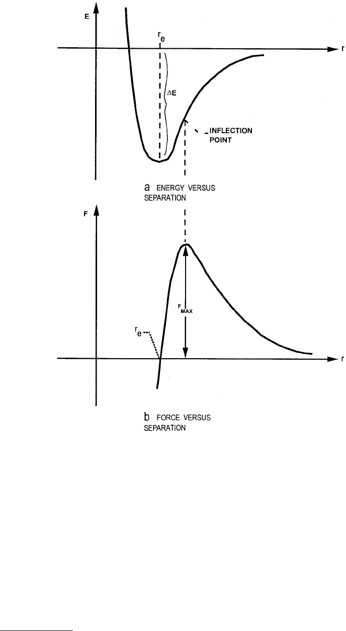
FIGURE 3.10
Example of a binding energy curve: (a) energy vs. separation; (b) force vs. separation. (From Banerjea,
A. et al. (1991), in
Fundamentals of Adhesion
(Liang-Huang Lee, ed.), Plenum Press, New York. With permission.)
© 1999 by CRC Press LLC
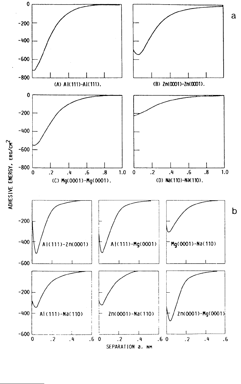
FIGURE 3.11
Adhesive energy vs. separation: (a) commensurate adhesion is assumed; (b) incommensurate adhe-
sion is assumed. (From Rose, J.H. et al. (1983),
Phys. Rev. B
28, 1835–1845. With permission.)
© 1999 by CRC Press LLC
Assuming some energy dissipation mechanism to be present, they calculated tangential force as a function
of load and sliding position.
Sokoloff (1990, 1992, and references therein) addresses both the friction force and frictional energy
dissipation. He represents the atoms in the solids as connected by springs, thus enabling an energy
dissipation mechanism by way of lattice vibrations. He also looks at such issues as the energy to create
and move defects in the sliding process and examines the velocity dependence of kinetic friction based
on the possible processes present, including electronic excitations (Sokoloff, 1995). Persson (1991) also
proposes a model for energy dissipation due to electronic excitations induced within a metallic surface.
Persson (1993, 1994, 1995) addresses in addition the effect of a boundary lubricant between macroscopic
bodies, modeling fluid pinning to give the experimentally observed logarithmic time dependence of
various relaxation processes. Finally, as more fully covered in other chapters of this book, much recent
effort has gone into modeling specifically the lateral force component of the probe tip interaction with
a sample surface in scanning probe microscopy (e.g., Hölscher et al., 1997; Diestler et al., 1997, and
references therein; Lantz et al., 1997).
In conclusion, while these types of simulations may not reflect the fully complexity of real materials,
they are necessary and useful. Although limited in scope, it is necessary to break down such complex
problems into isolated phenomena which it is hoped can result in the eventual unification to the larger
picture. It simply is difficult to isolate the various components contributing to friction experimentally.
3.4 Experimental Determinations of Surface Structure
In this section we will discuss three techniques for determining the structure of a crystal surface, low-
energy electron diffraction (LEED), high-resolution electron microscopy (HREM), and field ion micros-
copy (FIM). The first, LEED, is a diffraction method for determining structure and the latter two are
methods to view the lattices directly. There are other methods for determining structure such as ion
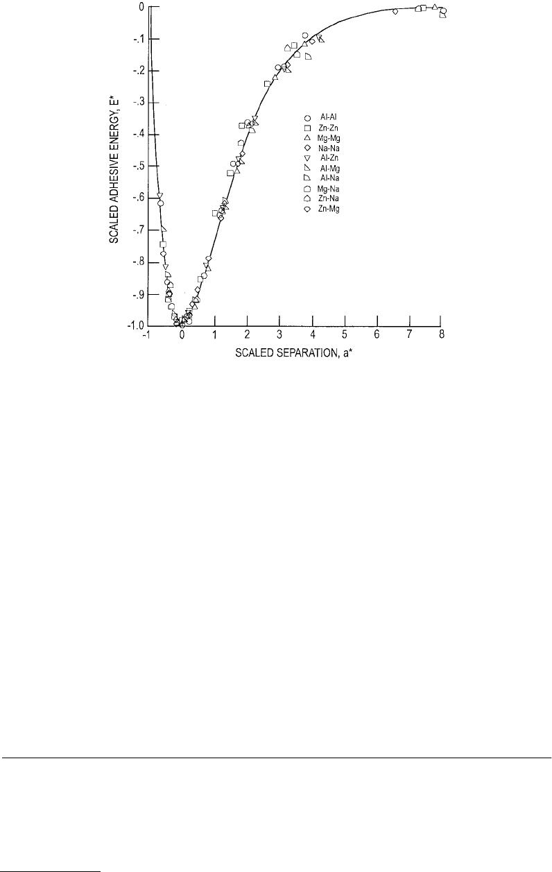
FIGURE 3.12
Scaled adhesive binding energy as a function of scaled separation for systems in Figure 3.11. (From
Rose, J.H. et al. (1983),
Phys. Rev. B
28, 1835–1845. With permission.)
© 1999 by CRC Press LLC
scattering (Niehus et al., 1993), low-energy backscattered electrons (De Crescenzi, 1995), and even sec-
ondary electron holography (Chambers, 1992), which we will not discuss. Other contributors to this
book address scanning probe microscopy and tribology, which are also nicely covered in an extensive
review article by Carpick and Salmeron (1997).
3.4.1 Low-Energy Electron Diffraction
Since LEED is a diffraction technique, when viewing a LEED pattern, you are viewing the reciprocal
lattice structure and not the atomic locations on the surface. A LEED pattern typically is obtained by
scattering a low-energy electron beam (0 to 300 eV) from a single-crystal surface in ultrahigh vacuum.
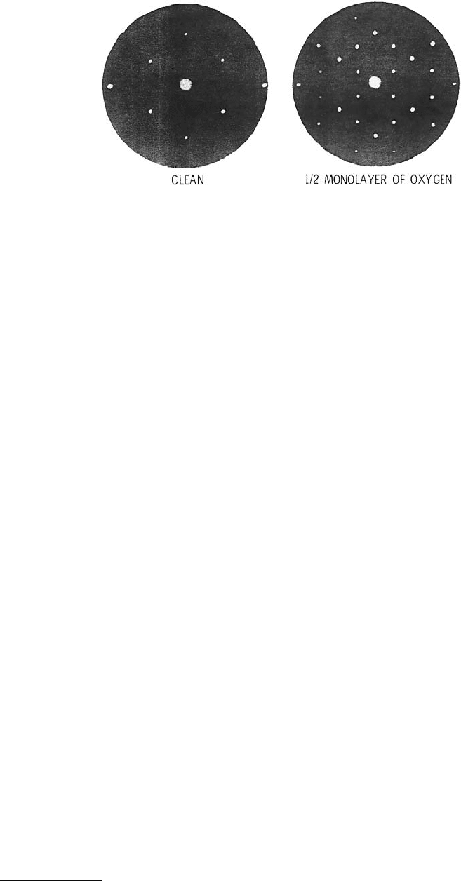
In Figure 3.13 we show the LEED pattern for the W(110) surface with a half monolayer of oxygen adsorbed
on it (Ferrante et al., 1973). We can first notice in Figure 3.13a that the pattern looks like the direct lattice
W(110) surface, but this only means that the diffraction pattern reflects the symmetry of the lattice.
Notice that in Figure 3.13b extra spots appear at
½
order positions upon adsorption of oxygen. Since
this is the reciprocal lattice, this means that the spacings of the rows of the chemisorbed oxygen actually
are at double the spacing of the underlying substrate. In fact, the interpretation of this pattern is more
complicated since the structure shown would not imply a
½
monolayer coverage, but is interpreted as
an overlapping of domains at 90° from one another. In this simple case the coverage is estimated by
adsorption experiments, where saturation is interpreted as a monolayer coverage. The interpretation of
patterns is further complicated, since with complex structures such as the silicon 7
×
7 pattern, the direct
lattice producing this reciprocal lattice is not unique. Therefore, it is necessary to have a method to select
between possible structures (Rous and Pendry, 1989).
We now digress for a moment in order to discuss the diffraction process. The most familiar reference
work is X-ray diffraction (Kittel, 1986). We know that for X rays the diffraction pattern of the bulk would
produce what is known as a Laue pattern where the spots represent reflections from different planes.
The standard diffraction condition for constructive interference of a wave reflected from successive planes
is given by the Bragg equation
(3.10)
where
d
is an interplanar spacing,
θ
is the diffraction angle,
λ
is the wavelength of the incident radiation,
and
n
is an integer indicating the order of diffraction. Only certain values of
θ
are allowed where
diffractions from different sets of parallel planes add up constructively. There is another simple method
for picturing the diffraction process known as the Ewald sphere construction (Kittel, 1986), where it can
be easily shown that the Bragg condition is equivalent to the relationship
FIGURE 3.13 LEED pattern for (a) clean and (b) oxidized tungsten (110) with one half monolayer of oxygen. The
incident electron beam energy for both patterns is 119 eV. (From Ferrante, J. et al. (1973), in Microanalysis Tools and
Techniques (McCall, J. L. and Mueller, W. M., eds.), Plenum Press, New York. With permission.)
2dnsin θλ=
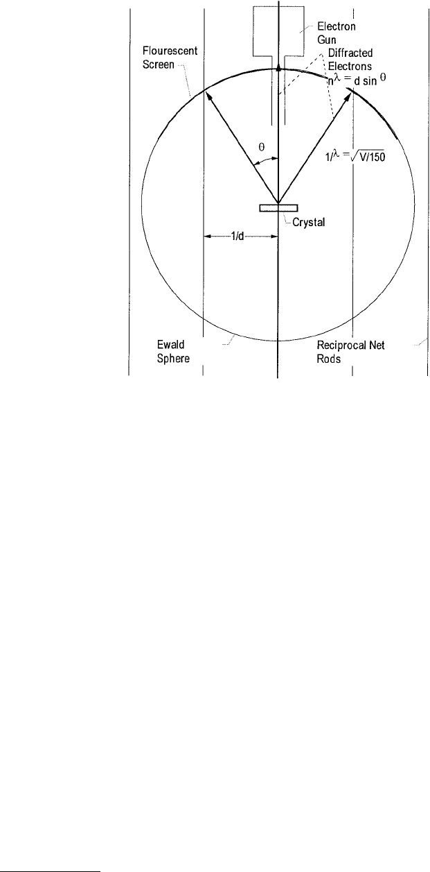
© 1999 by CRC Press LLC
(3.11)
where
→
k is the wave vector (2π/λ) of the incident beam,
→
k′ is the wave vector of the diffracted beam, and
→
G is a reciprocal lattice vector. The magnitude of the wave vectors k = k′ are equal since momentum is
conserved; i.e., we are only considering elastic scattering. Therefore, a sphere of radius k can be con-
structed, which when intersecting a reciprocal lattice point indicates a diffracted beam. This is equivalent
to the wave vector difference being equal to a reciprocal lattice vector, with that reciprocal lattice vector
normal to the set of planes of interest, and θ the angle between the wave vectors. In complex patterns,
spot intensities are used to distinguish between possible structures. The equivalent Ewald construction
for LEED is shown in Figure 3.14. We note that the reciprocal lattice for a true two-dimensional surface
would be a set of rods instead of a set of points. Consequently, the Ewald sphere will always intersect the
rods and give diffraction spots resulting from interferences due to scattering between rows of surface
atoms, with the number of spots changing with electron wavelength and incident angle. However, for
LEED complexity results from spot intensity modulation by the three-dimensional lattice structure, and
determining that direct lattice from the spot intensities. In X-ray diffraction the scattering is described
as kinematic, which means that only single scattering events are considered. With LEED, multiple
scattering occurs because of the low energy of the incident electrons; thus structure determination involves
solving a difficult quantum mechanics problem. Generally, various possible structures are constructed
and the multiple scattering problem is solved for each proposed structure. The structure that minimizes
the difference between the experimental intensity curves and the theoretical calculations is the probable
structure. There are a number of parameters involved with atomic positions and electronic properties,
and the best fit parameter is denoted as the “R-factor.” In spite of the seeming complexity, considerable
progress has been made and computer programs for performing the analysis are available (Van Hove
FIGURE 3.14 Ewald sphere construction for LEED. (From Ferrante, J. et al. (1973), in Microanalysis Tools and
Techniques (McCall, J. L., and Mueller, W. M., eds.), Plenum Press, New York. With permission.)
rr
r
kk G−
′
=

© 1999 by CRC Press LLC
et al., 1993). The LEED structures give valuable information about adsorbate binding which can be used
in the energy calculations described previously.
3.4.2 High-Resolution Electron Microscopy
Fundamentally, materials derive their properties from their makeup and structure, even down to the level
of the atomic ordering in alloys. To understand fully the behavior of materials as a function of their
composition, processing history, and structural characteristics, the highest resolution examination tools
are needed. In this section we will limit the discussion to electron microscopy techniques using commonly
available equipment and capable or achieving atomic-scale resolution. Traditional scanning electron
microscopy (SEM), therefore, will not be discussed, although in tribology SEM has been and should
continue to prove very useful, particularly when combined with X-ray spectroscopy. Many modern Auger
electron spectrometers (discussed in the next section on surface chemical analysis) also have high-
resolution scanning capabilities, and thus can perform imaging functions similar to a traditional SEM.
Another technique not discussed here is photoelectron emission microscopy (PEEM). While PEEM can
routinely image photoelectron yield (related to the work function) differences due to single atomic layers,
lateral resolution typically suffers in comparison to SEM. PEEM has been applied to tribological materials,
however, with interesting results (Montei and Kordesch, 1996).
Both transmission electron microscopy (TEM) and scanning transmission electron microscopy
(STEM) make use of an electron beam accelerated through a potential of, typically, up to a few hundred
thousand volts. Generically, the parts of a S/TEM consist of an electron source such as a hot filament or
field emission tip, a vacuum column down which the accelerated and collimated electrons are focused
by usually magnetic lenses, and an image collection section, often comprising a fluorescent screen for
immediate viewing combined with a film transport and exposure mechanism for recording images. The
sample is inserted directly into the beam column and must be electron transparent, both of which severely
limit sample size. There are numerous good texts available about just TEM and STEM (e.g., Hirsch et al.,
1977; Thomas and Goringe, 1979).
An advantage to probing a sample with high-energy electrons lies in the De Broglie formula relating
the motion of a particle to its wavelength
(3.12)
where λ is the electron wavelength, h is the Planck constant, m is the particle mass, and E
k
is the kinetic
energy of the particle. An electron accelerated through a 100-kV potential then has a wavelength of
0.04 Å, well below any diffraction limitation on atomic resolution imaging. This is in contrast with LEED,
for which electron wavelengths are typically of the same order as interatomic spacings. As the electron
beam energy increases in S/TEM, greater sample thickness can be penetrated with a usable signal reaching
the detector. Mitchell (1973) discusses the advantages of using very high accelerating voltages, which at
the time included TEM voltages up to 3 MV.
As the electron beam traverses a sample, any crystalline regions illuminated will diffract the beam,
forming patterns characteristic of the crystal type. Apertures in the microscope column allow the dif-
fraction patterns of selected sample areas to be observed. Electron diffraction patterns combined with
an ability to tilt the sample make determination of crystal type and orientation relatively easy, as discussed
in Section 4.1 above for X-ray Ewald sphere construction. Electrons traversing the sample can also
undergo an inelastic collision (losing energy), followed by coherent rescattering. This gives rise to cones
of radiation which reveal the symmetry of the reflecting crystal planes, showing up in diffraction images
as “Kikuchi lines,” named after the discoverer of the phenomenon. The geometry of the Kikuchi lines
provides a convenient way of determining crystal orientation with fairly high accuracy. Another technique
λ=
()
h
mE
k
2
12

© 1999 by CRC Press LLC
for illuminating sample orientation uses an aperture to select one of the diffracted beams to form the
image, which nicely highlights sample area from which that diffracted beam originates (“darkfield”
imaging technique).
One source of TEM image contrast is the electron beam interacting with crystal defects such as various
dislocations, stacking faults, or even strain around a small inclusion. How that contrast changes with
microscope settings can reveal information about the defect. For example, screw dislocations may “dis-
appear” (lose contrast) for specific relative orientations of crystal and electron beam. An additional tool
in examining the three-dimensional structures within a sample is stereomicroscopy, where two images
of the same area are captured tilted from one another, typically by around 10°. The two views are then
simultaneously shown each to one eye to reveal image feature depth.
For sample elemental composition, both an X-ray spectrometer and/or an electron energy-loss spec-
trometer can be added to the S/TEM. Particularly for STEM, due to minimal beam spreading during
passage through the sample the analyzed volume for either spectrometer can be as small as tens of
nanometers in diameter. X-ray and electron energy-loss spectrometers are somewhat complementary in
their ranges of easily detected elements. Characteristic X rays are more probable when exciting the heavier
elements, while electron energy losses due to light element K-shell excitations are easily resolvable.
Both TEM and STEM rely on transmission of an electron beam through the sample, placing an upper
limit on specimen thickness which depends on the accelerating voltage available and on specimen
composition. Samples are often thinned to less than a micrometer in thickness, with lateral dimensions
limited to a few millimeters. An inherent difficulty in S/TEM sample preparation thus is locating a given
region of interest within the region of visibility in the microscope, without altering sample characteristics
during any thinning process needed. For resolution at an atomic scale, columns of lighter element atoms
are needed for image contrast, so individual atoms are not “seen.” Samples also need to be somewhat
vacuum compatible, or at least stable enough in vacuum to allow examination. The electron beam itself
may alter the specimen by heating, by breaking down compounds within the sample, or by depositing
carbon on the sample surface if there are residual hydrocarbons in the microscope vacuum. In short,
S/TEM specimens should be robust under high-energy electron bombardment in vacuum.
3.4.3 Field Ion Microscopy
For many decades, FIM has provided direct lattice images from sharp metal tips. Some early efforts to
examine contact adhesion used the FIM tip as a model asperity, which was brought into contact with
various surfaces (Mueller and Nishikawa, 1968; Nishikawa and Mueller, 1968; Brainard and Buckley,
1971, 1973; Ferrante et al., 1973). As well, FIM has been applied to the study of friction (Tsukizoe et al.,
1985), the effect of adsorbed oxygen on adhesion (Ohmae et al., 1987), and even direct examination of
solid lubricants (Ohmae et al., 1990).
In FIM a sharp metal tip is biased to a high negative potential relative to a phosphor-coated screen in
an evacuated chamber backfilled to about a millitorr with helium or other noble gas. A helium atom
impinging on the tip experiences a high electric field due to the small tip radius. This field polarizes the
atom and creates a reasonable probability that an electron will tunnel from the atom to the metal tip
leaving behind a helium ion. Ionization is most probable directly over atoms in the tip where the local
radius of curvature is highest. Often, only 10 to 15% of the atoms on the tip located at the zone edges
and at kink sites are visible. The helium ions are then accelerated to a phosphorescent screen at some
distance from the tip, giving a large geometric magnification. Uncertainty in surface atom positions is
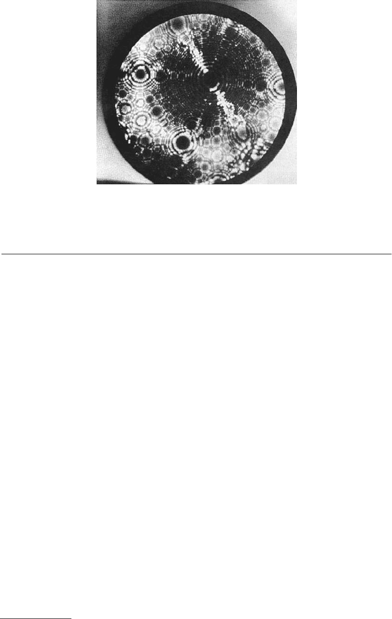
often reduced by cooling the tip to liquid helium temperature. Figure 3.15 is an FIM pattern for a clean
tungsten tip oriented in the (110) direction. The small rings are various crystallographic planes that
appear on a hemispherical single-crystal surface. A classic discussion of FIM pattern interpretation can
be found in Mueller (1969), a recent review has been published by Kellogg (1994), and a more extensive
discussion of FIM in tribology can be found in Ohmae (1993).
© 1999 by CRC Press LLC
3.5 Chemical Analysis of Surfaces
In this section we will discuss four of the many surface chemical analytic tools which we feel have had
the widest application in tribology, Auger electron spectroscopy (AES), X-ray photo-electron spectros-
copy (XPS), secondary ion mass spectroscopy (SIMS), and infrared spectroscopy (IRS). AES gives ele-
mental analysis of surfaces, but in some cases will give chemical compound information. XPS can give
compound information as well as elemental. SIMS can exhibit extreme elemental sensitivity as well as
“fingerprint” lubricant molecules. IR can identify hydrocarbons on surfaces, which is relevant because
most lubricants are hydrocarbon based. Hantsche (1989) gives a basic comparison of some surface analytic
techniques. Before launching into this discussion we wish to present a general discussion of surface
analyses. We use a process diagram to describe them given as
EXCITATION (INTERACTION)
⇓
DISPERSION
⇓
DETECTION
⇓
SPECTROGRAM
The first step, excitation in interaction, represents production of the particles or radiation to be
analyzed. In light or photon emission spectroscopy a spark causes the excitation of atoms to higher energy
states, thus emitting characteristic photons. The dispersion stage could be thought of as a filtering process
where the selected information is allowed to pass and other information is rejected. In light spectroscopy
this would correspond to the use of a grating or prism, for an ion or electron it might be an electrostatic
analyzer. Next is detection of the particle which could be a photographic plate for light or an electron
multiplier for ions or electrons. And, finally, the spectrogram tells what materials are present and, it is
hoped, how much is there.
FIGURE 3.15 Field ion microscope pattern of a clean tungsten tip oriented in the (110) direction. (From Ferrante,
J. et al. (1973), in Microanalysis Tools and Techniques ( McCall, J. L. and Mueller, W. M., eds.), Plenum, Press New
York. With permission.)
© 1999 by CRC Press LLC
3.5.1 Auger Electron Spectroscopy
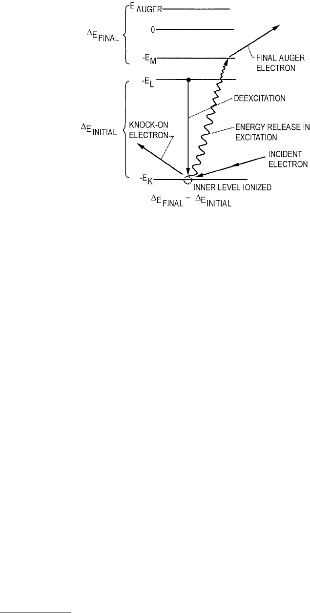
The physics of the Auger emission process is shown in Figure 3.16. An electron is accelerated to an energy
sufficient to ionize an inner level of an atom. In the relaxation process an electron drops into the ionized
energy level. The energy that is released from this de-excitation is absorbed by an electron in a higher
energy level, and if the energy is sufficient it will escape from the solid. The process shown is called a
KLM transition, i.e., a level in the K-shell is ionized, an electron decays from an L-shell, and the final
electron is emitted from an M-shell. Similarly, a process involving different levels will have corresponding
nomenclature. The energy of the emitted electron has a simple relationship to the energies of the levels
involved, depending only on differences between these levels. The relationships for the process shown are
(3.13)
giving
(3.14)
Consequently, since the energy levels of the atoms are generally known, the element can be identified.
There are surprisingly few overlaps for materials of interest. When peaks do overlap, other peaks peculiar
to the given element along with data manipulation can be used to deconvolute peaks close in energy.
AES will not detect hydrogen, helium, or atomic lithium because there are not enough electrons for the
process to occur. AES is surface sensitive because the energy of the escaping electrons is low enough they
cannot originate from very deep within the solid without detectable inelastic energy losses. The equipment
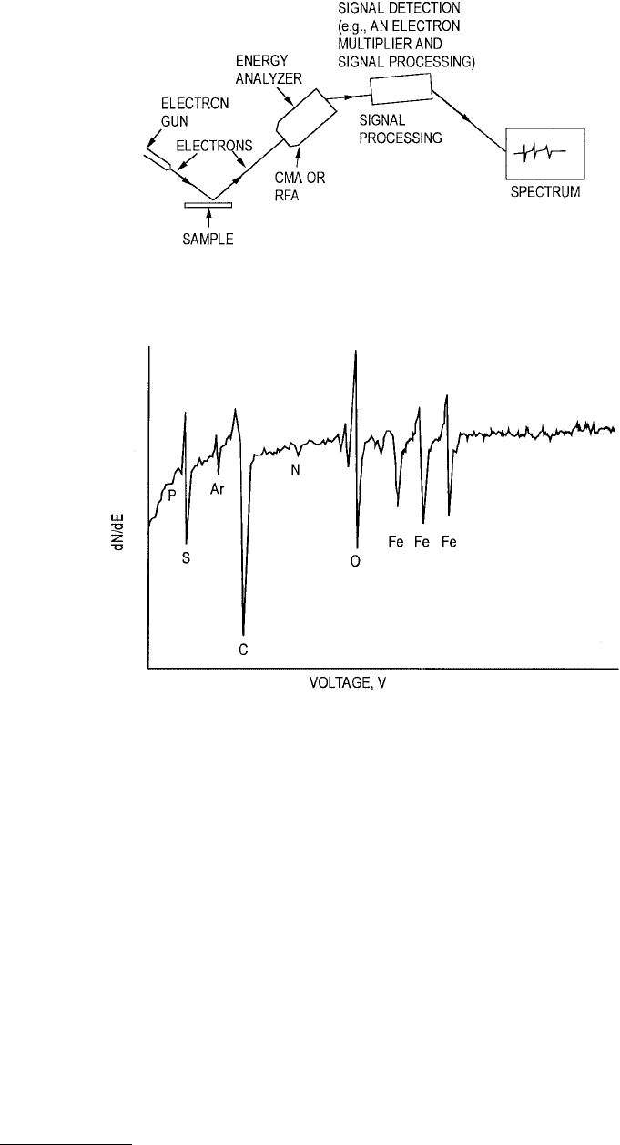
is shown schematically in Figure 3.17. The dispersion of the emitted electrons is usually accomplished
by any of a number of electrostatic analyzers, e.g., cylindrical mirror or hemispherical analyzers. Although
the operational details of the analyzers differ somewhat, the net result is the same.
An example spectrum is shown in Figure 3.18 for a wear scar on a pure iron pin worn with dibutyl
adipate with 1 wt. % zinc-dialkyl-dithiophosphate (ZDDP). This spectrum corresponds to the first
derivative of the actual spectral lines (peaks) in the spectrum (Brainard and Ferrante, 1979).
FIGURE 3.16 Auger transition diagram for an atom. (From Ferrante, J. et al. (1973), in Microanalysis Tools and
Techniques ( McCall J. L. and Mueller W. M., eds.), Plenum Press, New York. With permission.)
∆∆EE
final initial
=
EEEE
KLMAuger
=−−
© 1999 by CRC Press LLC
Historically, first-derivative spectra were taken because the actual peaks were very small compared
with the slowly varying background, posing signal-to-noise problems when amplification was sufficient
to bring out the peak. The derivative emphasized the more rapidly changing peak, but made quantification
more difficult, since the AES peaks are not a simple shape such as Gaussian, where a quantitative
relationship exists between the derivative peak-to-peak height and the area under the original peak. The
advent of dedicated microprocessors and the ability to digitize the results enable more-sophisticated
treatment of the data. The signal-to-background problem can now be handled by modeling the back-
ground and subtracting it, leaving an enhanced AES peak. Thus, the number of particles present can be
obtained by finding the area under the peak, enhancing the quantitative capability of AES. AES can be
chemically sensitive in that energy levels may shift when chemical reactions occur. Large shifts can be
detected in the AES spectrum, or alternatively peak shapes may change with chemical reaction. Some
examples of these effects will be given later in the chapter.
There are two other techniques that are used in conjunction with AES that should be mentioned,
scanning Auger microscopy (SAM) and depth profiling. SAM is simply “tuning” to a particular AES peak
and rastering the electron beam in order to obtain an elemental map of a surface. This can be particularly
FIGURE 3.17 Schematic diagram of AES apparatus. (From Ferrante, J. (1982), J. Am. Soc. Lubr. Eng. 38, 223–236.
With permission.)
FIGURE 3.18 Auger spectrum of wear scar on pure iron pin run against M2 tool steel disk in dibutyl adipate
containing 1 wt% ZDPP. Sliding speed, 2.5 cm/s; load, 4.9 N; atmosphere, dry air. (From Brainard, W. A. and Ferrante,
J. (1979), NASA TP-1544, Washington, D.C.)