Bhushan B. Handbook of Micro/Nano Tribology, Second Edition
Подождите немного. Документ загружается.

© 1999 by CRC Press LLC
the figure is curved with a slope of less than 1 shortly after the sample touches the tip, which suggests
that the tip has indented the sample. Later, the slope is equal to 1 suggesting that the tip no longer indents
the sample. This observation indicates that the tape surface is soft locally (polymer-rich) but it is hard
(as a result of magnetic particles) underneath. Since the curves in the extending and retracting modes
are identical, the indentation is elastic up to at a maximum load of about 22 nN used in the measurements.
A shown in Figure 14.48 for unlubricated and lubricated textured disks, the slope of the deflection
curves is 1 and remains constant as the disks touch and continue to push the AFM tip. The disks are not
indented.
14.6.2 Nanoscale Indentation
Nanoscale mechanical properties of magnetic media and single-crystal silicon have been measured by
Bhushan et al. (1994a–d, 1995a–e, 1997a, 1998) and Koinkar and Bhushan (1996a, 1997b). Bhushan et al.
(1994b) have reported that indentation hardness with a penetration depth as low as 1 nm can be measured
using AFM. Figures 14.49a and show the gray-scale plots and line plots of inverted images of indents
made on the as-received Si(111) at normal loads of 60, 65, 70, and 100 µN. Triangular indents can be
clearly observed with very shallow depths. It is found that below a normal load of 60 µN indents are
unobservable. At a normal load of 60 µN indents are observed and the depth of penetration is about
1 nm. As we increase the normal load, the indents become clearer and indentation depth increases.
Figure 14.50 shows a plot of hardness and normal load as a function of indentation depth. The indentation
depth increases with an increase in normal load. We note that the hardness at a small indentation depth
of 2.5 nm is 16.6 GPa and it drops to a value of 11.7 GPa at a depth of 7 nm and normal load of 100 µN.
The observed drop in the hardness values at higher loads (Figure 14.50) is comparable to the trends in
the nanohardness data measured using a commercial nanoindenter by Pharr et al. (1990) and Page et al.
(1992). Pharr et al. (1990) have reported a value of 11.4 GPa at large indentation depths (>50 nm) and
Page et al. (1992) have reported a value of about 14.2 GPa at an indentation depth of about 20 nm and
monotonic decrease in hardness to about 7.5 GPa at indentation depths of about 500 nm. Reported values
of microhardness values of silicon is about 9 to 10 GPa (Anonymous, 1988). If the silicon material is
used at very light loads such as in microsystems, the high hardness of surface films would protect the
surface until it is worn.
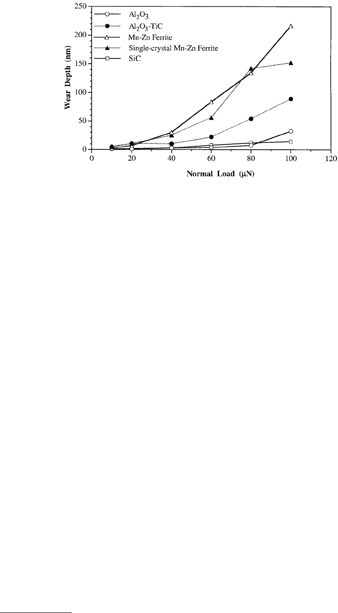
FIGURE 14.29 Wear depth as a function of normal load after one scan cycle for Al
2
O
3
, Al
2
O
3
–TiC, polycrystalline
Mn–Zn ferrite, single-crystal Mn–Zn ferrite, and SiC. (From Koinkar, V.N. and Bhushan, B., 1996, Wear 202, 110–122.
With permission.)

© 1999 by CRC Press LLC
Higher hardness values obtained in low-load indentation may arise from the observed pressure-
induced phase transformation during the nanoindentation (Pharr, 1991; Callahan and Morris, 1992).
Additional increase in the hardness at an even lower indentation depth of 2.5 nm reported here may arise
from the contribution by complex chemical films (not from native oxide films) present on the silicon
surface. At small volumes, there is a high probability that indentation would be made into a region that
was initially dislocation free. Furthermore, at small volumes, it is believed that there is an increase in the
stress necessary to operate dislocation sources (Gane and Cox, 1970; Sargent, 1986). These are some of
the plausible explanations for the increase in hardness at smaller volumes.
Nanohardness values of virgin, coated, and treated silicon samples are presented in Table 14.5. Coatings
and treatments improved nanohardness of silicon. We note that dry-oxidized and PECVD oxide films
are harder than wet-oxidized films, as these films may be porous (Bhushan and Venkatesan, 1993c). High
hardness of oxidized films may be responsible for lower wear and scratch resistance (Table 14.5). Hardness
values of virgin and C
+
-implanted Si(111) at various indentation depths (normal loads) are presented
in Figure 14.51. We note that the surface layer of the implanted zone is much harder than that of the
subsurface, and may be brittle leading to higher wear on the surface. Subsurface of the implanted zone
is harder than the virgin silicon, resulting in high wear resistance (data presented earlier, Figure 14.46).
Bhushan et al. (1994c) measured nanohardness of polished thin-film disks at loads of 80, 100, and
140 µN loads, Figure 14.52. Hardness values were 21 GPa (10 nm), 21 GPa (15 nm), and 9 GPa (40 nm);
the depths of indentation are shown in the parenthesis. The hardness value at 80 and 100 µN is much
higher than at 140 µN. This is expected since the indentation depth is only about 15 nm at 100 µN, which
is smaller than the thickness of DLC coating (~20 to 30 nm). The hardness value at lower loads is primarily
the value of the carbon coating. The hardness value at higher loads is primarily the value of the magnetic
film, which is softer than the carbon coating. This result is consistent with the scratch and wear data
discussed previously.
For the case of hardness measurements made on thin-film rigid disk at low loads, the indentation
depth is on the same order as the variation in the surface roughness. For accurate measurements of
indentation size and depth, it is desirable to subtract the original (unindented) profile from the indented
profile. Bhushan et al. (1994b,c, 1995d), and Lu and Bogy (1995) developed an algorithm for this purpose.
Because of hysteresis, a translational shift in the sample plane occurs during the scanning period, resulting
in a shift between images captured before and after indentation. Therefore, the image needs to be shifted
for perfect overlap before subtraction can be performed. For this purpose, a small region on the original
image was selected and the corresponding region in the indented image was found by maximizing the
correlation between the two regions. (Profiles were plane-fitted before subtraction.) Once two regions
were identified, overlapped areas between the two images were determined and the original image was
shifted with the required translational shift and then subtracted from the indented image. An example
of profiles before and after subtraction is shown in Figure 14.53. The indent on the subtracted image can
be measured easily. At a normal load of 140 µN the hardness value of polished, unlubricated magnetic
thin-film rigid disk (σ roughness = 3.3 nm) is 9.0 GPa and the indentation depth is 40 nm.
Figure 14.54a shows the hardness as a function of residual depth for three types of 100-nm-thick
amorphous carbon coatings deposited on silicon by sputtering, ion beam, and cathodic arc processes
(Kulkarni and Bhushan, 1997). Data on uncoated silicon are also included for comparisons. The cathodic
arc carbon coating exhibits highest hardness of about 24.9 GPa, whereas the sputtered and ion beam
carbon coatings exhibit hardness values of 17.2 and 15.2 GPa, respectively. The hardness of Si(100) is
13.2 GPa. High hardness of the cathodic arc carbon coating explains its high wear resistance, reported
earlier. Figure 14.54b shows the elastic modulus as a function of residual depth for various samples. The
cathodic arc coating exhibits the highest elastic modulus. Its elastic modulus decreases with an increasing
residual depth, while the elastic moduli for the other carbon coatings remain almost constant. In general,
hardness and elastic modulus of coatings are strongly influenced by their crystalline structure, stoichi-
ometry, and growth characteristics which depend on the deposition parameters. Mechanical properties
of carbon coatings have been known to change over a wide range with sp
3
–sp
2
bonding ratio and amount
© 1999 by CRC Press LLC

© 1999 by CRC Press LLC
of hydrogen. Hydrogen is believed to play an important role in the bonding configuration of carbon
atoms by helping to stabilize tetrahedral coordination of carbon atoms.
14.6.3 Localized Surface Elasticity
AFM can be used in the force modulation mode to measure surface elasticities in a nondestructive manner
(Maivald et al., 1991; DeVecchio and Bhushan, 1997; Scherer et al., 1997). By using this technique, it is
possible to measure quantitatively the elasticity of soft and compliant materials with penetration depths
of less than 100 nm. This technique has been successfully used to get localized elasticity maps of particulate
magnetic tapes. An elasticity map of a tape can be used to identify relative distribution of hard mag-
netic/nonmagnetic ceramic particles and the polymeric binder on the tape surface, which has an effect
on friction and stiction at the head-tape interface.
Figure 14.55 shows surface height and elasticity maps on a sample of metal particle magnetic tape.
The elasticity image reveals sharp variations in surface elasticity due to the composite nature of the film.
As can be clearly seen, regions of high elasticity do not always correspond to high or low topography.
Figure 14.56 shows measurements on three different formulations of magnetic tapes with a larger scan
size. It is seen that the number of stiff regions on the second two tapes is higher than that on the first
tape. The trend in increasing number of stiff regions has been correlated to reduced stiction problems
in these three tapes (Bhushan et al., 1997c). Based on a Hertzian elastic-contact analysis, the static
indentation depth of these samples during the force modulation scan is estimated to be about 1 nm. We
conclude that the contrast seen is influenced most strongly by material properties in the top few nanom-
eters, independent of the composite structure beneath the surface layer.
14.7 Detection of Material Transfer
Ruan and Bhushan (1993) conducted indentation on C
60
-rich fullerene films (Bhushan et al., 1993a,b)
using AFM in the force calibration mode. They observed transfer of fullerene molecules to the AFM tip
during indentation. The fullerene molecules transferred to the AFM tip were subsequently transported
to a diamond surface when the diamond sample was scanned with the contaminated tip, Figure 14.57.
The discontinuity in the tip deflection shown in Figure 14.57a is due to the transferred fullerene molecules
to the AFM tip. After repeated sliding of the tip against the diamond surface, the discontinuity in the tip
deflection disappeared as shown in Figure 14.57b. This demonstrates the capability of detection of
material transfer on a molecular scale using AFM.
14.8 Lubrication
The boundary films are formed by physical adsorption, chemical adsorption, and chemical reaction. The
physisorbed film can be either monomolecular or polymolecular thick. The chemisorbed films are
monomolecular, but stoichiometric films formed by chemical reaction can have a large film thickness.
In general, the stability and durability of surface films decrease in the following order: chemical reaction
films, chemisorbed films, and physisorbed films. A good boundary lubricant should have a high degree
of interaction between its molecules and the sliding surface. As a general rule, liquids are good lubricants
when they are polar and thus able to grip solid surfaces (or be adsorbed). Polar lubricants contain reactive
functional groups with low ionization potential or groups having high polarizability (Bhushan, 1993).
Boundary lubrication properties of lubricants are also dependent upon the molecular conformation and
lubricant spreading (Novotny et al., 1989; Novotny, 1990; Mate and Novotny, 1991; Mate, 1992a).
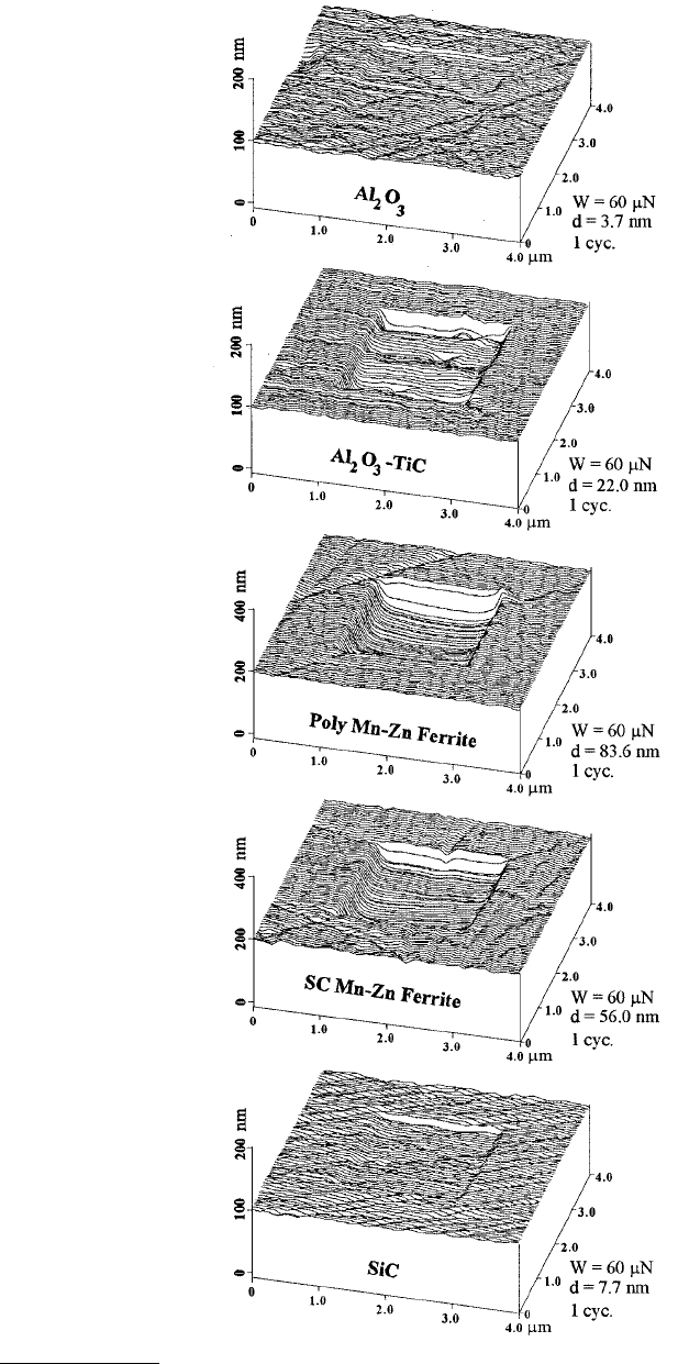
FIGURE 14.30 Surface profiles showing the worn region (center 2 × 2 µm) after one scan cycle at a normal load of
60 µN for Al
2
O
3
, Al
2
O
3
–TiC, polycrystalline Mn–Zn ferrite, single-crystal Mn–Zn ferrite, and SiC. (From Koinkar,
V.N. and Bhushan, B., 1996, Wear 202, 110–122. With permission.)
© 1999 by CRC Press LLC

© 1999 by CRC Press LLC
Mechanical interactions between the magnetic head and the medium in magnetic storage devices are
minimized by the lubrication of the magnetic medium. The primary function of the lubricant is to reduce
the wear of the medium and to ensure that friction remains low throughout the operation of the drive.
The main challenge, however, in selecting the best candidate for a specific surface is to find a material
that provides an acceptable wear protection for the entire life of the product, which can be several years
in duration. There are many requirements that a lubricant must satisfy in order to guarantee an acceptable
life performance. An optimum lubricant thickness is one of these requirements. If the lubricant film is
too thick, excessive stiction and mechanical failure of the head–disk is observed. On the other hand, if
the film is too thin, protection of the interface is compromised, and high friction and excessive wear will
result in catastrophic failure. An acceptable lubricant must exhibit properties such as chemical inertness,
low volatility, high thermal, oxidative and hydrolytic stability, shear stability, and good affinity to the
magnetic medium surface.
Fatty acid esters are excellent boundary lubricants, and esters such as tridecyl stearate, butyl stearate,
butyl palmitate, butyl myristate, stearic acid, and myrstic acid are commonly used as internal lubricants,
roughly 1 to 7% by weight of the magnetic coating in particulate flexible media (tapes and particulate
flexible disks). The fatty acids involved include those with acid groups with an even number of carbon
atoms between C
12
and C
22
, with alcohols ranging from C
3
to C
13
. These acids are all solids with melting
points above the normal surface operating temperature of the magnetic media. This suggests that the
decomposition products of the ester via lubrication chemistry during a head–flexible medium contact
may be the key to lubrication.
Topical lubrication is used to reduce the wear of rigid disks and thin-film tapes. Perfluoropolyethers
(PFPEs) are chemically the most stable lubricants with some boundary lubrication capability, and are
most commonly used for topical lubrication of rigid disks. PFPEs commonly used include Fomblin Z
and Fomblin Y lubricants, made by Ausimont, Milan, Italy; Krytox 143 AD, made by Dupont, U.S.; and
Demnum S, made by Diakin, Japan; and their difunctional derivatives containing various reactive end
groups e.g., hydroxyl or alcohol (Fomblin Z-Dol), piperonyl (Fomblin AM 2001), isocyanate (Fomblin
Z-Disoc), and ester (Demnum SP). The difunctional derivatives are referred to as reactive (polar) PFPE
lubricants. The chemical structures, molecular weights, and viscosities of various types of PFPE lubricants
are given in Table 14.6. We note that rheological properties of thin films of lubricants are expected to be
different from their bulk properties. Fomblin Z and Demnum S are linear PFPE, and Fomblin Y and
Krytox 143 AD are branched PFPE, where the regularity of the chain is perturbed by –CF
3
side groups.
The bulk viscosity of Fomblin Y and Krytox 143 AD is almost an order of magnitude higher than the
Z-type. Fomblin Z is thermally decomposed more rapidly than Y (Bhushan, 1993). The molecular
diameter is about 0.8 nm for these lubricant molecules. The monolayer thickness of these molecules
depends on the molecular conformations of the polymer chain on the surface (Novotny et al., 1989; Mate
and Novotny, 1991).
The adsorption of the lubricant molecules on a magnetic disk surface is due to van der Waals forces,
which are too weak to offset the spin-off losses, or to arrest displacement of the lubricant by water or
other ambient contaminants. Considering that these lubricating films are on the order of a monolayer
thick and are required to function satisfactorily for the duration of several years, the task of developing
a workable interface is quite formidable. An approach aiming at alleviating these shortcomings is to
enhance the attachment of the molecules to the overcoat, which, for most cases, is sputtered carbon.
There are basically two approaches which have been shown to be successful in bonding the monolayer
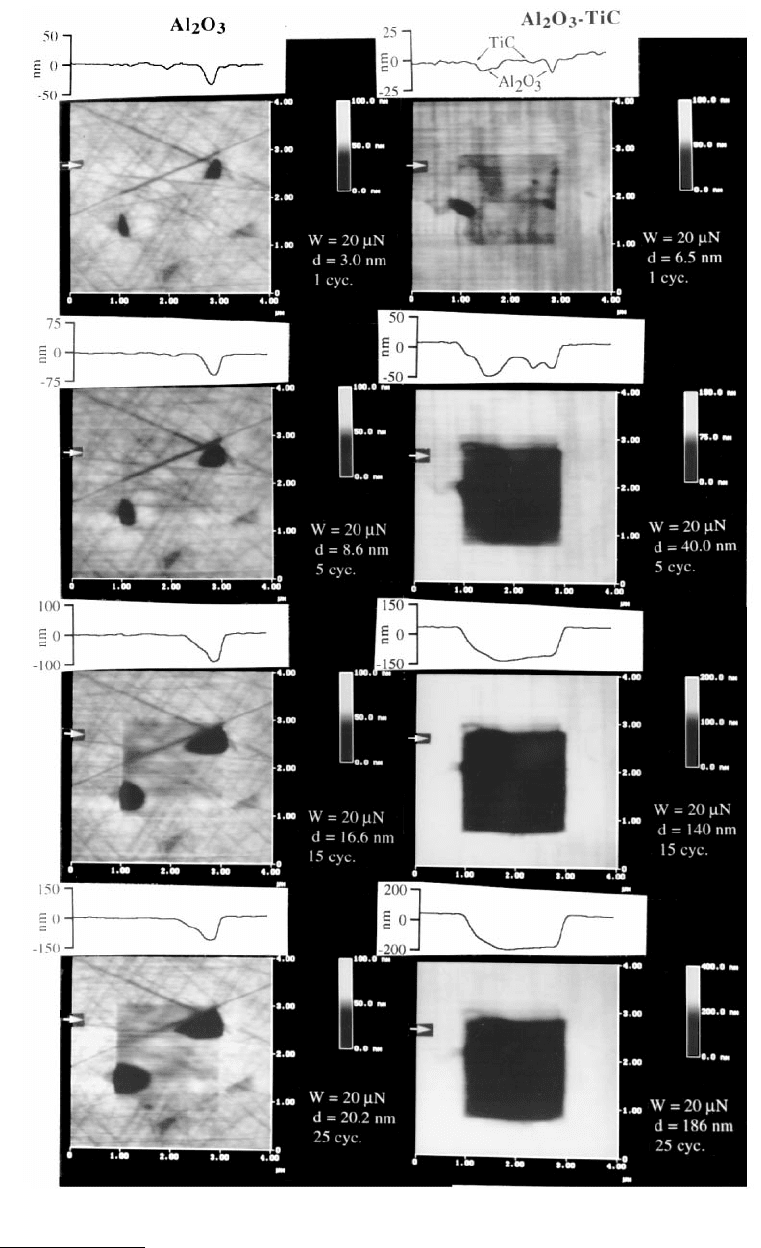
FIGURE 14.31 Gray-scale two-dimensional plots showing the worn region (center 2 × 2 µm) at a normal load of
20 µN and different number of scan cycles for Al
2
O
3
and Al
2
O
3
–TiC. The two-dimensional section plots taken at a
location shown by an arrow are shown on the top of corresponding gray-scale plot. Note the change in vertical scale
for gray-scale and two-dimensional section plots. (From Koinkar, V.N. and Bhushan, B., 1996, Wear 202, 110–122.
With permission.)
© 1999 by CRC Press LLC
to the carbon. The first relies on exposure of the disk lubricated with neutral PFPE to various forms of
radiation, such as low-energy X ray (Heidemann and Wirth, 1984), nitrogen plasma (Homola et al.,
1990), or far ultraviolet (e.g., 185 nm) (Saperstein and Lin, 1990). Another approach is to use chemically
active PFPE molecules, where the various functional (reactive) end groups offer the opportunity of strong
attachments to specific interface. These functional groups can react with surfaces and bond the lubricant
to the disk surface, which reduces its loss due to spin off and evaporation. Bonding of lubricant to the
disk surface depends upon the surface cleanliness. After lubrication, the disk is generally heated at 150°C
for 30 min to 1 h to improve the bonding. If only a bonded lubrication is desired, the unbonded fraction
can be removed by washing it off for 60 s with a nonfreon solvent (FC-72). Their main advantage is their
ability to enhance durability without the problem of stiction usually associated with weakly bonded
lubricants (Bhushan, 1996a).
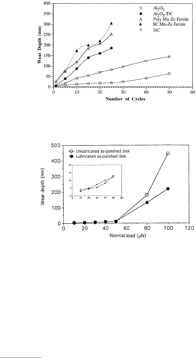
FIGURE 14.32 Wear depth as a function of number of cycles at a normal load of 20 µN for Al
2
O
3
, Al
2
O
3
–TiC,
polycrystalline Mn–Zn ferrite, single-crystal (SC) Mn–Zn ferrite, and SiC. (From Koinkar, V.N. and Bhushan, B.,
1996, Wear 202, 110–122. With permission.)
FIGURE 14.33 Wear depth as a function of normal load for polished, lubricated and unlubricated thin-film rigid
disks after one cycle. (From Bhushan, B. et al., 1994, Proc. Inst. Mech. Eng. Part J: J. Eng. Tribol. 208, 17–29. With
permission.)
© 1999 by CRC Press LLC
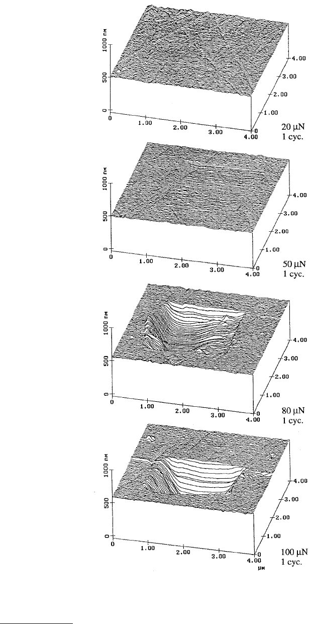
FIGURE 14.34 Surface maps of a polished, unlubricated thin-film rigid disk showing the worn region (center 2 ×
2 µm) after one cycle. The normal loads are indicated in the figure. (From Bhushan, B. et al., 1994, Proc. Inst. Mech.
Eng. Part J: J. Eng. Tribol. 208, 17–29. With permission.)
© 1999 by CRC Press LLC
Fomblin Y and Z are most commonly used for lubrication of particulate and thin-film rigid disks,
respectively. Lubricants with lower viscosity (such as Fomblin Z-types) with polar end groups (Z-Dol
and AM 2001) are most commonly used in thin-film disks in order to minimize stiction.
14.8.1 Imaging of Lubricant Molecules
Kaneko et al. (1991b) and Andoh et al. (1992) used scanning tunneling microscope (STM) to observe
the configuration, adsorption, and mobility of perfluoropolyether lubricants on HOPG (defect-free and
inactive surface), MoS
2
, and sputtered carbon (active surface). (Also see Foster and Frommer, 1988.)
Their study revealed that the lubricant molecules can easily change position and are mobile. They found
that adsorption of the lubricant molecules on a sputtered carbon surface is more than that on the HOPG.
14.8.2 Measurement of Localized Lubricant Film Thickness
The local lubricant thickness is measured by Fourier transform infrared spectroscopy (FTIR), ellipsom-
etry, angle-resolved X-ray photon spectroscopy (XPS), STM, and AFM. Ellipsometry and angle-resolved
XPS have excellent vertical resolution, on the order of 0.1 nm, but their lateral resolutions are on the
order of 1 and 0.2 mm, respectively. AFM can measure the thickness of the liquid film with a lateral
resolution on the order of the tip radius, about 100 nm, which it is not possible to achieve by other
techniques (Bhushan, 1993).
The schematic of AFM used for measurement for localized lubricant-film thickness by Mate et al.
(Mate et al., 1989, 1990; Bhushan and Blackman, 1991) is shown in Figure 14.58. The lubricant thickness
is obtained by measuring the forces on the tip as it approaches, contacts, and pushes through the liquid
film. In the left part of Figure 14.58 is a diagram of an AFM tip interacting with a lubricant-covered
particulate rigid disk. A typical force-vs.-distance curve for a tungsten tip of radius ~100 nm dipped into
a disk surface coated with a perfluoropolyether lubricant is shown in Figure 14.59. As the surface
approaches the tip, the liquid wicks up, causing a sharp onset of attractive force. The so-called meniscus
force experienced by the tip is ~4πRγ, where R is the radius of the tip and γ is the surface tension of the
liquid. In Figure 14.59, the attractive force measured is about 5 × 10
-8
N. While in the liquid film, the
forces on the lever remain constant until repulsive contact with the disk surface occurs. The distance
between the sharp snap-in at the liquid surface and the hard wall of the substrate is proportional to the
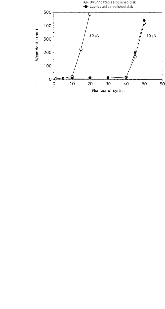
FIGURE 14.35 Wear depth as a function of number of cycles for polished, lubricated, and unlubricated thin-film
rigid disks at 10 µN and for polished, unlubricated disk at 20 µN. (From Bhushan, B. et al., 1994, Proc. Inst. Mech.
Eng. Part J: J. Eng. Tribol. 208, 17–29. With permission.)
© 1999 by CRC Press LLC
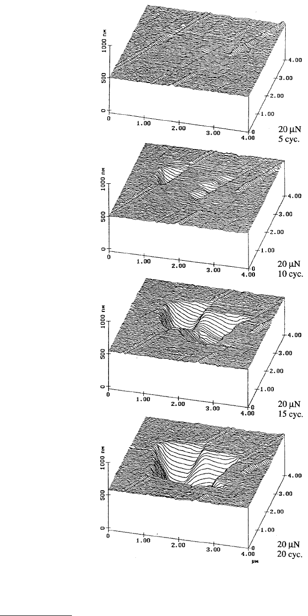
FIGURE 14.36 Surface maps of a polished, unlubricated thin-film rigid disk showing the worn region (center 2 ×
2 µm) at 20 µN. The number of cycles are indicated in the figure. (From Bhushan, B. et al., 1994, Proc. Inst. Mech.
Eng. Part J: J. Eng. Tribol. 208, 17–29. With permission.)