Bowker M., Davies P.R. (Eds.) Scanning Tunneling Microscopy in Surface Science, Nanoscience and Catalysis
Подождите немного. Документ загружается.

5.2.2
Technical Realization
While the first STM studies of electrode surfaces were performed with self-built
instruments, scanning tunneling microscopes for electrochemical use are nowadays
commercially available at a price that hardly justifies the effort of homemade
equipment. Nevertheless, new instrumental designs are now and then discussed
in the literature, which are still worthwhile to be considered for special applications.
There is, however, additional equipment required for the operation of an electro-
chemical STM, for which homemade designs may be advantageous over commer-
cially available ones and hence is briefl y mentioned here in terms of tip preparation
and isolation, the electrochemical cell, and vibration damping.
5.2.2.1 Tip Preparation and Isolation
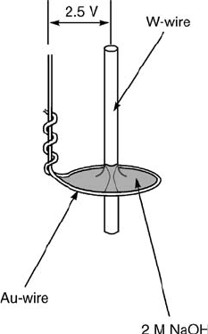
Very fine tips are required for high lateral resolution. The most commonly used tip
materials are tungsten and a platinum–iridium alloy (80 : 20). Tips are manufactured
by electrochemical etching of a 0.25 mm thick wire in a lamella of solution
(Figure 5.5) [21]. For W tips, the solution consists of 2 M NaOH (etching at 2.4 V
DC), for Pt:Ir tips 3.4 M NaCN is used (and 4.2 V AC). For tungsten, both parts can be
used as tips, while with Pt:Ir only the lower part is suitable for high-quality imaging.
While from an electrochemical point of view, Pt:Ir tips are easier to handle, their
potential range of stability being clearly larger than that for tungsten, W tips are
sharper and yield better images. Atomically resolved images are preferably obtained
from tungsten tips. We mention in passing that according to literature, Pt:Ir tips
were frequently produced by simply cutting the wire with a pair of pliers, with
reasonably good success as far as imaging is concerned. According to our experience,
tips produced in this way are not very suitable for electrochemical studies, but we
have used such tips for imaging surfaces in air. It seems important to cut the wire
while it is being pulled.
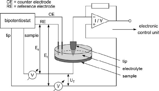
Figure 5.4 Electric circuit for in situ STM, which allowssample and
tip potentials to be controlled independent from each other.
124
j
5 Characterization and Modification of Electrode Surfaces by In Situ STM
For in situ STM measurements, the tip is inevitably immersed into the electrolyte
and acts as a fourth electrode with reactions occurring at the tip–electrolyte interface.
To reduce the electrochemical current at the tip to a size well below the tunnel
current at the tip, the area in contact with the solution must be reduced by coating the
largest portion of the STM tip with an insulating layer. In the literature, various ways
of insulating the tip have been described. In the past, Apiezon
, a chemically very
inert thermoplast, has been used with success [22, 23], but at present, electrophoretic
paints are widely employed for tip insulation [24]. In both cases, the uncoated part of
the tip is about 1 mm or less, leaving an area in contact with solution of the order of
10
8
–10
7
cm
2
. The remaining electrochemical currents are generally smaller than
50 pA (which is below the detection limit of commercial STM potentiostats), and they
no longer interfere with the imaging process. Besides the reduction of the electro-
chemically active area of the tip, the proper choice of the tip potential can also help in
minimizing Faradaic currents through the tip/electrolyte interface. This requires the
use of a bipotentiostat, which allows one to choose the tip potential independent
of the sample potential with respect to a common reference electrode. Such a
bipotentiostat is supplied by most STM manufacturers. It enables one to select a tip
potential close to the rest potential of the tip, where by definition no Faradaic currents
should flow. While this precaution was indeed necessary a few years ago, the tip
insulation has meanwhile progressed to a point, where restrictions of the tip
potential to values close to the rest potential are no longer necessary. This has been
an important advancement because with a freely chosen tip potential, scanning
tunneling spectroscopy becomes feasible, albeit in a very limited potential region
dictated by the decomposition of water or the stability of the tip material against
anodic oxidation.
Figure 5.5 Setup for the tip production by electrochemical etching
of a tungsten wire. (Reproduced with permission from Ref. [21].)
5.2 In Situ STM: Principle, Technical Realization and Limitations
j
125
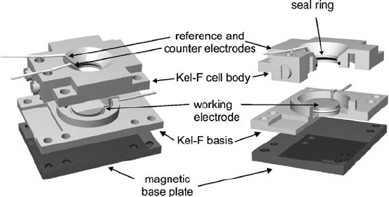
5.2.2.2 Electrochemical Cell
The design of the electrochemical cell is largely determined by (a) the shape of the
single-crystal electrodes to be studied and (b) the stringent requirements for a
thorough cleaning before its use. The design of our electrochemical STM cells is
shown in Figure 5.6. All parts are made of Kel-F, which is easy to clean and which
resists strongly oxidizing agents, such as caroic acid (conc. H
2
SO
4
þ 30% H
2
O
2
),
and the cell is designed for single-crystal disks of about 10 mm diameter and 2 mm
thickness. Since only the polished face of the single-crystal disk is in contact with
the electrolyte, electrochemical experiments can in principle be performed in the
STM cell, for example, for surface characterization by cyclic voltammetry. However,
one has to keep in mind that the cell has been optimized for STM use rather than for
electrochemical experiments and accordingly two major deficiencies prevent one
from obtaining high-quality cyclic voltammograms, routinely recorded in normal
electrochemical cells: (a) the STM cell is usually open to air, hence oxygen reduction
distorts the current–potential curves and (b) it normally takes minutes to assemble
the STM cell, which creates contamination problems. Consequently in most cases,
STM images and the corresponding electrochemical characterization are obtained
in different cells and different experiments.
The electrolyte volume of the STM cells is usually very small (of the order of a 100 ml
in the above-described case) and evaporation of the solution can create problems in
long-term experiments. Miniature reference electrodes, mostly saturated calomel
electrodes (SCE), have been described in the literature [25], although they are hardly
used anymore in our laboratory for practical reasons: Cleaning the glassware in caroic
acid becomes cumbersome. For most studies, a simple Pt wire, immersed directly
into solution, is a convenient, low-noise quasireference electrode. The Pt wire is
readily cleaned by holding it into a Bunsen flame, and it provides a fairly constant
reference potential of E
Pt
¼þ0.55 0.05 V versus SCE for 0.1 M sulfuric or per-
chloric acid solutions ( þ0.67 0.05 V for 0.1 M nitric acid), which has to be checked
from time to time and for different solutions.
Figure 5.6 Electrochemical cell design as used in the authors laboratory for STM.
126
j
5 Characterization and Modification of Electrode Surfaces by In Situ STM
5.2.2.3 Vibration Damping
It is obvious from the principle of STM that the microscope has to be shielded from
mechanical and acoustic vibrations of the outside world as much as possibleto achieve
good imaging quality, particularly if atomic resolution is required. After all, there are
two macroscopic parts – tip and sample – that are only fractions of a nanometer apart,
and this distanceneedsto becontrolled within hundredths ofa nanometer. Experience
has shown that vibrations of the building with frequencies below 10 Hz are especially
critical, that is, difficult to eliminate. A simple, yet very effective construction for
vibration damping is described in Ref. [26]. It consists in essence of two platforms, a
very heavy stone plate (about 200 kg) and a light one (e.g., a wooden board, onto which
the STM rests), suspended on metal frames with springs that have vastly different
forceconstants [27]. Needlessto saythat thepreferred locationfor settingup an STMis
the basement rather than the top floor ofa building. The microscopeis placed in a little
Faraday cage, lined with foam rubber for damping acoustic waves.
5.2.3
Limitations
Possible limitations in the use of STM arise from the close proximity of the tip to that
part of the sample that is imaged. Under normal imaging conditions, for example,
I
T
¼2 nA and U
T
¼50 mV,the tip–substrate distance s can beestimated from Eq. (5.1)
to be around 0.6 nm (with f
T
¼1.5 eV [15]). Considering the fact that the electric
double layer of a metal electrode in concentrated solution is about 0.3 nm thick [28,
29], the double layers of tip and substrate begin to merge and the ideal picture of
a noninteracting tip is no longer valid under these conditions. For example, contact
with the reference electrode for the imaged area right underneath the tip may be lost
because the bulk electrolyte that carries the reference potential has been squeezed
out. It has been shown that a Cu surface can be locally corroded right underneath the
tip if a positive potential is applied to the tip rather than to the sample [30]. Another
disturbance brought about the STM tip is the so-called tip shielding [31]. Considering
a typical tip radius of a few tens of nanometers, tip and sample constitute an extreme
example of a thin-layer cell with restricted diffusion of reactants to the imaged area
(e.g., metal ions in metal deposition studies) and with iR-drops distorting the
externally applied electrode potential. Hence, great care must be exercised when
treating kinetic data acquired by an STM as absolute; the mere presence of the tip
under tunneling conditions can strongly affect the kinetics of a reaction.
Finally, some requirements with respect to the substrates under study should be
mentioned. One may notice that practically all STM studies are performed with
single-crystal electrodes and not with (industrially more relevant) polycrystalline
samples. For one, this certainly has something to do with the high lateral resolution
that the STM offers and the researcher wants to make use of. Rough surfaces
would be too demanding for a feedback circuit, capable of reacting to atomic heights.
Since mechanistic interpretations of electrochemical reactions require well-defined
surface structures and atomically resolved images of bare and adsorbate-covered
5.2 In Situ STM: Principle, Technical Realization and Limitations
j
127
electrodes, one has to retreat to single-crystal electrodes. However, the STM-derived
structure information stems from a tiny area of the electrode, typically 100 nm 100
nm, and needs to be compared with electrochemical data that inevitably represent
the whole macroscopic electrode surface. Such a relation will be meaningful only if
the structure information holds for the whole electrode surface. This is the case only
for high-quality single-crystal surfaces.
5.3
Imaging Single-Crystal Surfaces of Catalytically Relevant Systems
5.3.1
Preparation and Imaging of Metal Single-Crystal Surfaces
Mechanistic interpretations of electrochemical processes, which involve adsorption
of reaction intermediates or products, require in general the use of single-crystal
electrodes with structurally well-defined surfaces. Classical examples are the oxida-
tion of small organic molecules such as formic acid [32] or the underpotential
deposition of metals [33, 34]. In the 1970s, right at the beginning of electrochemical
surface science, single-crystal surfaces were prepared in a UHV chamber by
sputtering and annealing, and their structure and cleanliness checked by electron
diffraction and AES [35–37]. This was a rather cumbersome approach for electro-
chemists and limited the use of well-characterized electrodes to those groups that
had access to surface science equipment. A significant advancement of single-crystal
electrochemistry came with the so-called flame-annealing technique, which required
in essence only a Bunsen burner to prepare clean and well-ordered surfaces, as first
demonstrated by Clavilier et al. for platinum [38] and later by Hamelin for gold [39].
Although the initial advice of the French school, to quench rapidly the still hot crystal
in water to reduce the danger of surface contamination as much as possible, had
to be abandoned because the heat shock turned out to be detrimental to the bulk
crystallinity, the resulting surface quality in retrospect has to be considered high. For
platinum, which is particularly sensitive to contamination from air, cooling in an
iodine [40] or CO [41] atmosphere was advocated, the adsorbed layer protecting the
surface extremely well during transfer to the electrochemical cell and being finally
removed from the surface by oxidative desorption. Ultimately, inductive heating in
a reducing atmosphere turned out to be the best choice as this technique allows the
preparation of clean and well-ordered surfaces of reactive metals such as Cu, Ag, Pd,
Rh, and Ru for which the by now classical flame-annealing in ambient atmosphere
has failed. This is particularly true for large single-crystal electrodes, commonly
employed for spectroscopic studies, which due to their higher heat capacity require
longer cooling times. Details of the technique can be found in Ref. [42]; a schematic
diagram is given in Figure 5.7.
The devastating influence of trace amounts of oxygen during cooling on the quality
of a Pt single-crystal surface is demonstrated in Figure 5.8, where the STM images
of Pt(1 1 1) in 0.1 M H
2
SO
4
after cooling down the crystal in air and in hydrogen
128
j
5 Characterization and Modification of Electrode Surfaces by In Situ STM
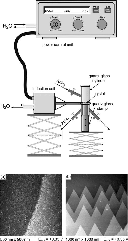
Figure 5.7 Setup for the inductive heating of single-crystal electrodes in controlled atmosphere.
Figure 5.8 STM images of Pt(1 1 1) in 0.1 M H
2
SO
4
at þ0.35 V
versus SCE, after cooling the sample in air (a) and in H
2
(b).
(Reproduced with permission from L.A. Kibler, personal
communication.)
5.3 Imaging Single-Crystal Surfaces of Catalytically Relevant Systems
j
129
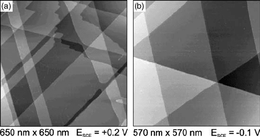
are compared (L.A. Kibler, personal communication). While cooling in air leads to a
rough surface, cooling in a reducing atmosphere such as H
2
or H
2
/Ar mixtures yields
large, atomically flat terraces. Other examples of well-prepared single-crystal surfaces
are given in Figure 5.9, which shows Pd(1 1 1) and Rh(1 1 1) in 0.1 M H
2
SO
4
[43].
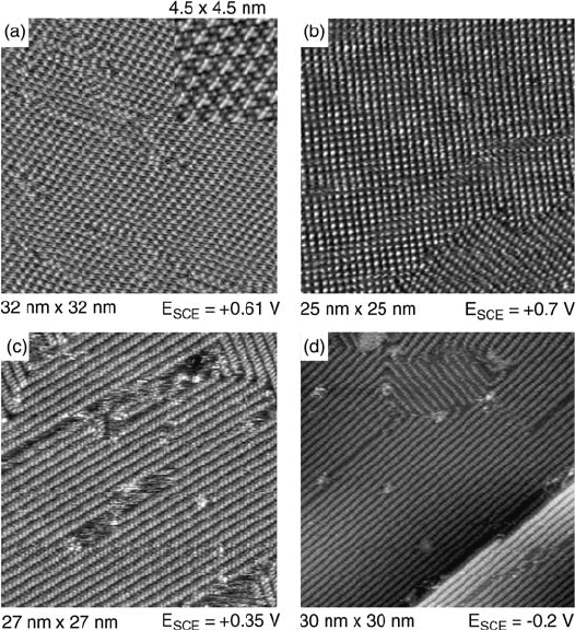
Quite often atomically resolved in situ images of single-crystal surfaces are
desirable because they would allow a precise length calibration of the piezos.
However, zooming with the microscope into the terraces, one frequently images
anion adlayers rather than the metal surface proper. Although interesting in their
own right, these adlayers prevent direct viewing of the substrate. Sulfate, chloride,
and metal chloro complexes are well known to form ordered adlayers [44], at least
at high coverages, which are easy to image by STM with molecular resolution.
Examples thereof are given in Figure 5.10 [45–48].
5.3.2
Bimetallic Surfaces
Bimetallic surfaces, either alloys or a metal A onto which a metal B was deposited
in submonolayer amounts, play an important role in electrocatalysis. For their
structural characterization, a chemical contrast in the STM images would be highly
desirable. So far, however, the number of such examples is vanishingly small, and
in almost all cases, one has to rely on morphological (height) contrast. A rare example
of a system showing chemical contrast is Pd and Au as has been demonstrated for
Pd deposits on Au(1 1 1) [49] as well as for Pd–Au alloy surfaces [50]. When Pd is
deposited from aqueous solution onto Au(1 1 1), nucleation starts exclusively at the
monoatomic high steps of the substrate, followed by a two-dimensional growth of
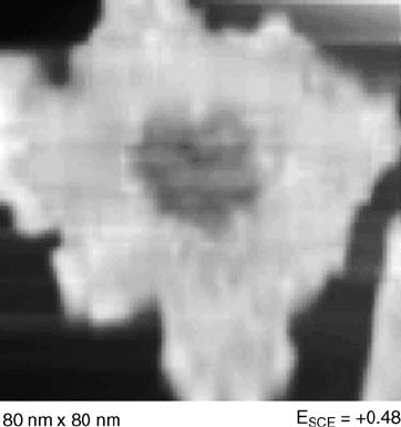
the Pd onto the lower terrace. Figure 5.11 shows the growth of a Pd layer that had
nucleated at the rim of a monoatomic high gold island. Although the monolayers of
both metals should have about the same height (the Pd layer being slightly lower, if
at all), the gold island appears darker in the STM image than the surrounding Pd.
Figure 5.9 STM images of (a) Pd(1 1 1) in 0.01 M H
2
SO
4
and (b)
Rh(111)in0.1 MH
2
SO
4
.BothcrystalswereannealedinaH
2
-flame
and cooled in H
2
. (Reproduced with permission from Ref. [43].)
130
j
5 Characterization and Modification of Electrode Surfaces by In Situ STM
This chemical contrast may be due to electronic effects or caused by differences in
anion adsorption on both metals. Evidence for electronic effects as possible origin of
the chemical contrast between Pd and Au has been presented in STM images of
Pd/Au alloy surfaces with atomic resolution, which allowed an identification of Pd or
Au atoms on the basis of their brightness [50]. A similar picture is presented in
Figure 5.12 showing the surface of a Pt
50
Ru
50
alloy [43]. There are atoms that appear
clearly brighter (about 0.04 nm higher), which in accordance with UHV–STM
investigations [51, 52] could be assigned to Ru because of its higher electron density
at the Fermi level. Their number, however, is much smaller than that of the Pt atoms,
indicating a marked difference between bulk and surface composition of the alloy.
Indeed, the corresponding cyclic voltammograms recorded in 0.1 M H
2
SO
4
reveals
a surface that is almost Pt(1 1 1)-like. From the image in Figure 5.12 it is concluded
that the Ru atoms are more or less uniformly distributed over the surface and only
small assemblies are formed. Wemention in passing that cooling the Pt
50
Ru
50
single-
crystal alloy after inductive heating in a reducing atmosphere yields the Pt-rich
Figure 5.10 STM images of ordered anionic adlayers. (a) PdCl
4
2
on Au(1 0 0) in 0.1 M H
2
SO
4
þ 0.1 mM H
2
PdCl
4
þ 0.6 mM
HCl [45]; (b) PtCl
4
2
on Au(1 0 0) in 0.1 M H
2
SO
4
þ 0.1 mM
K
2
PtCl
4
[46]; (c) sulfate on Au(1 0 0) in 0.1 M H
2
SO
4
[47];
(d) sulfate on Ag(1 0 0) in 0.1 M H
2
SO
4
[48].
5.3 Imaging Single-Crystal Surfaces of Catalytically Relevant Systems
j
131
surface, whereas cooling in an inert (Ar) atmosphere with traces of oxygen leads to a
Ru-rich surface [53, 54].
From the image in Figure 5.12 one may guess how difficult the measurements and
how limited the systems are that show a true chemical contrast. In most cases, one
has to retreat to the morphological information in order to assign features to metal A
or metal B. This is routinely done in metal deposition studies that start with an image
of the bare surface, followed by the ones with the metal deposit at various stages,
that is, various amounts. Numerous examples are given in the literature [26, 55, 56],
one being reproduced in Figure 5.13. It shows Pt electrodeposited onto Au(1 1 1),
the little hillocks on a flat substrate being easily identified as the Pt clusters [46]. With
this image another well-established observation is confirmed: Nucleation starts
preferentially at surface defects, the growing nuclei decorating the substrates defect
structure.
5.4
Strategies for Nanostructuring Surfaces
5.4.1
Oxidation–Reduction Cycles for Roughening and Faceting Surfaces
The dominance of surface defects over terrace sites in catalysis and electrocatalysis
had been recognized already in the early stages of surface science. For example,
Figure 5.11 STM image of a growing Pd monolayer, which had
nucleated on Au(1 1 1) at the rim of a gold island. Although
practically equal in height, the Pd layer appears brighter than the
gold island in the center. (Reproduced with permission from
Ref. [49].)
132
j
5 Characterization and Modification of Electrode Surfaces by In Situ STM
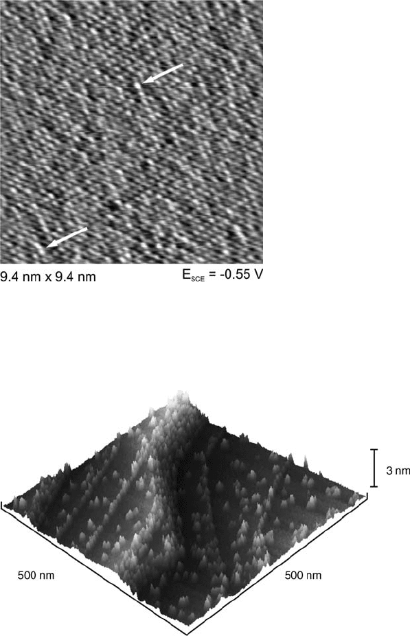
Figure 5.13 STM image of Pt clusters electrodeposited onto
Au(1 1 1) in 0.1 M H
2
SO
4
þ 0.1 mM K
2
PtCl
4
. E ¼þ0.1 V versus
SCE. (Reproduced with permission from Ref. [46].)
Figure 5.12 Atomically resolved STM image of a Pt
50
Ru
50
(1 1 1)
alloy electrode in 0.01 M NaF after annealing and cooling in H
2
/Ar.
The arrows mark bright spots that are assigned to Ru atoms.
(Reproduced with permission from Ref. [43].)
5.4 Strategies for Nanostructuring Surfaces
j
133