Cao Z. (Ed.) Thin Film Growth: Physics, materials science and applications
Подождите немного. Документ загружается.


6 Thin fi lm growth
© Woodhead Publishing Limited, 2011
AA
KK
IK
IK
BB
I
AA AA
=
KK – KK
–
,
BB BB
=
–
R,S
AA
R,S
AA
SR
KK
SR
KK
RS
IK
RS
IK
SR
IK
SR
IK
R,S
BB
R,S
BB
R
∫∫
∫∫
AA∫∫AA
BB∫∫BB
=∫∫ =
, ∫∫,
R,S
∫∫
R,S
AA
R,S
AA∫∫AA
R,S
AA
RS
∫∫
RS
SR
∫∫
SR
III
IK
IK
S
RS
IK
RS
IK
SR
IK
SR
IK
–
where K
X
= K
0
(X/l
s
), I
X
= I
0
(X/l
s
). The step velocity is obtained as the sum
of the adatom uxes from inner and outer terraces:
v
D
n
F
KK
II
IK
=
(
)
(
KK – KK
)
II) II
+ (
II+ (II
–
)
IK)IK
s
0s
v0
Rs
KK
Rs
KK
1
)
1
)
II) II
1
II) II
RR
II
RR
II
)
RR
)
II) II
RR
II) II
+ (
RR
+ (
II+ (II
RR
II+ (II
s
IK
s
IK
l
l
0s
l
0s
tr
F
tr
F
v0
tr
v0
–
v0
–
tr
–
v0
–
111
R
RS
SR
1
R
R
–
+
IK
RS
IK
RS
IK
SR
IK
SR
I
I
È
Î
Í
È
Í
È
Î
Í
Î
˘
˚
˙
˘
˙
˘
˚
˙
˚
[1.4]
where K
1
X
= K
1
(X/l
s
), and I
1
X
= I
1
(X/l
s
) are the modi ed Bessel functions
of order 1 (Finnie and Homma, 2000b).
1.3 Observation method of atomic steps
For the observation of atomic steps on growing surfaces, we employed in-situ
SEM. Atomic steps can be observed with a conventional SEM instrument,
but the contrast is so faint that it is easily hidden by the contamination of the
surface due to electron irradiation during SEM imaging. We used an ultrahigh
vacuum SEM instrument equipped with Knudsen cells for molecular beam
epitaxy (Homma et al., 1994). The secondary electron detector was set to
the side of the specimen in parallel to the axis of the specimen stage tilting.
The primary electron beam of 25 keV was incident at a grazing incidence,
5–30° to the surface, to enhance the sensitivity to the atomic scale surface
structures. In this article, the primary electron beam was incident from the
bottom direction of each image. The image foreshortening due to oblique
incidence is corrected in most images. The atomic steps appear bright when
the primary electron beam goes down the atomic step staircase, while they
appear dark when the primary electron beam goes up the staircase (Homma et
al., 1991). Another factor in uencing the atomic step contrast is the location
of the secondary electron detector (Homma et al., 1993b). When the primary
electron beam goes parallel to the atomic steps, the atomic steps appear
bright when the steps are facing the detector. Conversely, they appear dark
when they face away from the detector. Those are topographic contrasts of
atomic steps, which are similar to macroscopic scale step contrasts, and can
be used for imaging of steps as small as the monatomic layer of the crystal.
This observation method is used in Section 1.4.
an entirely different type of contrast can be used for atomic step imaging.
This is the surface phase contrast utilizing surface phase transition. In the
following, we explain the 7 ¥ 7–1 ¥ 1 contrast on Si(111) surfaces.
a clean Si(111) surface in ultrahigh vacuum takes a long range ordered
structure, the 7 ¥ 7 reconstruction, at below the transition temperature
(~860°C) (Florio and Robertson, 1970). The 7 ¥ 7 reconstruction starts to
occur at the atomic step edge during cooling from a high temperature. In
SEM images, a 7 ¥ 7 domain appears brighter than a 1 ¥ 1 domain without
ThinFilm-Zexian-01.indd 6 7/1/11 9:39:13 AM
7Measuring nucleation and growth processes in thin films
© Woodhead Publishing Limited, 2011
reconstruction (Homma et al., 1993a). Therefore, if 7 ¥ 7 domains form
continuously along an atomic step, the step is easily observed by SEM even
with a low magnication. One such method is to keep the sample 1–2°C
below the transition temperature, and observe thin 7 ¥ 7 domains along
atomic steps. another method is to rapidly quench the sample from above the
transition temperature towards room temperature, thus forming continuous
7 ¥ 7 domains along atomic steps.
The image in Fig. 1.2 was observed using the former method. Using a
Si(111) wafer with a small miscut angle, 0.01°, the sample was kept 1°C
below the transition temperature. The 1 ¥ 1–7 ¥ 7 phase transition starts
from the upper edge of an atomic step, and only a thin region of the upper
terrace becomes 7 ¥ 7 and appears bright. Since the width of continuous
7 ¥ 7 regions is negligible to the large step spacing, 1.5 mm, the atomic steps
are highlighted in the image. This method can be used for the observation of
atomic step behaviour not only at around the phase transition temperature but
also at higher temperatures by reducing the temperature just for observation
purposes.
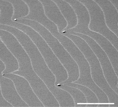
an example of the quenching method is shown in Fig. 1.3 (Homma and
Finnie, 2002). The Si sample with a at terrace as large as a 100 mm square
was rapidly quenched from 1230°C (see Section 1.5). Concentric atomic
steps with a spacing of ~20 mm can be seen. In between the concentric
steps there exist smaller circular steps. Those are monolayer holes on the
annular terraces. A magnied image of the small circular step is shown
in Fig. 1.3(b). The lower half of the atomic step appears bright, while the
5 µm
1.2 SEM image of atomic steps on Si(111) surface observed at the
1 ¥ 1–7 ¥ 7 phase transition temperature. Atomic steps are decorated
with continuous 7 ¥ 7 regions which appear bright in the SEM image.
ThinFilm-Zexian-01.indd 7 7/1/11 9:39:13 AM
8 Thin film growth
© Woodhead Publishing Limited, 2011
upper half appears dark. This contrast change is due to the difference in the
primary electron incidence relative to the atomic step edge, as explained
above. The topographic effect alone produces the atomic step image in SEM,
but the contrast is not high enough to be recognized in a low magnication
image.
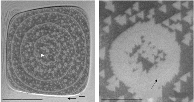
Both the upper and lower terraces near an atomic step turn to the 7 ¥ 7
phase after quenching. The width of the 7 ¥ 7 phase on the upper terrace
(outside of the hole) is 0.3–0.4 mm, and that on the lower terrace (inside of
the hole) is roughly twice as large. Therefore, the atomic step is observed
as a ~1 mm wide line. meanwhile, many triangular 7 ¥ 7 domains can be
seen on the terrace in the image shown in Fig. 1.3(b). Since these triangular
domains distribute discretely, only atomic steps continuously decorated by
7 ¥ 7 domains are highlighted in the low magnication image shown in
Fig. 1.3(a).
In Sections 1.5 and 1.6, we discuss the atomic step behaviour on Si(111)
surfaces at high temperatures based on observations using the quenching
method. although it is not a real-time observation method, the effect of
quenching on the step motion is negligible because phenomena occurring on
a large scale are observed on a huge terrace. It is interesting that macroscopic
observations by SEM in the 10–100 mm range can reveal phenomena
which relate to the attachment and detachment of atoms to/from atomic
steps.
50 µm
[1
12]
2 µm
Atomic step
(a) (b)
1.3 SEM image of atomic steps on Si(111) surface observed by the
quenching method (Homma and Finnie, 2002). Bright regions are
7 ¥ 7 reconstructed domains. (a) Low magnification image. (b) High
magnification image observed at the arrow head shown in (a).
ThinFilm-Zexian-01.indd 8 7/1/11 9:39:13 AM
9Measuring nucleation and growth processes in thin films
© Woodhead Publishing Limited, 2011
1.4 Two-dimensional-island nucleation and step-
flow growth modes
In MBE growth, two basic growth modes exist depending on the ratio of
the adatom diffusion length and the terrace width: the step-ow growth
mode where growth proceeds through atomic step progression, and two-
dimensional (2D) island nucleation growth mode where growth proceeds
through island coverage increase. Here, we show those two growth modes
on GaAs surfaces observed by SEM.
on a Gaas(001) surface, a monolayer step consists of Ga and as double
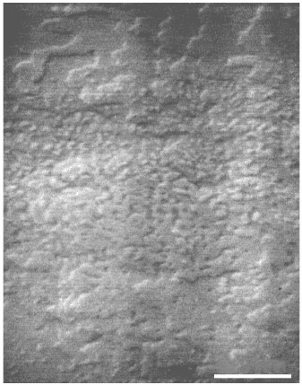
layers with a height of 0.28 nm. In Fig. 1.4, the process of one monolayer
evolution of a Gaas(001) surface is shown using the characteristic of
scanning imaging (Homma et al., 1995): acquisition of one image takes a
certain period while growth proceeds during the period. In the present case,
the image acquisition time and the monolayer growth period are 70 s and
50–55 s, respectively. Therefore, ~1.3 monolayers grow during one frame
imaging, and the process can be recorded in the image. Note that the growth
stage differs from the top to the bottom of the image. Growth started at the
beginning of imaging (at the top of the image). Initially, atomic steps are
visible. Then, small spots appear at about a quarter from the top. These
are 2D islands nucleating on the surface. Then, the islands grow rapidly
200 nm
1.4 SEM image of GaAs (001) surface during MBE growth (Homma et
al., 1995). Growth started at the top of the image and one monolayer
growth is completed at about three-quarters of the image length
from the top.
ThinFilm-Zexian-01.indd 9 7/1/11 9:39:13 AM
10 Thin film growth
© Woodhead Publishing Limited, 2011
in a lateral direction, causing coalescence of the islands. at three-quarters
from the top, holes are seen as the result of island coalescence, and nally
one monolayer is completed. atomic steps can be recognized at around the
completion of one monolayer. The second layer islands appear in the bottom
part of the image. In this way, an SEM image can record the growth of one
monolayer in real time for the 2D island nucleation growth mode. In the
initial period of one monolayer growth, islands are not observed. This is not
due to the resolution of SEM, but reects the surface reconstruction process
of Gaas(001) surface. In the 2 ¥ 4 structure, which is observed before MBE
growth, as atoms corresponding to quarter monolayer growth are lacking,
thus Ga atom rearrangement is necessary before island nucleation can occur
(osaka et al., 1995).
The reason for the use of a slow growth rate is to make the islands large.
The island size also relates to the surface diffusion length of adatoms. Thus,
the Ga-stabilized Gaas(111) surface (so-called (111)a surface), where the
surface diffusion length is much larger than that on the (001) surface, was
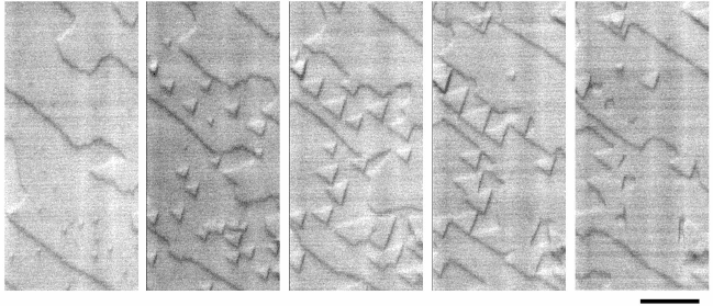
employed. The island growth process on this surface is shown in Fig. 1.5
(Yamaguchi and Homma, 1998). In this case, a higher image acquisition time
was used and the same area of the surface was repeatedly observed during
growth. owing to the large island size, nucleation, growth and coalescence
processes are clearly seen in Fig. 1.5. The islands are triangular, reecting
the three-fold symmetry of the (111) surface. Furthermore, step-ow growth
occurs without nucleation of island near the step edge. The step velocity is
higher parallel to the original steps than that in the perpendicular direction.
Precise analyses of the step velocity under different Ga supplying rate showed
500 nm
4 s 31 s 55 s 83 s 110 s
1.5 SEM image sequences showing the monolayer growth process
of GaAs(111)A surface (Yamaguchi and Homma, 1998). Each image
corresponding to 8 s growth starting from the time shown at the
top.
ThinFilm-Zexian-01.indd 10 7/1/11 9:39:13 AM

11Measuring nucleation and growth processes in thin films
© Woodhead Publishing Limited, 2011
that the step velocity was well described by Eq. 1.2 for an isolated step.
This is because the step spacing is much larger than the Ga diffusion length
on the Gaas(111)a surface. Fitting the measured step velocity dependence
on the Ga ux gave the Ga diffusion length of ~100 nm. Note that the step
spacing is more than 1 mm on the surface.
1.5 The motion of atomic steps on a growing and
evaporating Si(111) surface
Here, we consider the atomic step motion during evaporation at high
temperatures on the surface with an atomic step array with regular intervals
as shown in Fig. 1.6. a mathematical expression for this is given in the
appendix. on the high temperature surface, adatoms are released from
an atomic step and migrate freely onto the terrace. an atomic step acts
as an emitter and a sink of adatoms simultaneously, and thus the adatom
concentration at the atomic step reaches an equilibrium value. In the case of
evaporation, the adatom concentration at the middle of a terrace decreases due
to desorption. adatoms are supplied from the atomic step for compensation
of the decrease, causing retraction motion of the atomic step. This is the
step-ow evaporation. Adatoms can also be created directly on the middle
of a terrace, though the probability is small. In this case, an adatom and an
advacancy are created simultaneously. an advacancy can be annihilated by
recombination with an adatom. advacancies diffuse much more slowly than
adatoms, because an advacancy consists of surrounding surface atoms. When
the terrace size is large enough, the advacancy concentration at the centre
of the terrace increases to the extent that advacancies form 2D holes at the
centre of the terrace. This is the counterpart of the 2D island nucleation in
growth. Usually, only step-ow evaporation is observed on Si(111) surfaces,
because the diffusion length for adatoms is much larger than the atomic step
spacing on normal substrates.
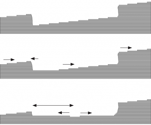
In the meantime, we consider a crater (hole) on a crystalline surface as
illustrated in Fig. 1.7. In the crater, there exists a slope whose inclination
Adatom
Advacancy
1.6 Schematic illustration of adatoms and advacancies on the high
temperature surface with atomic step allay.
ThinFilm-Zexian-01.indd 11 7/1/11 9:39:14 AM
12 Thin film growth
© Woodhead Publishing Limited, 2011
direction is opposite to the average inclination of the surface, i.e., the step-
ow direction is opposite to the average surface. Therefore, the very bottom
terrace of the crater expands during step-ow evaporation (Homma et al.,
1997). When the bottom terrace becomes large enough, a new terrace appears
due to 2D-macro-vacancy nucleation in the centre of the terrace. The lower
terrace expands in the same way as the initial terrace, and the macro-vacancy
nucleation is repeated. as a result, a set of concentric circular steps is created
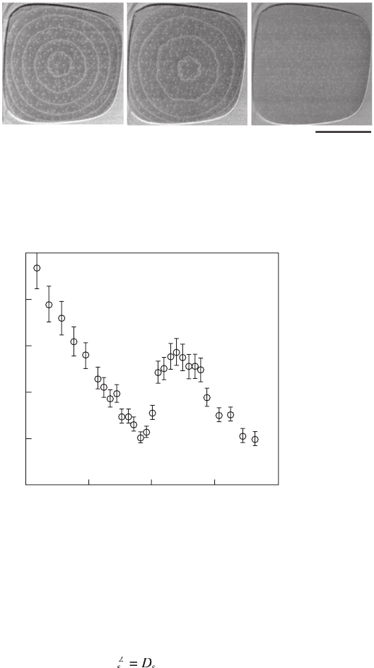
at the bottom of the crater as shown in Fig. 1.8. The spacing of the circular
steps is on the order of adatom diffusion length (see Section 1.9.2), and thus
varies with the temperature. Figure 1.9 shows the temperature dependence
of the atomic step spacing observed using a huge crater created on a Si(111)
surface by oxygen-ion bombardment in a secondary-ion mass spectrometer
(Homma et al., 1998).
The step spacing decreases with increasing temperature up to 1200°C. This
relates to the decrease in the surface diffusion length caused by the increase
in the desorption probability of adatoms: the surface diffusion coefcient D
s
is given by
D
s
= a
2
u
0
exp(–W
sd
/k
B
T)
where a is the lattice constant, u
0
is the frequency factor (~10
13
), W
sd
is the
energy barrier of surface diffusion, and T is the absolute temperature. The
Crater
~l
Step flow
(a)
(b)
(c)
1.7 Schematic illustration of step-flow evaporation of the surface
with a crater. (a) Initial surface. (b) Step-flow directions in the crater
during evaporation. (c) Macro-vacancy formation after the bottom
terrace size exceeds the adatom diffusion length.
ThinFilm-Zexian-01.indd 12 7/1/11 9:39:14 AM
13Measuring nucleation and growth processes in thin fi lms
© Woodhead Publishing Limited, 2011
desorption probability of adatoms is expressed using the desorption barrier
W
v
as
1/t
v
= u
0
exp(–W
v
/k
B
T)
Using Einstein’s formula
lt
s
lt
s
lt
2
lt
2
lt
sv
lt
sv
lt
lt
=
lt
lt
D
lt
, we get
l
s
= a exp[(W
v
– W
sd
)/2k
B
T]
The slope in the range of 1000–1200°C in Fig. 1.9 gives W
v
– W
sd
ª 2.4
eV.
The step spacing suddenly increases by a factor of 2.6 at around 1200°C,
50 µm
(a) (b)
(c)
1.8 SEM images of circular atomic steps on ultra-large terrace at the
bottom of a crater on Si(111) surface. The annealing temperature
before quenching is (a) 1180°C, (b) 1120°C and (c) 1020°C. No macro-
vacancy formation occurred in (c).
1000 1100 1200 1300 1400
Temperature (°C)
Step spacing (µm)
50
40
30
20
10
0
1.9 Temperature dependence of atomic step spacing observed on
ultra-large terraces formed at the bottom of a crater on Si(111)
surface (Homma et al., 1998).
ThinFilm-Zexian-01.indd 13 7/1/11 9:39:15 AM
14 Thin film growth
© Woodhead Publishing Limited, 2011
and decreases again for higher temperatures. This sudden increase suggests
occurrence of some transition on the surface. In fact, incomplete surface
melting, which is disordering of the rst layer in the double layers of the Si(111)
surface, has been observed by medium-energy ion scattering spectroscopy
at this temperature (Hibino et al., 1998). The surface structure transition
may affect the surface diffusion of adatoms. actually, the image shown in
Fig. 1.3 is the surface formed by quenching from 1230°C. Small circles are
seen between concentric atomic steps. These are monolayer holes located
at the middle of the annular terrace between the adjacent concentric steps.
When the sample passed through the transition temperature during cooling,
the adatom diffusion length suddenly decreased. This caused nucleation of
advacancy islands (monolayer holes) at the centre of the terrace as explained
above.
By varying the annealing temperature, the spacing of the concentric atomic
steps can be changed in the range 10–50 mm. If the annealing temperature
is set so that the step spacing is less than half of the bottom terrace size, no
nucleation of new islands occurs. Thus, an ultra-large terrace without atomic
steps inside can be obtained as shown in Fig. 1.8(c) (Finnie and Homma,
2000a).
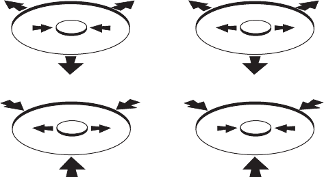
By using the ultra-large terrace created at the bottom of a crater, we can create
a monolayer island or hole by growth or evaporation. With the combination
of island or hole, and growth or evaporation, we can observe four cases as
shown in Fig. 1.10: island shrinkage and hole expansion during evaporation;
island expansion and hole shrinkage during growth. as an example, analysis
of evolution of circular terraces during growth and evaporation at 940°C is
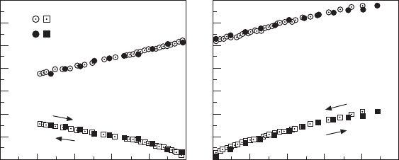
shown in Fig. 1.11 (Finnie and Homma, 2000b; Homma and Finnie, 2002).
The time evolution of the circular island and hole can be described by that
of their radii. Experimentally obtained step velocities were well tted to the
Island
Evaporation
Hole
Growth
1.10 Schematic illustration of step-flow growth and evaporation of
monolayer island and hole on a circular terrace.
ThinFilm-Zexian-01.indd 14 7/1/11 9:39:15 AM
15Measuring nucleation and growth processes in thin films
© Woodhead Publishing Limited, 2011
solution of the BCF equation on the cylindrical coordinate (Eq. 1.4). The
surface diffusion length of adatoms at 880°C estimated from the tting was
~50 mm, which is in good agreement with the step spacing in Fig. 1.9.
as seen in Fig. 1.11, the step progression and retraction are symmetric.
also, the behaviours of hole and island are symmetric. These indicate that
the contributions of upper and lower terraces are symmetric when adatoms
are incorporated into or released from atomic steps. In general, adatoms from
the upper terrace need to cross a higher energy barrier to be incorporated
into atomic steps than those from the lower terrace. This is called the
Ehrlich–Schwoebel barrier (Ehrlich and Hudda, 1966, Schwoebel and Shipsey,
1966). The present results indicate that the Ehrlich–Schwoebel barrier is not
signicant for the Si(111) surface at high temperatures.
1.6 Morphological instability of atomic steps
The Ehrlich–Schwoebel barrier is asymmetry in incorporating adatoms into a
step between those from the upper and lower terraces. Such asymmetry can
cause instability in step ow. Bales and Zangwill (1990) treated theoretically
the wandering of steps in step-ow growth and showed that when the ux
of adatoms from the lower terrace exceeds that from the upper terrace, the
uctuation in the atomic step is amplied, resulting in macro-scale step
wandering. This unstable growth regime is located between stable step ow
and 2D island nucleation in the phase diagram of growth mode as functions
of impinging ux and step spacing.
Radius (µm)
35
30
25
20
15
10
5
0
35
30
25
20
15
10
5
0
Evaporation
Growth
Outer hole
Outer hole
Island
Hole
G
G
E
E
–1000 –800 –600 –400 –200 0
Elapsed time (s)
0 200 400 600 800 1000
Elapsed time (s)
1.11 The radii of circular terraces as a function of annealing or
growth time observed at 940°C on the ultra large Si(111) terrace
(Homma and Finnie, 2002). The data for evaporation are overlaid
with those for growth by expanding the timescale of growth by
a factor of two. The time axis of growth is reversed to facilitate
comparison. Arrows indicate the direction of radius change during
evaporation (E) and growth (G).
ThinFilm-Zexian-01.indd 15 7/1/11 9:39:15 AM