Cao Z. (Ed.) Thin Film Growth: Physics, materials science and applications
Подождите немного. Документ загружается.


16 Thin film growth
© Woodhead Publishing Limited, 2011
As discussed above, the Ehrlich–Schwoebel barrier on the Si(111) surface
at high temperatures is small and this kind of step wandering is not observed.
Here, we show step instability in a different way. We utilized the fact that
the adatom ux to atomic step is an increasing function of the terrace width,
and distorted the symmetry between the upper and lower terraces by changing
the ratio of their sizes (Finnie and Homma, 2000c). This is possible only by
using an ultra-large terrace such as shown in Fig. 1.8(c).
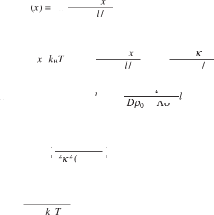
Figure 1.12 shows the time evolution of atomic step shape on a 100 mm
wide terrace (Homma et al., 2001). The observation was carried out using
a low Si molecular ux for nucleating only an island at the centre of the
terrace at 880°C. Each frame was observed by the quenching method after
growth duration starting from the at surface. This was to avoid any extra
nucleation due to repeated quenching. a small circular island is seen at the
centre of the terrace in image (a). This changes to the six-fold symmetry
island extending in <110> directions as seen in images (b) and (c). In this
stage, the peripheral atomic step progressing from the edge of the terrace is
smooth. after further growth, the periphery step becomes wandering as seen
in image (d). The wandering amplitude maximizes at 0.5 monolayers, and
then decreases for further growth as in image (e). The decay of wandering is
due to the stabilization of step ow when the upper terrace becomes large.
While the shape of the centre island reected the symmetry of the Si(111)
surface, the periphery step was initially smooth and became wandering
afterwards. This is exactly the result of step uctuation enhancement by the
large lower terrace.
[110]
[112
]
50 µm
(a)
(b)
(d)
(c)
(e)
1.12 SEM image sequences showing the evolution of atomic step
instability during growth at 880°C on the ultra large Si(111) terrace
(Homma et al., 2001). The images were obtained after growth of (a)
10 s, (b) 20 s, (c) 1 min, (d) 5 min and (e) 10 min.
ThinFilm-Zexian-01.indd 16 7/1/11 9:39:15 AM
17Measuring nucleation and growth processes in thin films
© Woodhead Publishing Limited, 2011
1.7 Conclusion and future trends
This chapter has shown that crystal growth of Si and Gaas in molecular beam
epitaxy is well described by the BCF model. That is, the surface diffusion
of adatoms is the dominant process of crystal growth and the incorporation
of adatoms into atomic steps is fast enough. on the evaporating surface, the
behaviour of advacancies is also well described by the BCF model. The key
to observe the atomic step motion of growing and evaporating Si surface at
high temperatures is the use of an ultra-large terrace created at the bottom
of a crater. Since the surface diffusion length of adatoms on a Si(111)
surface at high temperature becomes as large as 10–50 mm, a terrace width
comparable to the surface diffusion length is a prerequisite. SEM imaging
with the quenching method is useful for such a large-scale observation. In this
method, atomic steps were decorated with the 7 ¥ 7 phase domains. In order
to obtain an enhanced 7 ¥ 7 domain contrast, an oblique incidence of a 25 keV
primary electron beam was used. Recent progress in electron microscopy has
made it easier to observe atomic steps. A low energy SEM instrument with
a primary electron beam of 0.1–1 keV is commercially available these days.
Surface sensitivity is largely enhanced with the low energy beam, especially
when it is used in an ultrahigh vacuum. Low energy electron microscopy
(LEEM), which uses projection optics of reected electrons for imaging, has
realized real-time imaging of atomic steps even at elevated temperatures.
LEEM is now widely used for observation of growing surfaces of various
materials (Bauer, 1994; Meyer zu Heringdorf, 2008).
1.8 References
Bales G S and Zangwill A (1990) ‘Morphological instability of a terrace edge during
step-ow growth’, Phys. Rev. B 41, 5500–5508.
Bauer E (1994) ‘Low energy electron microscopy’, Rep. Prog. Phys. 57, 895–938.
Binnig G and Rohrer H (1983) ‘7 ¥ 7 reconstruction on Si(111) resolved in real space’,
Phys. Rev. Lett. 50, 120–123.
Burton W K, Cabrera N and Frank F C (1951) ‘The growth of crystals and the equilibrium
structure of their surface’, Phil. Trans. Roy. Soc. 243, 299–358.
Ehrlich G and Hudda F G (1966) ‘Atomic view of surface self-diffusion: tungsten on
tungsten’, J. Chem. Phys. 44, 1039–1049.
Finnie P and Homma Y (2000a) ‘Motion of atomic steps on ultraat Si(111): constructive
collisions’, J. Vac. Sci. Technol. A18, 1941–1945.
Finnie P and Homma Y (2000b) ‘Nucleation and step ow on ultraat silicon’, Phys.
Rev. B 62, 8313–8317.
Finnie P and Homma Y (2000c) ‘Stability–instability transitions in silicon crystal growth’,
Phys. Rev. Lett. 85, 3237–3240.
Florio J V and Robertson W D (1970) ‘Phase transformations of the Si(111) surface’,
Surf. Sci. 22, 459–464.
Hibino H, Sumitomo K, Fukuda T, Homma Y and Ogino T (1998) ‘Disordering of Si(111)
at high temperatures’, Phys. Rev. B 58, 12587–12589.
ThinFilm-Zexian-01.indd 17 7/1/11 9:39:15 AM
18 Thin film growth
© Woodhead Publishing Limited, 2011
Homma Y and Finnie P (2002) ‘Step dynamics on growing silicon surfaces observed
by ultrahigh vacuum scanning electron microscopy’, J. Cryst. Growth 237–239,
28–34.
Homma Y, Tomita M and Hayashi T (1991) ‘Secondary electron imaging of monolayer
steps on a clean Si(111) surface’, Surf. Sci. 258, 147–152.
Homma Y, Suzuki M and Tomita M (1993a) ‘Atomic conguration dependent secondary
electron emission from reconstructed silicon surfaces’, Appl. Phys. Lett. 62, 3276–
3278.
Homma Y, Tomita M and Hayashi T (1993b) ‘Atomic step imaging on silicon surfaces
by scanning electron microscopy’, Ultramicroscopy 52, 187–192.
Homma Y, Osaka J and Inoue N (1994) ‘In-situ observation of monolayer steps during
molecular beam epitaxy of gallium arsenide by scanning electron microscopy’, Jpn.
J. Appl. Phys. 33, L563–L566.
Homma Y, Osaka J and Inoue N (1995) ‘In situ observation of surface morphology
evolution corresponding to reection high energy electron diffraction’, Jpn. J. Appl.
Phys. 34, L1187–L1190.
Homma Y, Hibino H, Ogino T and Aizawa N (1997) ‘Sublimation of Si(111) surface in
ultrahigh vacuum’, Phys. Rev. B 55, R10237–R10240.
Homma Y, Hibino H, Ogino T and Aizawa N (1998) ‘Sublimation of a heavily boron-
doped Si(111) surface’, Phys. Rev. B 58, 13146–13150.
Homma Y, Finnie P and Uwaha M (2001) ‘Morphological instability of atomic steps
observed on Si(111) surfaces’, Surf. Sci. 492, 125–136.
Meyer zu Heringdorf F-J (2008) ‘The application of low energy electron microscopy and
photoemission electron microscopy to organic thin lms’, J. Phys.: Condens. Matter
20, 184007-1–184007-12.
Osaka J, Inoue N and Homma Y (1995) ‘Delayed and continuous nucleation of islands
in Gaas molecular beam epitaxy revealed by in situ scanning electron microscopy’,
Appl. Phys. Lett. 66, 2110–2112.
Osakabe N, Tanishiro Y, Yagi K and Honjo G (1980) ‘Reection electron microscopy
of clean and gold deposited (111) silicon surfaces’, Surf. Sci. 97, 393–408.
Pimpinelli A and Villain J (1994) ‘What does an evaporating surface look like?’, Physica
A 204, 521–524.
Schwoebel R L and Shipsey E J (1966) ‘Step motion on crystal surfaces’, J. Appl. Phys.
37, 3682–3686.
Swartzentruber B S (1996) ‘Direct measurement of surface diffusion using atom-tracking
scanning tunneling microscopy’, Phys. Rev. Lett. 76, 459–462.
Yamaguchi H and Homma Y (1998) ‘Imaging of layer by layer growth processes
during molecular beam epitaxy of Gaas on (111)a substrates by scanning electron
microscopy’, Appl. Phys. Lett. 73, 3079–3081.
1.9 Appendix
1.9.1 Extension of the Burton, Cabrera & Frank (BCF)
model for evaporating surface
This appendix discusses the behaviour of adatoms and advacancies on an
evaporating surface following the work by Pimpinelli and Villain (1994).
at high temperatures not far from the melting point, advacancies as well
ThinFilm-Zexian-01.indd 18 7/1/11 9:39:16 AM

19Measuring nucleation and growth processes in thin fi lms
© Woodhead Publishing Limited, 2011
as adatoms exist on the surface. We need to take advacancies into account
when we discuss the problems relating to evaporation on the surface. The
concentration of advacancy s(x) on the terrace has a minimum at the centre
of the terrace opposite to the concentration distribution of adatoms. When
the concentration of advacancy exceeds a certain value, a macro-vacancy,
one monolayer deep hole, is created.
To treat both advacancies and adatoms, we need to consider their pair
creation and pair annihilation. The annihilation rate of an adatom-advacancy
pair is proportional to the product of their concentrations, rs. The pair
creation rate at equilibrium is proportional to their equilibrium concentration,
r
0
s
0
. These values satisfy the coupled equations
r
.
= Dr≤ – r/t
v
+ D r
0
s
0
– D rs + F
s
.
= L s≤ + D r
0
s
0
– D rs
where D and L are the diffusion coef cients of adatoms and advacancies,
respectively, and ∆ is the proportional constant. To linearize the equations,
we introduce dr = r – r
0
and ds = s – s
0
, and suppose these are small (near
equilibrium). Also, we neglect the external ux F. Then, we get
dr
.
ª Ddr≤ – dr/t
u
– r
0
/t
u
– D r
0
ds – D drs
0
ds
.
ª Lds≤ – D r
0
ds – D drs
0
Since the step motion is much slower than the diffusion of adatoms and
advacancies, dr
.
= 0 and ds
.
= 0. Under the boundary conditions, r(± l/2) =
r
0
, s(± l/2) = s
0
, we get
dr
r
()
=
cosh
()
k
()
k
cosh
(2
k
(2
k
)
– 1
()x()
()x()
l
(2l(2
0
/
(2/(2
Ê
Ë
Á
Ê
Á
Ê
Ë
Á
Ë
ˆ
¯
˜
ˆ
˜
ˆ
¯
˜
¯
[a1.1]
ds
s
()
=
1 –
cosh
()
k
()
k
cosh
(/
k
(/
k
2)
0
()x()
()x()
l
(/l(/
Ê
Ë
Ê
Ë
Ê
Ê
Á
Ê
Ë
Á
Ë
Ê
Ë
Ê
Á
Ê
Ë
Ê
ˆ
¯
ˆ
¯
ˆ
ˆ
˜
ˆ
¯
˜
¯
ˆ
¯
ˆ
˜
ˆ
¯
ˆ
where
k
t
r
sr
2
0
00
sr
00
sr
=
1
+
sr
+
sr
sr
00
sr
+
sr
00
sr
v
D
sr
D
sr
sr
00
sr
D
sr
00
sr
L
In general, since adatoms diffuse much faster than advacancies, Dr
0
>> Ls
0
,
then, 1/k
2
ª Dt
v
= l
2
.
The step velocity for equidistant parallel steps is given by
v
D
n
dl
dx
n
dl
dx
=
2
2)
–
2
(2
dl(2dl
)
=
(
D( D
+
0
0
r
dl
r
dl
s
dl
s
dl
rs
(
rs
(
+
rs
+
0
rs
0
(
0
(
rs
(
0
(
(/
dl(/dl
/
(2/(2
L
L
rs
L
rs
000
0
)
t
an
h(
/2
)
n
l
kk
t
kk
t
an
kk
an
h(
kk
h(
ThinFilm-Zexian-01.indd 19 7/1/11 9:39:16 AM
20 Thin fi lm growth
© Woodhead Publishing Limited, 2011
1.9.2 Macro-vacancy formation
at high temperatures, the density of advacancies increases, resulting in the
formation of macro-scale vacancies of monolayer deep. The edge of the
macro-vacancy is an additional step. The formation of macro-vacancies is
described by nucleation theory. The free energy of a macro-vacancy with
radius R is expressed as
F(R) = 2pRg – pR
2
dm
where g is the step stiffness, and dm is the chemical potential. The rst term is
the energy increase due to step formation and the second term is the chemical
potential decrease due to formation of advacancy cluster. Since the density
of macro-vacancy is proportional to the Boltzmann factor, exp[–F(R)/k
B
T],
the clusters larger than the critical value R, which gives maximum of F(R),
expand, while those smaller than the critical value shrink. The maximum
of F(R) occurs at R
c
= g/dm,
F(R
c
) = pg
2
/dm
The condition for the formation of at least one macro-vacancy on the terrace
within the area of l ¥ l is
l
2
exp[–F(R
c
)/k
B
T] = l
2
exp[– pg
2
/dmk
B
T] ≥ 1 [A1.2]
Since r ~ r
0
,
r(x) = r
0
exp(–dm/k
B
T) [a1.3]
On the other hand, from Eq. A1.1,
rr
()
rr
()
rr
rr
=
rr
rr
rr
cosh
()
k
()
k
cosh
(2
k
(2
k
)
0
0
rr
()
rr
x
rr
()
rr
()x()
l
(2l(2
/
(2/(2
[A1.4]
By comparing these two equations, A1.3 and A1.4, we get
dm
()
dm
()
dm
/
= – ln
cosh
()
k
()
k
cosh
(2
k
(2
k
)
1 –
cosh
(
B
/
B
/
xk
()xk()
/ xk/
/ T/
()x()
k
()
k
x
k
()
k
l
(2l(2
k
(2
k
l
k
(2
k
/
(2/(2
@
kkk
x
kkk
x
kkk
l
)
cosh
(2
k
(2
k
l(2l
k
l
k
(2
k
l
k
)
/
(2/(2
at
at at
= 0,
(0
)/
8 =
/
(
+
)
B
22
0v
00
x
x
dm
(0
dm
(0
k
rt
/
rt
/
0v
rt
0v
/
0v
/
rt
/
0v
/
rs
(
rs
(
+
rs
+
00
rs
00
(
00
(
rs
(
00
(
+
00
+
rs
+
00
+
kT
B
kT
B
l
22
l
22
( D(
ª
/
L
rs
L
rs
00
rs
00
L
00
rs
00
lll
2
/8
Then, inserting this result into Eq. A1.2, we get
l
lk
2
2
22
lk
22
lk
B
2
exp
–8
()
lk()lk
T()T
B
()
B
≥ 1
pg
lk
k
lk
lk
22
lk
k
lk
22
lk
È
Î
Í
È
Í
È
Î
Í
Î
˘
˚
˙
˘
˙
˘
˚
˙
˚
or
8
pg
2
22
B
2
()
B
()
B
≤ 2 ln
lk
k
lk
k
22
lk
22
k
22
k
lk
k
22
k
()lk()
()T()
l
ThinFilm-Zexian-01.indd 20 7/1/11 9:39:17 AM
21Measuring nucleation and growth processes in thin films
© Woodhead Publishing Limited, 2011
Using typical step spacing l ~10
3
– 10
4
a,
g/k
B
T ≤ lk.
Since g is the order of k
B
T, we obtain the condition for macro-vacancy
nucleation,
l ≥ 1/k.
Using 1/k
2
ª Dt
v
= l
2
,
l ≥ l.
That is, a macro-vacancy is formed when the terrace size is comparable or
larger than the adatom diffusion length.
ThinFilm-Zexian-01.indd 21 7/1/11 9:39:17 AM

© Woodhead Publishing Limited, 2011
22
2
Quantum electronic stability of atomically
uniform films
T. Miller and T.-C. Chiang, University of illinois at
Urbana-Champaign, USa
Abstract: The valence electronic states in thin lms are quantized by the
lms’ boundaries. This represents a substantial modication of the band
structure of the system which inuences all physical properties. Dramatic
variations in thermal stability are observed in thin metallic lms on an
atomic layer-by-layer basis. This chapter describes measurements of
morphology, stability, and electronic structure of thin metallic lms using
angle-resolved photoemission spectroscopy, and discusses theoretical
models that can predict stability based on the quantization of states. Further
measurements using x-ray diffraction extend these results to structures more
complex than uniform lms.
Key words: quantum electronic stability, metallic quantum wells, thermal
stability, atomically uniform lms, angle-resolved photoemission.
2.1 Introduction
The valence electronic states in a solid-state system of nanoscale dimensions
are modied relative to their bulk counterparts by the presence of the system’s
boundaries. These modications, referred to generally as ‘quantum size
effects’ (QSEs), inuence all physical properties of the system. Of particular
interest here is the thermal stability of a thin lm. The rst section of this
chapter deals with the related idea of ‘electronic growth’ – the concept that
the growth mode of a lm can be governed to a large degree by the quantum
effects on the valence bands. Here we are considering metallic lms in which
the electronic states are most amenable to a relatively simple treatment and
competing effects are minimized. Next, angle-resolved photoemission (ARPES)
will be described as it is applied to thin lm studies. This is an important tool
for studies of these phenomena because, as applied to atomically uniform
lms, it can reveal the electronic structure of the system while at the same
time serving to precisely measure a lm’s thickness to an exact number of
monolayers. The growth and characterization of atomically uniform lms by
ARPES follows. Such lms may be of value for technological applications
because their unusual uniformity supports quantum states with a high degree of
coherence, and certainly they are important for scientic studies of quantum-
size effects because of their relative simplicity and ease of characterization.
ThinFilm-Zexian-02.indd 22 7/1/11 9:39:31 AM
23Quantum electronic stability of atomically uniform films
© Woodhead Publishing Limited, 2011
Next, measurements of quantum stability of some thin lm systems will be
presented. This will lead into a discussion of the general principles of thin
lm stability and their application to nanostructure development. Mostly this
is based on a simple picture of electronic quantization akin to the ‘particle-
in-a-box’ problem of elementary quantum mechanics. However, a section is
devoted to systems where the basic quantization conditions are modied by,
for example, specic substrate physical and electronic structures. Finally,
we speculate on what directions future research might be expected to take.
2.2 Electronic growth
Valence electrons are responsible for the bonding of the atoms or molecules
that make up a crystalline solid. In the case of a covalently bonded solid, it
is intuitive that the nature of the valence states would exert a dominant role
in the growth of a thin lm just as they do in the formation of a molecule,
via directional bonds and the lling of chemical orbitals, starting right from
bonding with the substrate. For a metallic overlayer, however, of all the
myriad factors inuencing lm growth, the valence electronic states of the
overlayer would perhaps seem to be at most a minor factor. Considering the
delocalized states of the metallic bond gives rise to a picture of lm growth
where kinetics, such as the lm/substrate lattice match and efciency of
packing, and bulk thermodynamic properties, such as surface tension and
melting point, are the driving forces shaping lm morphology. Electronic
effects due to the quantization of states by the boundaries of a smooth lm
have been discussed for some time, but their impact on lm properties, if
any, would be mitigated by a variety of effects, including loss of coherence
due to lattice mismatch and defects, and in any event would eventually
become irrelevant for lms thicker than a few monolayers (Feibelman
1983, Feibelman and Hamann 1984). Experiment has shown, however,
that this is not the case for well-ordered thin lms of nanoscale thickness,
where electronic effects can have a dramatic impact on thin lm properties
including surface reactivity (Danese, Curti et al. 2004, Zhang, Zhang et al.
2008), work function (Paggel, Wei et al. 2002), superconductivity (Guo,
Zhang et al. 2004), and surface energy and thermal stability (Czoschke,
hong et al. 2005). Coherent electronic behavior has also been observed in
lms thicker than 100 monolayers and even across a mismatched substrate/
lm boundary (Paggel, Miller et al. 1999b, Speer, Tang et al. 2006). It
is so that quantum-electronic inuences on metallic lm growth would
be expected to diminish with increasing thickness, but they are of direct
importance for practical applications as thicknesses of interest continue to
shrink, and indirectly for all deposited lms inasmuch as they start off as
nanolms where quantum effects should be considered in the establishment
of the initial growth modes.
ThinFilm-Zexian-02.indd 23 7/1/11 9:39:31 AM
24 Thin film growth
© Woodhead Publishing Limited, 2011
Of course, these quantum-mechanical effects are in competition with
kinetic constraints and, depending on one’s viewpoint, there are also different
aspects of electronic structure, such as charge spillage, Friedel oscillations
from either the substrate or the vacuum boundary, energy associated with
connement, etc., all of which may be in competition with each other in
determining the morphology of a growing lm (Zhang, Niu et al. 1998). Also,
the quantum effects being considered here arise from the overall geometry of
the system, and the growing lm may never have the opportunity to take a
suitable form for them to develop if kinetic constraints prevent it from doing
so from the initial stages of growth. The term ‘electronic growth’ has been
applied to deposition and annealing methods that permit quantum effects to
be expressed.
Early experimental work on electronic growth showed that atomically
at lms of Ag could be obtained on GaAs substrates by rst depositing
at low temperature and subsequently annealing to room temperature (RT)
(Smith, Chao et al. 1996). By starting at low temperature, kinetic effects
could be suppressed until enough material was deposited so that quantum
electronic effects could stabilize the formation of a at lm upon annealing
(Miyazaki and Hirayama 2008). More studies of low-temperature deposition
using reection high-energy electron diffraction with spot prole analysis
(RHEED-SPA) on Pb lms on Si(111) substrates revealed a preference
of island step heights of seven monolayers (Budde, Abram et al. 2000).
RHEED-SPA data contain information from a large area of the sample in
which there may be many small islands of different dimensions; later work
by the same group using scanning tunneling microscopy (STM) conrmed
these results and found also a preference for bilayer steps, and the authors
suggested a connection to quantum electronic effects (Hupalo, Kremmer
et al. 2001). Generally, these Pb lms consisted of islands with a distribution
of sizes sitting on top of a continuous wetting layer. With lower growth
temperatures, atomically uniform lms are possible in this material system
(Upton, Miller et al. 2004). For STM studies, a distribution of island sizes
may be a desirable feature, as the spectrum of preferred heights can be
directly measured on a single sample prepared at one time. However, in
islands, lateral connement occurs and the full three-dimensional structure
should be considered for theoretical treatment.
For fundamental studies of quantum electronic effects, a uniform thin
lm gives a simple interpretation in terms of one-dimensional quantum-well
states, leading to a more intuitive picture of the physics. Angle-resolved
photoemission is well suited for studies of uniform lms, and at the present
time a wealth of information is available from many photoemission studies
on quantum-well states in a variety of thin lm systems (Chiang 2000,
aballe, rogero et al. 2001, 2002, Bian, Miller et al. 2009, evans, alonso
et al. 1993, Liu, Paggel et al. 2008, Patthey and Schneider 1994). Even for
ThinFilm-Zexian-02.indd 24 7/1/11 9:39:31 AM
25Quantum electronic stability of atomically uniform films
© Woodhead Publishing Limited, 2011
these systems of relatively simple geometry, interactions between the lm
and substrate can give rise to quantized electronic structures of substantial
complexity (Liu, Speer et al. 2008).
2.3 Angle-resolved photoemission spectroscopy
ARPES is an experimental technique well suited for the measurement of the
electronic structure of solids. A monochromatic photon beam of sufcient
energy to overcome the sample’s work function is used to eject electrons
from the sample. The light source can be a laboratory one such as a resonance
lamp or a laser, or synchrotron radiation using a vacuum monochromator.
Synchrotron radiation is most versatile as the photon energy can be changed
over a continuous range. The electrons are collected by an analyser which
measures their angle of emission relative to the sample surface and their
kinetic energies. Since the photon is annihilated in the photoexcitation event,
energy conservation gives
E
kin
= hv – E
b
– W
where E
kin
is the measured kinetic energy, hv is the impinging photon
energy, E
b
is the binding energy of the electron inside the solid relative to
the Fermi level (E
F
) before excitation, and W is the work function. This
makes it possible to relate the measured energy spectra to the spectrum of
initial states inside the crystal (Hüfner 1995).
The energy states form a set of energy bands, each characterized by a
dispersion relation E
i
(k), where E is the energy, i is a band index, and k is
a wave vector referred to (somewhat loosely) as the ‘crystal momentum’.
Crystal momentum is analogous to momentum in free space, but takes into
account the fact that electrons in a crystal are diffracted by the xed lattice
and so are in states of mixed momentum. It is customary to label states
by the ‘reduced crystal momentum’ k which is the lowest value that could
be obtained by a hypothetical individual measurement of the electron’s
momentum, other values being possible from the same state by additions
from the discrete set of reciprocal lattice vectors. The set of all such k’s lls
the rst Brillouin zone of k-space (Ashcroft and Mermin 1976). An example
of crystal electronic structure is shown in Fig. 2.1, which shows calculated
bands of Ag along various directions within the rst Brillouin zone (Moruzzi,
Janak et al. 1978, Papaconstantopoulos 1986, Smith and Mattheiss 1974).
Knowledge of the emission angle and energy equates to knowing the
electron momentum after it has been emitted from the sample. Passing
through the surface, the translational symmetry of the lattice is preserved
in the surface plane, but not perpendicular to it, and likewise with the
crystal momentum. So, photoemission can characterize electronic states in
a crystal almost completely – the energy and the two in-plane components
ThinFilm-Zexian-02.indd 25 7/1/11 9:39:32 AM