Cao Z. (Ed.) Thin Film Growth: Physics, materials science and applications
Подождите немного. Документ загружается.

36 Thin film growth
© Woodhead Publishing Limited, 2011
This limits the number of peaks that can be seen in any given spectrum.
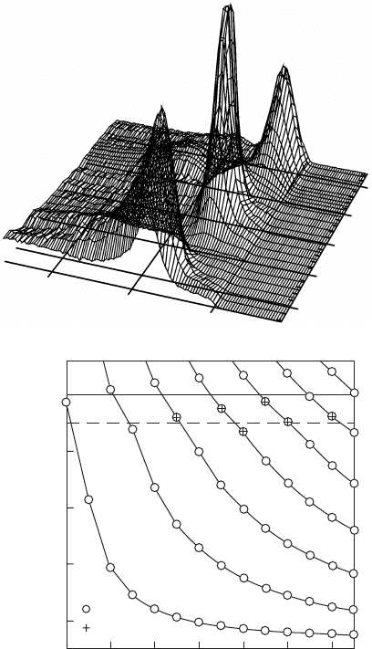
Figure 2.8 shows normal emission photoemission intensity as a function of
binding energy and lm thickness for a series of depositions ranging from
1.0
0.5
0.0
Binding energy (eV)
9
8
7
6
5
Thickness N (ML)
Binding energy (eV)
0
1
2
3
4
Fit
Expt
6
5
4
3
2
1
n = 0
0 2 4 6 8 10 12
Thickness (ML)
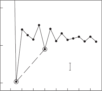
2.8 Top: 3-D mesh plot of normal emission photoemission intensity
as a function of binding energy and film thickness for Pb films on
Si(111). Bottom: modeled (circles) and measured (crosses) quantum-
well peak binding energies for Pb on Si(111). The model is fitted to
the measured peak positions and includes the band structure of Pb
and the phase shift. Quantum-well peak positions corresponding to
particular quantum numbers n are joined by lines. The dashed line
represents the position of the Si band edge: quantum confinement
in the film occurs for energies between the band edge and the Fermi
level at zero energy.
ThinFilm-Zexian-02.indd 36 7/1/11 9:39:35 AM

37Quantum electronic stability of atomically uniform fi lms
© Woodhead Publishing Limited, 2011
about 5 ML to 9 ML (Upton, Wei et al. 2004). Pairs of peaks like those in
Fig. 2.3 are not seen. However, for 6 ML no peak at all appears. The pattern
can be understood by reference to the plot of the binding energies of the
allowed states as a function of thickness shown in the bottom part of the
gure (Luh, Miller et al. 2002, Smith 1985, Upton, Wei et al. 2004, Wei
and Chou 2002). Over the thickness range from 5 to 9 ML there will be an
allowed quantum-well state between the Fermi level and the Si band edge
only for the odd thicknesses of 5, 7, and 9 ML. Starting at 5 ML and going
up in thickness a monolayer at a time, we see the state in the ‘con nement
gap’ for 5 ML being pulled down below the Si band edge at 6 ML, while
another allowed state is still above the Fermi level and so is unoccupied,
leaving no states to be seen with photoemission. Continuing up in thickness,
at 7 ML this unoccupied state becomes occupied and falls within the gap
region, and appears in the ARPES data. At 8 ML this state is just below the
gap. It actually does appear in the photoemission data as a weak, broad feature
– it is a quantum-well resonance that is not quite bound in the well. This
pattern prevents the observation of pairs of peaks characteristic of adjacent
monolayer thicknesses. On the other hand, the complete disappearance of
peaks when no states are within the con nement gap indicates that those
lms are in fact atomically uniform.
The alternating-layer pattern is re ected in the growth of Pb on Si and
diverse physical properties of lms, including their thermal stability and
even superconducting transition temperatures (Guo, Zhang et al. 2004). As
previously mentioned, preference for bilayer height steps in the population
of islands grown at different temperatures has been observed in STM
measurements (Hupalo, Kremmer et al. 2001, Hupalo and Tringides 2002).
The thermal stability of uniform Pb lms has been measured by photoemission;
results are shown in Fig. 2.9(a), where oscillations with a bilayer period are
seen (Upton, Wei et al. 2004). The physical basis for the bilayer pattern is
in the valence band structure. Along the (111) growth direction, the Pb sp
band crosses the Fermi level about halfway through the Brillouin zone. As
discussed above, sharp variations in physical properties are expected to be
related to quantum-well states crossing the Fermi level as the lm grows.
As a simple illustration, consider a case where the relevant band crosses
the Fermi level exactly in the middle of the zone. Ignoring the phase shift,
the allowed quantum-well states are determined by dividing up the zone by
the number of layers. It can easily be seen that as each layer is deposited,
the spectrum of allowed energies alternates between having a state right
at the Fermi level, or not. In fact, based on this picture, one can de ne a
periodicity for quantum property variations derived from the Fermi wave
vector k
F
along the growth direction:
D
h
k
=
F
k
F
k
p
ThinFilm-Zexian-02.indd 37 7/1/11 9:39:35 AM
38 Thin film growth
© Woodhead Publishing Limited, 2011
where Dh is the periodicity in thickness at which Fermi level crossings
occur and is equal to half of the Fermi wavelength. Here, h is dened as a
continuous variable, but a uniform lm is constrained to quantized values
that differ by integer numbers of monolayers. This discrete sampling is
important because it can lead to aliasing which produces very different
observed periods of oscillation in properties (Miller, Chou et al. 2009). A
related complication is the denition of the Fermi wave vector. For example,
using a free-electron value of k
F
= 1.58 Å
–1
for Pb lms gives Dh = 0.7 ML,
which is obviously not observed. However, taking into account the nite
sampling by monolayer increments, the aliased period is 2.2 Ml, a reasonable
value in line with observation. Accounting for the sampling in this case is
(a)
(b)
(c)
Expt
Pb films supported on Si
Theory
Envelope function
Theory
Envelope function
Freestanding Pb films
2 4 6 8 10 12 14
Thickness (ML)
250
200
150
0.1
0.0
–0.1
0.1
0.0
–0.1
Temperature (K)S (eV)S (eV)
2.9 (a) Measured stability temperatures for Pb films on Si(111) as a
function of thickness. Multiple measurements were made for most
thicknesses: the lines are guides to the eye connecting average
temperatures measured at each thickness. (b) Density-functional
calculation of the surface energy per site S for Pb films supported on
a Si substrate. Lines connect values calculated at integer monolayer
thicknesses. The dotted curves show an envelope function based
on a Friedel model; this illustrates the beating effect of sampling at
discrete thicknesses (Upton, Wei et al. 2004). (c) Similar to (b) except
for unsupported Pb films.
ThinFilm-Zexian-02.indd 38 7/1/11 9:39:35 AM
39Quantum electronic stability of atomically uniform films
© Woodhead Publishing Limited, 2011
equivalent to measuring the Fermi wave vector from the Brillouin zone
boundary instead of from the zone center (Wei and Chou 2002).
While 2.2 ML is not exactly an integer number of layers either, it is close
enough so that over a limited range of thicknesses, bilayer oscillations in
properties appear. However, over a great enough range the remainder becomes
signicant, leading to a beating effect and a phase reversal. Figure 2.9(b) is a
plot of the second derivative of the calculated surface energies per site from
rst-principles slab calculations of the electronic structure (Wei and Chou
2002). Analogous with the analysis of the previous section, this quantity
is a measure of the stability of a given thickness against bifurcation. The
calculated results reect the bilayer oscillations in the measured stability
temperatures. The theoretical values extend to greater thicknesses than the
experiment, and the beating effect leads to a diminishing of the quantum
oscillations and an even–odd phase reversal around 12 ML.
Previously, the importance of the phase shift was mentioned. The rst-
principles calculation presented in Fig. 2.9(b) includes implicitly the nature
of the interface between the lm and the substrate as well as the barrier
at the surface of the lm. This is built-in by having substrate layers and
vacuum layers as well as the lm material as part of the slab model used.
We note here that inclusion of the substrate is problematic – the interface is
mismatched and may involve reconstructions or special adlayers which are
only approximately handled in the calculation – and this could be the source
of some of the discrepancies in detail with the experimental result. In any
case, here the effects of the phase shift are implicitly included, and in fact
an effective phase shift can be extracted from the calculation if desired. One
can explore the effect of substrate interactions, for example, by removing
the substrate layers from the slab model. Results for such a calculation are
shown in Fig 2.9(c), which represents the stability function for a freestanding
Pb lm (Wei and Chou 2002). The important point to note here is that the
calculated result is very sensitive to changing the substrate interface. We
see cases of reversal in stability on a monolayer-by-monolayer basis, as
well as a large shift in the beating pattern. Again, one can look at this as
an indication of the sensitivity of quantum physical properties on the phase
shift.
The foregoing examples establish atomically uniform lms as an instructive
‘laboratory’ for the study of quantum-electronic stability. Spectra measured
with ARPES from such samples give both morphological and electronic
information at the same time. With the Pb on Si(111), a variety of growth
modes are possible, depending on the deposition temperature and annealing
recipes. How far can one go in applying the concepts learned from simple at
lms to more complicated morphologies? For the determination of morphology,
X-ray diffraction can be used and in some ways is more convenient than
photoemission. Thickness is determined by the appearance of multilayer
ThinFilm-Zexian-02.indd 39 7/1/11 9:39:35 AM
40 Thin film growth
© Woodhead Publishing Limited, 2011
interference peaks between the main Bragg peaks in the diffraction pattern.
Like photoemission, the measurement typically is macroscopic, the probe
beam typically being of millimeter to sub-millimeter size, so measurements
taken from a non-uniform sample will necessarily give superpositions of
patterns from different areas of the sample (Hong, Wu et al. 2000). However,
photoemission peak intensities can be difcult to interpret. For example, in a
spectrum from a sample composed of equal areas of 5 and 6 ML thicknesses,
the peak intensities associated with the two areas will in general not be
equal. Even worse, the relative intensities can vary markedly with changing
the exciting photon energy or the quantum numbers n of the states involved
(Paggel, Miller et al. 1999a). This is because photoexcitation involves a
matrix element that is sensitive to the relative phase of the initial and nal
state wavefunctions. In contrast, the analysis of X-ray diffraction data is a
rened art that is readily applied to thin lms.
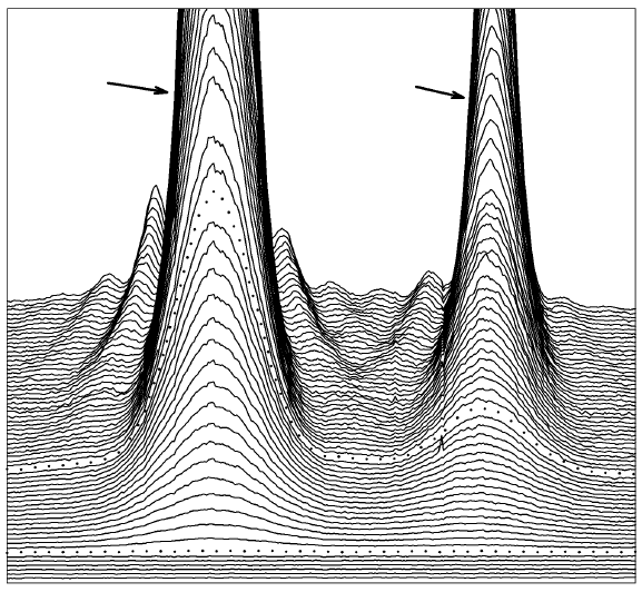
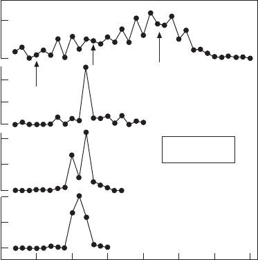
Figure 2.10 shows X-ray diffraction data from Pb deposited on Si(111)
at 180K (Hong, Wei et al. 2003). The stacked curves show the intensity
along the Pb(10L) truncation rod at different times during a continuous
deposition at a constant rate. The two main peaks are bulk Bragg peaks
as noted. Between these appear smaller satellite peaks from multilayer
diffraction – these peaks carry information about the thicknesses present on
the sample. The behavior of the diffraction can be summarized as follows:
rst, there is a period of time where Pb diffraction peaks do not appear. At
the same time, Si diffraction peaks (not shown) increase in intensity. This
is consistent with growth limited to an adlayer, commensurate with the
Si(111) surface. Then there is a period corresponding to about 1.5 ML of
total deposition where nothing really happens to the intensities, suggesting
Pb is present as a disordered gas on top of the adlayer. Beyond this point
Pb features abruptly appear. These features include both the bulk diffraction
peaks and satellite peaks, all of which increase in intensity as deposition
proceeds. The line shapes, however, remain the same during this time. The
pattern is characteristic of 5 ML high structures above the wetting layer,
or 6 ML altogether. Deposition beyond 6 ML causes the pattern to change
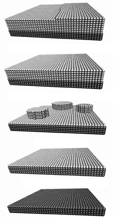
apparently in accord with layer-by-layer growth. The growth is summarized
schematically in Fig. 2.11 (Chiang 1997). First, Pb wets the surface. Subsequent
deposition leads to island growth, where all the islands are 6 ML high (from
the starting surface). Eventually a completely lled 6 ML lm is obtained,
followed by layer-by-layer growth.
This behavior can be understood by looking at a plot of surface energies vs.
lm thickness (Fig. 2.12) (Boettger, Smith et al. 1998, Chiang 2000, hong,
Wei et al. 2003, Kresse and Furthmüller 1996, Materzanini, Saalfrank et al.
2001, Wei and Chou 2002). This plot differs from the earlier one showing
the second derivative of the total energies because here we are not dealing
with bifurcation of a at layer, but rather a more general behavior, so there is
ThinFilm-Zexian-02.indd 40 7/1/11 9:39:36 AM
41Quantum electronic stability of atomically uniform films
© Woodhead Publishing Limited, 2011
need to examine the global energy landscape. The surface energy per surface
atom shows layer-by-layer variations but the important features are the deep
minima at 1 and 6 ML thicknesses. The energy of any conguration of only
these two thicknesses, considered as non-interacting regions, would lie on
the straight line segment shown between 1 and 6 ML. It is clear since this
line lies below all of the points for intermediate thicknesses that the system
will prefer to phase-separate into the wetting layer plus 6 ML high islands
for all intermediate amounts deposited.
So the physics of the at lm in this case predicts the behavior of a
slightly more complicated system of a wetting layer plus preferred-height
island growth. This study does not give information about the lateral size
distribution, but apparently this is not essential to the understanding of the
basics of growth. The growth temperature is important. For example, in Fig.
Pb (101)
Pb (102)
Intensity (arb. units)
Perpendicular crystal momentum L (arb. units)
2.10 X-ray diffraction intensities along the Pb(10L) rod during
deposition of Pb on Si(111). Time and the deposition amount
increase uniformly for each successive scan going up in the
figure; scans are displaced vertically for clarity. Two large peaks
characteristic of a 6 ML thick film are marked, smaller peaks between
these are multilayer diffraction for larger thicknesses. The dotted
curves indicate scans at 1.7 ML (lower dotted curve) and 5.7 ML
(upper dotted curve) thicknesses.
ThinFilm-Zexian-02.indd 41 7/1/11 9:39:36 AM
42 Thin film growth
© Woodhead Publishing Limited, 2011
2.12 we see also a signicant minimum in the energy at 4 ML. A system
prepared at low temperature could stay at that thickness rather than phase
separate. As a general yardstick for thermal energies, k
B
T, where k
B
is
Boltzmann’s constant and T is the temperature, can be used, and for 180K
Layer-by-layer growth
Islands merge into uniform film
Pb adlayer + islands of uniform height
Pb adlayer
Bare Si(111) substrate
2.11 From bottom to top, schematic of the growth of Pb on Si(111).
After completion of an adlayer, growth favors the development of
multilayer islands of uniform height, followed by layer-by-layer
growth.
ThinFilm-Zexian-02.indd 42 7/1/11 9:39:36 AM
43Quantum electronic stability of atomically uniform films
© Woodhead Publishing Limited, 2011
is shown by a bar in Fig. 2.12. Evidently this is large enough compared to
the layer-by-layer variations between 1 and 6 ML so the system does not get
‘stuck’ at 4 ML at this temperature. It is reasonable that if the temperature
is chosen suitably the bilayer oscillations in favored thicknesses would be
seen instead of this phase separation.
Another X-ray diffraction study was reported on this system that explicitly
explored the role of the temperature on lm morphology. Figure 2.13
(Czoschke, Hong et al. 2005) shows the fraction of a surface covered by
Pb islands of different heights, starting with an 11 ML thick nearly uniform
lm and subsequently annealing to the temperatures indicated. 11 ML is
an unstable thickness, and with heating it starts to bifurcate and appears
to be fully bifurcated into regions of 10 and 12 ML at 200K. Annealing
further, we see the development of a single peak at 12 ML. From the surface
energy, 10 ML should be more stable than 12 ML; however, the system
started with 11 ML and the total amount of material must be conserved. To
accommodate this, the system can have 12 Ml islands separated by some
amount of the very stable wetting layer. At higher temperatures, the lm
becomes disordered, and at 280K it has reached a state of local thermodynamic
equilibrium with many thicknesses present. Inspection of the top curve shows
that the distribution of island heights is not random, but follows what is by
now a familiar pattern – a jagged series of bilayer oscillations but with the
appearance of occasional phase reversals (beating effect) indicated by the
Pb/Si films
k
B
T
0 2 4 6 8 10 12 14 16
Film thickness (ML)
Relative surface energy (eV)
–0.6
–0.7
–0.8
2.12 Relative surface energy derived from a density-functional
calculation for different thicknesses of Pb on Si(111). Dots are
calculated values and lines are guides to the eye. The dashed line
joining the points at 1 and 6 ML thicknesses represents the energy
of a system consisting of the adlayer plus 5 ML high islands with
average thickness as plotted. The ‘error bar’ shows the scale of
thermal energy at the growth temperature.
ThinFilm-Zexian-02.indd 43 7/1/11 9:39:36 AM
44 Thin film growth
© Woodhead Publishing Limited, 2011
arrows in Fig. 2.13. Indeed, with suitable thermodynamic analysis, data
such as these can be related to the calculated surface energies with good
agreement. It is perhaps remarkable that even in this ‘more realistic’ system,
which should involve many complicating factors such as lateral connement,
shape effects, registry with the substrate, etc., the simple picture afforded
by atomically uniform lms still gives essential insight as to its quantum
electronic stability.
The importance of the phase shift has been demonstrated and emphasized in
the foregoing. A natural question is, can one inuence growth by adjustment
of the phase shift by modication of the surface or substrate interface? The
encouragement of layer-by-layer growth modes through the use of surfactants
has been studied and reported on in the literature. As the name implies, these
are expected to operate by reducing the surface energy. Typically, a foreign
species is introduced at the start of growth that tends to ‘oat’ on the surface,
stabilizing it. In some sense this is a ‘catalytic’ process in that the surfactant
is not consumed but acts continuously as growth proceeds (Rioux and Höchst
1992). However, typically these are viewed as acting locally, for example
by saturating the surface dangling bonds, and do not involve states in the
bulk of the lm. For the purpose of exploiting quantum electronic effects to
inuence stability, intuitively it would seem to be much easier to modify the
Local equilibrium
253 K
Preferred height islands
110 K
Initial 11 ML deposit
200 K
Bifurcation
280 K
Pb on Si(111)
Annealing
0 5 10 15 20 25 30 35
Film thickness (ML)
% Surface area covered
5
0
40
20
0
40
20
0
20
0
2.13 Distribution of thicknesses of Pb on Si(111) as annealling
proceeded following an initial 11 ML deposition, derived from
X-ray diffraction measurements. The arrows mark points where
the alternating layer pattern of stability switches from even to odd
numbers of monolayers and vice versa.
ThinFilm-Zexian-02.indd 44 7/1/11 9:39:36 AM
45Quantum electronic stability of atomically uniform fi lms
© Woodhead Publishing Limited, 2011
phase shift at the substrate/ lm interface than at the surface. However, for
fundamental studies it is important that the interface remain well ordered. For
Pb on Si(111), one can make several well-ordered reconstructed surfaces using
‘foreign’ atoms and still be able to grow Pb lms on top. It turns out that by
doing so, it is indeed possible to tailor the landscape of thermal stability in
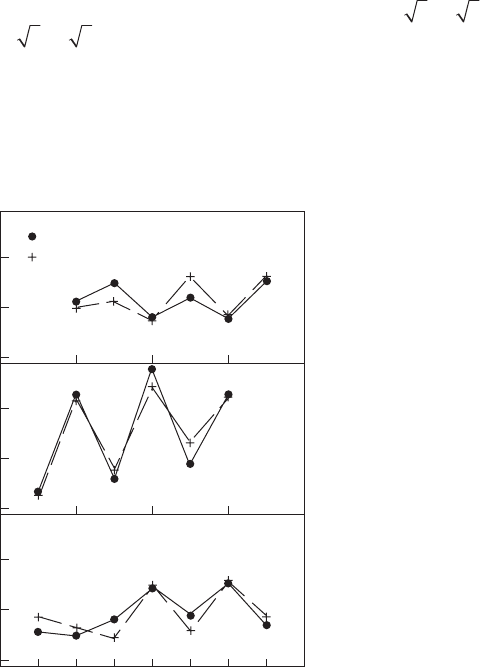
a dramatic fashion. Figure 2.14 shows results of experiments using Au and
In as ‘interfactants’, compared to a straight Pb system (Ricci, Miller et al.
2005). These systems were prepared by rst depositing the interfactant atoms
and annealing to produce the following ordered surfaces: In
(3
(3
3
¥
)
, Au
(6 ¥ 6), and Pb
(3
(3
3
¥
)
. The amounts of the interfactant materials to make
these reconstructions are 0.333, 0.96, and 0.33 ML, respectively. Here a ML
is de ned to be with respect to the Si(111) surface layer. Then, Pb layers
were grown on top at 60K. The thermal stability was measured in the same
way that has been outlined earlier, using photoemission to monitor the lm
structure. The interfactant atoms at the substrate surface change the interface
2.14 Stability temperatures for Pb fi lms on Si(111) as a function of
fi lm thickness using three different interfactants, (a) In, (b) Au, and
(c) Pb. The dots joined by solid lines are experimentally measured
points, the crosses joined by dashed lines are a fi t to a model from
which the phase shift can be extracted (Ricci, Miller et al. 2005,
Czoschke, Hong, et al. 2005). The same scales are used in all three
panels so that the effect of the interfactant on thermal stability is
directly visible.
Expt
Fit
Pb/In/Si(111)
Pb/Au/Si(111)
Pb/Pb/Si(111)
2 3 4 5 6 7 8 9 10
Thickness (ML)
Stability temperature (K)
300
200
100
300
200
100
300
200
100
(a)
(b)
(c)
ThinFilm-Zexian-02.indd 45 7/1/11 9:39:37 AM