Fahlman B.D. Materials Chemistry
Подождите немного. Документ загружается.

valence electron (i.e., possess a low work function). The holes that migrate from the
anode are blocked from further transport to the cathode by an organic layer of 2,9-
dimethyl-4,7-diphenyl-1,10-phenanthroline (BCP, Figure 4.79c), which has a rela-
tively low-lying HOMO.
In contrast, the anode is usually tin-doped In
2
O
3
(ITO, typically 1:9 Sn:In), since
this material is transparent and highly conductive (ca.1 10
4
W
1
cm
1
).
[84]
The substitutional replacement of In
3+
ions with Sn
4+
ions results in n-doping of
the lattice, injecting electrons into the conduction band. The doping of Sn into the
In
2
O
3
lattice may also result in SnO sites; this introduces holes in the lattice that
reduces its conductivity. The conductivity of ITO is due to both Sn dopants and O
vacancies, as represented by the general formula In
2x
Sn
x
O
32x
.
[85]
Since the
organic hole-transport polymer is in direct contact with ITO in an OLED, the surface
properties of ITO is important for effective hole injection. It has been shown that
surface treatments such as UV ozone cleaning or Ar/O
2
plasma treatments, result in
an increase in the work function of the ITO surface as the Sn :In ratio is decreased
(and O concentration is incr eased).
The recombination of a hole and electron creates a quasiparticle known as an
exciton, which releases a photon of energy. Organic molecules in the emissive layer
facilitate exciton formati on – likely through hole-trapping, followed by Coulombic
attraction to the free electrons. A challenge in OLED design is to ensure that an
equal number of holes and electrons meet in the emissive layer. This is not trivial,
since holes migrate much slower than electrons in conductive organic molecules.
The organic molecules used in OLED s/PLEDs are p-conjugated, meaning that p
z
orbitals on adjacent (–C¼C–C¼)
n
units overlap, resulting in p valence and p
*
conduction bands. The observed color will depend on the HOMO–LUMO gap of
the molecule, which may be fine-tuned by altering the length of the conjugation,
or nature of the molecular backbone (e.g., substitution of electron withdrawing/
donating groups, etc.).
A limitation of traditional OLEDs/PLEDs is their relatively poor quantum effi-
ciency. An exciton may exist in either a single t (total spin, S ¼ 0) or triple t state
(S ¼ 1), with the triplet outweighing the singlet by a 3:1 ratio. The molecules in the
emissive layer are referred to as fluorophores, which yield fluorescent radiation only
when a singlet exciton is formed. Hence, the theoretical maximum efficiency that is
possible is only 25%. In an effort to improve the efficiency, a number of recent
studies have been devoted to using organometallic compounds (transition metals
with organic ligands), which allow for rapid intersystem crossing (ISC) from the
excited singlet to light-emitting triplet states (Figure 4.80). The process of collecting
the excitons in the lowest excited triplet state is referred to as triplet harvesting,
and results in a 100% quantum efficiency of the OLED.
[86]
This effect is most
pronounced for complexes of 4d and 5d transition metals with well-shielded valence
electrons, which exhibit large spin–orbit coupling
[87]
and concomi tant mixing of
singlet and triplet states.
[88]
328 4 Semiconductors

Figure 4.80. Illustration of triplet harvesting. In the absence of a triplet emitter, the triplet excitation
energy is converted to heat, losing 75% of the quantum efficiency. Also shown are a variety of
organometallic complexes, and their relative spin–orbit coupling values – directly proportional to their
use in phosphorescent OLEDs. Reproduced with permission from Yersin, H. Top. Curr. Chem. 2004, 241,
1. Copyright 2004 Springer Science and Business Media.
4.3. Light-Emitting Diodes: There is Life Outside of Silicon! 329
4.4. THERMOELECTRIC (TE ) MATER IALS
As our society attempts to wean itself from a dependence on fossil fuels, many
alternative energy sources are being investigated. One interesting potential is from
the conversion of waste heat (e.g., vehicle engine heat) into electricity. This conver-
sion is due to the thermoelectric effect, first discovered for junctions (or thermocou-
ple) of two dissimilar metals. When metals are welded together, free electrons are
able to drift across the junction in a preferential direction, based on the different
atomic lattice structures of each metal. The migration of electrons effectively leaves
one metal electron-deficient (positively charged), and the other metal negatively
charged.
If the two metals are held at different temperatures, a voltage will result that is
proportional to the DT. The ratio (DV / DT) is referred to as the Seebeck coefficient,
a, related to the band structure of the materials involved. The a value for semicon-
ductors is at least two orders of magnitude larger for semiconductors relative to
metals, giving rise to much greater voltages. Contrary to the Seebeck effect, when a
current is passed through a closed circuit of the two metals, heat is produced at one
of the junctions and is absorbed at the other. Since the latter junction is cooled, this
Peltier effect has been largely exploited for thermoelectric cooling applications
(e.g., auto seat coolers, com puter component cooling).
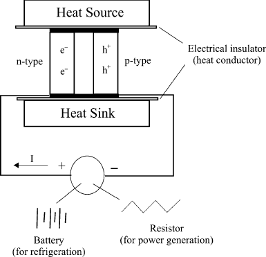
A TE device consist s of a heat source and sink, joined together via n-type and
p-type semiconductor materials (Figure 4.81).
[89]
The figure of merit, ZT (Eq. 22), of
the device is useful to determine its suitability for power generation or refrigeration –
a means to describe the transport properties of the TE material. An effective TE
Figure 4.81. Schematic of a thermoelectric device, which may be used for power generation or
refrigeration.
330 4 Semiconductors

material should have a high Seebeck coefficient (heat conversion efficiency) and
electrical conductivity, as well as low thermal conductivity to maintain thermal
isolation in the device. The thermal conductivit y is related to the transfer of heat
through a material through either electron transport or quantized lattice vibrations
(phonons). Hence, the ideal TE material has been described as a phonon-glass/
electron-crystal, having the electrical properties of a crystalline lattice, and thermal
properties of an amorphous/glass-like solid.
ZT =
a
2
s
l
ð22Þ
where a is the Seebeck coefficient (mVK
1
; 1–10 for metals, 150–250 for
semiconductors); s is the electrical conductivity; and l is the thermal conductivity
(electronic + lattice terms).
Semiconductors are much more effective TE materials (greater ZT values) than
metals due to their significantly greater Seebeck coefficients and lower thermal
conductivities. A barrier toward higher ZT values for semiconductors is their
relatively small electrical conductivity, especially at low temperatures. In order
to overcome this limitation, the chemical composition of the semiconductor may
be fine-tuned to yield a small bandgap material (6k
B
T; k
B
¼ Boltzmann cst;
i.e., 0.16 eV at 300 K), o r one that is sufficiently doped with an intermediate
concentration (ca.10
19
–10
21
cm
3
) of electroni c/thermal carriers exhibiting high
mobility through the lattice.
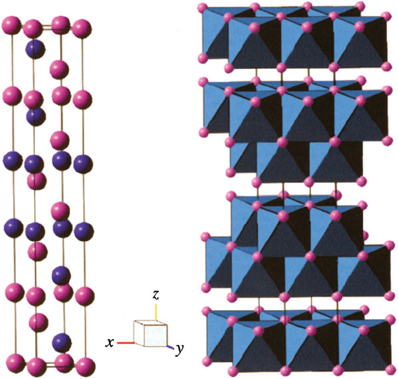
The most widely studied TE material is Bi
2
Te
3
, consisting of a hexagonal unit
cell with repeating...[Te–Bi–Te–Bi–Te...Te–Bi–Te–Bi–Te]...units (Figure 4.82).
Whereas Te–Bi layers are bound by strong covalent interactions, the bonding
between adjacent Te layers is through weak van der Waals interactions. This results
in bulk anisotropic electrical and thermal conductivity, being most pronounced
along planes that are perpendicular to the c-axis of the unit cell. To further improve
ZT values, Bi
2
Te
3
crystals may be doped with n- or p-type dopants, with most
desired compositions of Bi
2
Te
2.7
Se
0.3
(n-type) and Bi
0.5
Sb
1.5
Te
3
(p-type), yielding
ZT ¼ 1 at room temperature. This improvement results from a decrease in thermal
conductivity of the lattice, brough t about by phonon scattering by the dopant atoms
(i.e., perturbing the symmetry of the lattice, affecting the organized lattice vibration
modes).
The following list represents the primary materials classes that have been
designed in an effort to optimize ZT for thermoelectric applications.
[90]
The general
strategy is to dope the lattice with sufficient carriers (n- or p-dopants), while also
interrupting the phonon transport through the solid through the introduction of large
interstitial atoms.
(i) Complex Solid-State Inorganic Lattices (e.g., CsBi
4
Te
6
,Bi
2x
Sb
x
Te
3y
Se
y
,
ZrTe
5
,Ag
n
Pb
m
M
n
Te
m+2n
(M ¼ Sb, Bi), AgPb
10
SbTe
12
, “Half-Heusler alloys”
MNiSn (M ¼ Zr, Hf, Ti), Zr
0.5
Hf
0.5
Ni
0.5
Pd
0.5
Sn
0.99
Sb
0.01
). For half-Heusler
alloys, the unit cell is a combination of a NaCl lattice of two metals, with the
third metal occupying tetrahedral interstitial sites. For instance, for TiN iSn,
4.4. Thermoelectric (TE) Materials 331
the Ti and Sn form the NaCl lattice, with Ni occupying 1/2 of the available
tetrahedral interstitial sites (i.e., Ti:Ni:Sn ¼ 4:4:4 atoms per unit cell). This
combination offers a great deal of control over electronic/thermal conductivity
of the solid. While the introduction of Sn (p-doping) increases electrical conduc-
tivity, heavy metal atoms such as Ti and Ni cause a decrease in thermal
conductivity through phonon scattering.
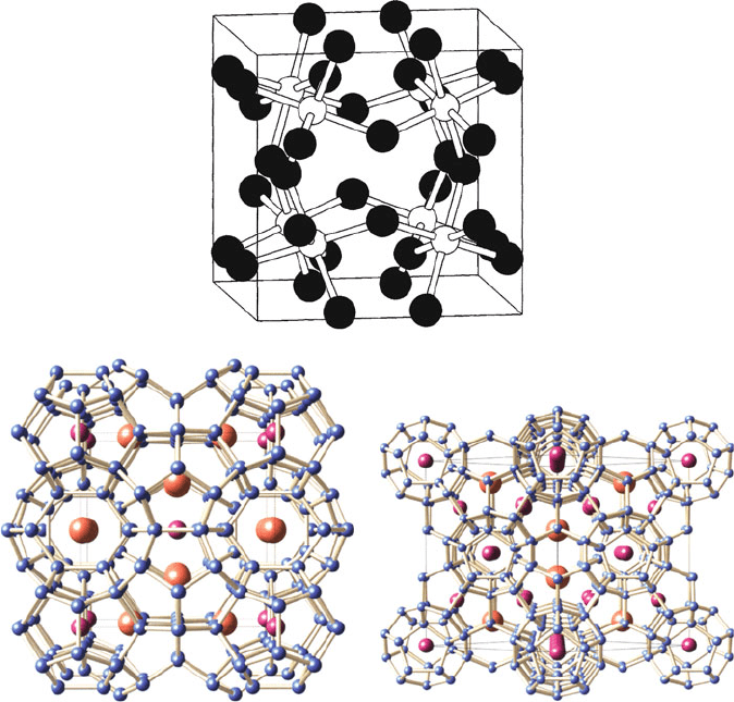
(ii) Crystal Structures with “Rattlers” (e.g., Rare-earth (e.g., La, Ce, Nd, Sm, Eu,
etc.) doped AB
3
-based (A ¼ Co, Fe, Ru, Os, Ir; B ¼ P, As, Sb), Figure 4.83),
[91]
or complex antimonide skutterudites (e.g., b-Zn
4
Sb
3
,Yb
14
MnSb
11
,
A
y
Mo
3
Sb
7x
Te
x
),
[92]
or clathrates (e.g.,Ba
8
Ga
16
E
30
,E¼ Ge, Si)(see endnote
89). In these structures, dopant atoms are weakly bound to the cage, and “rattle”
in resp onse to increasing temperature. As the atom within the cages becomes
smaller/heavier, the amount of structural disorder will increase causing a larger
decrease in lattice thermal conductivity.
(iii) Oxides (e.g., NaCo
2
O
4
,Ca
3
Co
4
O
9
,
[93]
Al
0.02
Zn
0.98
O, b-SrRh
2
O
4
[94]
). These
structures consist of CoO
x
layers, which serve as effective electronic transport
Figure 4.82. Unit cell of Bi
2
Te
3
– a widely studied thermoelectric material. The blue atoms are Bi, and
the pink atoms are Te. Reproduced with permission from Tritt, T. M.; Subramanian, M. A. MRS Bull.
2006, 31, 188. Copyright 2006 Materials Research Society.
332 4 Semiconductors
media within the latt ice. A variety of metal/metal oxide layers (e.g., Na, Ca, Sr,
Bi) are placed in between the metal oxide layers to serve as phonon scatterers
(Figure 4.84).
(iv) Nanoarchitectures (e.g., PbTeSeTe/ PbTe quantum dot superlattices, nanowires
(Bi
2
Te
3
[95]
, PbSe
[96]
, etc.), nanoporous silicon,
[97]
and “nanoparticle-in-alloy”
materials
[98]
). The electrical and thermal conductivities of a bulk material are
strongly coupled, which makes it difficult to increasingly improve ZT values.
However, in a solid with at least one dimension in the nanoregime, one may
Figure 4.83. Crystal structures of an unfilled IrSb
3
skutterudite (top – Sb atoms shown in black) and
Type I/Type II clathrates (bottom). In the skutterudite structure, a void is present in the center of the
unit cell, surrounded by 12 Sb atoms. For the clathrate structures, tetrahedrally bound framework atoms
(e.g., Ge, Sn, Si) are illustrated in blue, and guest atoms within the various cages are shown in orange
and pink. Reproduced with permission from (i) Nolas, G. S.; Poon, J.; Kanatzidis, M. MRS Bull. 2006, 31,
199. Copyright 2006 Materials Research Society and (ii) Chem. Mater. 2000, 12, 697. Copyright 2000
American Chemical Society.
4.4. Thermoelectric (TE) Materials 333
dramatically alter the carrier- transport properties by simply varying its dimen-
sions due the confinement of the carriers inside the material.
[99]
We will discuss
quantum confinement within nanostructures in more detail in Chapter 6 .
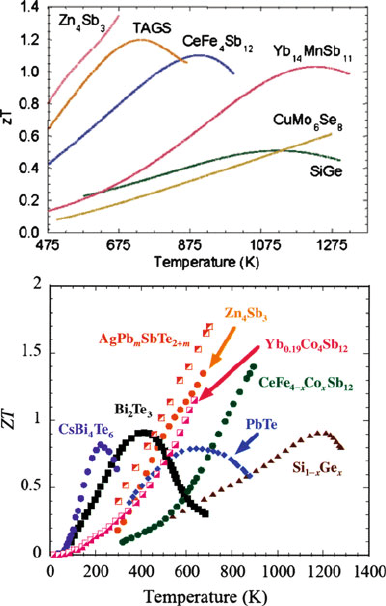
The comparison of ZT values for a host of the above bulk materials is displayed
in Figure 4.85, along with the variation of ZT with temperature. The search for
new TE materials continues to be an extremely active area of research; recent
work has resulted in suitable TE components at virtually all temperature regimes.
However, the search continue s for materials with ZT values in excess of 2.0. Though
most bulk materials exhibit figure-of-merits 1.5, certain types of nanomaterials
are the only candidates to date with ZT values >2.0 – yet another triumph of
nanotechnology!
[100]
IMPORTANT MATERIALS APPLICATIONS III: PHOTOVOLTAIC
(SOLAR) CELLS
The increasingly volatile prices and availability of gasoline and natural gas, and the
recent British Petroleum oil spill disaster has brought about a heightened awareness
of our dependence on nonrenewable resources. Currently, over 90% of the US
electricity supply comes from the combust ion of fossil fuels (i.e., coal, oil, and
natural gas) and nuclear power generation.
While the US coal reserve is estimated at 290 billion tons (enough to last another
230 years at current production levels), there is an increased concern about the
adverse environment al effects associated with its combustion, namely SO
x
,NO
x
,
and CO
2
emissions. With the energy needs of our world likely to double within our
Figure 4.84. Crystal structure schematic of CoO
2
-based TE oxides. Shown are (a) Na
x
CoO
2
, (b)
Ca
3
Co
4
O
9
, and (c) Bi
2
Sr
2
Co
2
O
y
. Reproduced with permission from Koumoto, K.; Terasaki, I.;
Funahashi, R. MRS Bull. 2006, 31, 206. Copyright 2006 Materials Research Society.
334 4 Semiconductors
generation, there continues to be active development of alternative renewable
energy sources. In an earlier chapter, we dealt with hydrogen-based fuel cells; we
now will describe another extr emely attractive option – harvest ing the unlimited
power from the sun.
The majority of commercial photovoltaic cells utilize silicon-based technology.
When sunlight comes in contact with a p–n diode, the absorbed energy causes
promotion of electrons from valence to conduction bands, generating additional
electron-hole pairs (EHPs). Since the n-side is much thinner than the p-side, most of
the photons are absorbed within the depletion region and p-side. The most noticeable
result of this excitation is an effective increase in the number of electrons in the
conduction band of p-Si (or holes in n-Si, referred to as the minority-carrier
concentration). As a result, electrons in the p region will diffuse into the depletion
region, where the junction potential (Figure 4.86a, E
o
) propels them back into n-Si
(vice versa for holes). It is important to note that only EHPs that are generated within
Figure 4.85. The temperature dependence of ZT values for various TE materials. TAGS refers to
(GeTe)
0.85
(AgSbTe
2
)
0.35
. Reproduced with permission from Tritt, T. M.; Subramanian, M. A. MRS
Bull. 2006, 31, 188, and Chem. Mater. 2006, 18, 1873. Copyright 2006 American Chemical Society.
4.4. Thermoelectric (TE) Materials 335
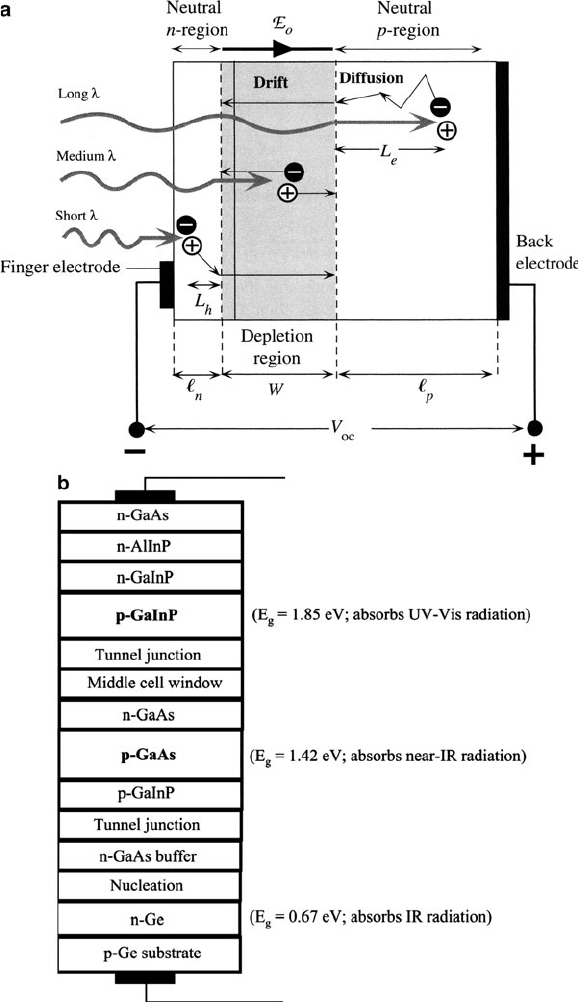
Figure 4.86. Schematic of (a) a single-junction and (b) multi-junction photovoltaic cell. The single-
junction cell is reproduced with permission from Kasap, S. O. Principles of Electronic Materials and
Devices, 3rd ed., McGraw-Hill: New York, 2007. Copyright 2007 The McGraw-Hill Companies.
336 4 Semiconductors
the depletion region or within a certain distance from this region (Figure 4.86a –
electrons within diffusion length L
e
, or holes within diffusion leng th L
h
) may
contribute to photocurrent. If the minority carriers are further away from the deple-
tion zone, recombination will occur rather than migration to their respective electro-
des (i.e., ele ctrons in n-Si flowing through the external circuit to neutralize the
excess holes in p-Si).
In the design of solar cells, a small bandgap semiconductor is desirable since
it requires less energy to promote electrons from valence to conduction bands.
However, though the resultant photovoltage of the solar cell is directly proportional
to the bandgap, higher energy photons would be converted to heat rather than
electrical energy. The use of a higher bandgap material would result in a lower
photocurrent since only high-energy photons (E E
g
) would be absorbed. The
bandgaps of Si and GaAs (1.1 eV (1,127 nm) and 1.4 eV (886 nm), respectively)
are able to absorb a broad range of electromagnetic radiation; however, the effi-
ciencies of Si or GaAs based solar cells are only 20–25%. Thin-film solar cel ls that
utilize amorphous silicon (a-Si) are also currently under investigation. Since Si
atoms do not form a continuous crystalline array, surface sites contain significant
numbers of dangling bonds, which are easily passivated through reaction with
hydrogen (yielding hydrogenated amorphous silicon, a-Si:H). The larger bandgap
of a-Si (1.7 eV) is more effective at capturing broadband solar energy; however, the
best efficiencies to date are less than 10% for this technology.
In order to capture a larger range of photon energies, multijunction photocells
have rece ntly been introduced. This method consists of a stack of semiconductor
layers with decreasing bandgaps (Figure 4.86b). Top layers have higher bandga ps,
and are able to absorb higher energy photons; lower layers of the cell absorb the
transmitted lower energy wavelengths. The multijunction solar cell shown in Fig-
ure 4.86b has resulted in an efficiency of 34%, the highest value reported for all
photovoltaic cells to date.
[101]
It has been proposed that replacement of GaAs with a
material with an E
g
of 1.25 eV would result in a higher overall efficiency, since more
photons would be collected by the second layer and fewer would be transmitted to
the bottom Ge substrate. With additional tweaking such as altering the number of
layers, individual layer thicknesses/stoichiometries, it is expec ted that multijunction
photocells with efficiencies of 45–50% and higher will soon be realized.
While it is important to control the stoichiometry of each layer to adjust their
bandgaps, it is equally important to have as few interfacial mismatches as possibl e.
That is, each layer must be epitaxially grown to ensure that the lattice constants are
perfectly matched. It has been shown that a lattice mismatch of only ca. 0.01% is
enough to cause significant electron-hole recombinations, resulting in lower cell
efficiency. CVD is the method of choice for the fabrication of these multilayer
devices; as you might expect, cells of this variety are relatively quite expensive.
In an effort to decrease the cost of productio n for solar cells, new architectures
known as dye-sensitized solar cells (DSC) are of increasing interest.
[102]
Instead of
light being absorbed by inorganic semiconductor laye rs, absorption occurs in an
organic-based film that comprises light-harvesting dye molecules bound to a TiO
2
4.4. Thermoelectric (TE) Materials 337