Gupta D. (Ed.). Diffusion Processes in Advanced Technological Materials
Подождите немного. Документ загружается.


various types have been placed as APDBs between two reacting films.
During the early years of the microelectronics era (the 1960s and early
1970s), gold-beam leaded interconnection technology led to very reliable
devices and circuits.
[3]
In this technology, the interconnections to the out-
side world were made by using Au, Pd, or sometimes a bilayer of Ti and
Pd between the Au and Si contacts. Contacts to Si were made using a sili-
cide of Pd or Pt, although some work was reported on the use of electro-
less- plated Ni.
[4]
Au could not be used directly on Si because of (1) its very
high diffusivity in Si, (2) its inability to bond with SiO
2
, which is always
present as a native oxide layer on the surface of silicon, and (3) the exis-
tence of a low temperature (370°C) eutectic in the Au-Si system.
[5]
Adirect
extension of the gold-beam leaded technology, when Al was introduced as
the contact to Si, was not possible because of the metallurgical interactions
between Al and Au and between Al and Pd. Such interactions, occurring at
relatively low temperatures, made the metallization mechanically and elec-
trically unstable. Asuitable barrier was needed. Ti/Pt bilayer and Ti/TiN/Pt
trilayer APDBs were found to satisfy this need and to be reliable under
actual fabrication and use conditions.
[6]
Note that a study of the thermody-
namics of the metal system (individual metals and their reaction products),
appropriate phase diagrams, and interdiffusion was essential for making
the right choice of the APDB between Al and Au. The need for an effective
Ti-Pt diffusion barrier between Al and Au, with a thickness of at least 200
nm of each individual metal, was recognized.
[6]
To investigate their relative
effectiveness as diffusion barriers, several two-metal, three-metal, four-
metal, and five-metal layers were fabricated and tested for interdiffusion,
failures, and preventing a reaction between Al and Au.
Interaction between two materials is a result of fast interdiffusion. In
thin films, a large number of fast diffusion mechanisms are operating,
leading to an obvious suggestion to use high-melting-point metals/alloys.
For diffusion through a lattice (so-called lattice diffusion), the self-diffusion
coefficient D
self
is indirectly related to the melting point (T
m
) of the mate-
rial by an empirical relation between the activation energy (Q
self
) of self-
diffusion and the melting point:
Q
self
34 T
m
, (2)
where T
m
is given in degrees Kelvin and Q
self
is given in calories per mole.
In most cases, D and Q are related through the Arrhenius relationship:
D D
o
exp(QRT), (3)
where R is the gas constant. Thus the higher the melting point, the higher
the activation energy and the lower the self-diffusion coefficient. However,
242 DIFFUSION PROCESSES IN ADVANCED TECHNOLOGICAL MATERIALS
Ch_05.qxd 11/29/04 6:19 PM Page 242

DIFFUSION BARRIERS IN SEMICONDUCTOR DEVICES, MURARKA 243
in thin films, which are generally deposited by vapor deposition techniques,
the diffusion is dominated by the grain boundaries. For self-diffusion
through grain boundaries, we can approximate the activation energy to be
about half that for the lattice diffusion given by Eq. (2). Thus, most thin-
film interactions are the result of grain boundary diffusion and other fast
diffusion paths, such as dislocations. If these fast diffusion paths can some-
how be blocked (or stuffed
[2]
), the interaction rate can be significantly
reduced. These relationships provided the concept of using refractory met-
als with stuffed grain boundaries for application as APDB thin films and
led to the use of W, Ta, Nb, Mo, Hf, Zr, V, Cr, and Ti metals. The electri-
cally conducting nitrides, carbides, and borides of these metals have very
high melting points. In early applications, these materials were suggested
as APDBs, and some were used, not only because they have high melting
points, but because the presence of a slight excess of the nitrogen, carbon,
and boron, respectively, in these materials stuffs the fast diffusion paths.
With decreasing device size in microelectronics (which caused
decreasing junction widths and depths, leading to the concern about the
use of Al contacts on Si) of the late 1970s and early 1980s, a diffusion bar-
rier was needed between Al and Si. The most commonly suggested barri-
ers (which have one common factor common: the high melting point)
have been the following:
1. Silicides
2. Refractory nitrides, carbides, or borides
3. Ti-W alloy
4. Refractory metal-noble (or near noble) metal alloy
5. A refractory metal alone
The most commonly used barriers between Al and Si have been the Ti-W
alloy, TiSi
2
TiN, TiSi
2
WTiTiN, CoSi
2
TiN, CoSi
2
TiTiN, W, and
WTiN. In most advanced Si integrated circuits, a CoSi
2
TiTiNW thin-
film structure is used in the Al or Cu interconnect technology.Unlike the
Al interconnects on SiO
2
, which do not require any APDB material due to
their natural adhesion property without interdiffusion, APDB material is
needed between Cu and SiO
2
. This has led to a renewed search. Presently,
a nitride of Ta (TaNx) is being used between SiO
2
and Cu, and between W
(in the contact windows) and Cu.
[7]
The barrier thickness is in the range of
5 to 30 nm, and the resistivity is high (200 to 300 mΩ cm). For future
applications, either the thickness has to be reduced by an order of
magnitude or the resistivity of the barrier has to be similar to that of Cu.
These requirements have led to a flurry of activities in self-forming
barriers/adhesion promoters
[8]
and in a newer group of materials called
self-assembled molecules (SAMs)
[9]
in which a monolayer of molecules,
Ch_05.qxd 11/29/04 6:19 PM Page 243

generally about 1 nm thick, is formed on a given surface and could act as
an APDB layer between the ILD and Cu. In the future, a lower dielectric
constant (k) interlayer dielectric (ILD) film,
[10]
which may be a polymer,
fluorinated/carbonated SiO
2
, or a porous material, may replace pure SiO
2
as an ILD. Such replacements may also place new constraints on the prop-
erties of APDB materials. These new concepts and their applications are
reviewed in Sec. 5.6.
5.3 Brief Review of Diffusion and the
Influencing Material Factors
5.3.1 Diffusion in the Lattice and Grain Boundaries
Equation (1) simply states that the rate of transfer of a diffusing
species across a unit area perpendicular to the x direction is proportional
to the concentration gradient in that direction. If we consider diffusion
across an element of volume and use the law of conservation of matter, we
reach a conclusion that the rate at which the concentration changes in this
volume must equal the local decrease of the diffusion flux, leading to the
one-dimensional Fick’s second law of diffusion:
∂c(x, t)∂t ∂{D [∂c(x, t)∂x]}∂x. (3)
For concentration-independent D, Eq. (3) simplifies to:
∂c(x, t)∂t D [∂
2
c(x, t)∂x
2
]. (4)
To determine D, we must carefully determine the concentration of the
diffusing species as a function of the depth in the sample for a given dif-
fusion treatment (that is, time, temperature, and ambient). Equation (3)
or (4) is then solved using the experimentally placed boundary condi-
tions. Avariety of solutions fitting various boundary conditions are avail-
able.
[11]
Two of the most commonly used solutions of Eq. (4) are Gaussian
and error-function distributions given, respectively, by the following
equations:
c(x, t) M√(pDt) exp(x
2
4Dt) (5)
and
c(x, t) c
s
erfc[x2√(Dt)]. (6)
244 DIFFUSION PROCESSES IN ADVANCED TECHNOLOGICAL MATERIALS
Ch_05.qxd 11/29/04 6:19 PM Page 244

DIFFUSION BARRIERS IN SEMICONDUCTOR DEVICES, MURARKA 245
Here M is the total amount of the diffusing substance that is constant, c
s
is the time-independent surface concentration of the diffusing species,
and erfc is the complimentary error function related to the error function
by:
erfc (z) 1 erf (z). (7)
Note that the solutions given by Eq. (5) or (6) are for concentration-
independent D and are useful in most cases of interest. For concentration-
dependent D, several solutions (and approximations) of Eq. (3) have been
examined and presented.
[11]
To obtain a reasonable estimate of the penetration by a diffusing
species, we can calculate the diffusion depth, x
D
, for a diffusion time t and
at a temperature for which a value of D has been obtained. Theoretically,
x
D
should be infinite, since x
D
will be determined by the condition c 0
at t 0. For most practical purposes, x
D
is defined as:
X
D
2
4Dt. (8)
Use of this definition to determine a typical diffusion depth simply indi-
cates that cc
s
has a predetermined value: for Gaussian solution (Eq. 5),
cc
s
1/e 0.37; for the error-function solution (Eq. 6,) cc
s
0.1573.
In this context, we also define the transport velocity, V(cm/sec),
across a material of thickness d, which is given by:
V Dd. (9)
Thus, to minimize the mass transport, Vshould be reduced by minimizing
D across the APDB and/or by increasing the thickness, d, of the APDB.
The latter is difficult to achieve, leaving the choice of selecting a very thin
film of APDB material with the lowest possible D of the impurity.
To use Eqs. (5) and (6) rigorously, diffusion measurements are gener-
ally made in the lattice of ideal solids that contain only point defects in
thermal equilibrium that provide energetically favored migration paths. In
real solids and especially in thin films, their microstructures become very
important and a large number of fast-diffusion paths, such as grain bound-
aries, surfaces, and dislocations, exist and contribute to enhancing the
low-temperature diffusion coefficient by several orders of magnitude. At
diffusion temperatures of less than half the melting point (in degrees
Kelvin), surface, grain boundary, and dislocation diffusion coefficients are
higher than the lattice diffusion coefficient by about 8, 7, and 5 orders of
magnitude, respectively.
[12]
We can derive relationships between J
gb
and J
L
that represent grain boundary and lattice fluxes, respectively, when diffusion
Ch_05.qxd 11/29/04 6:19 PM Page 245

from the grain boundary into the adjoining grains is permitted:
J
gb
J
L
2dD
gb
D
L
. (10)
D
gb
and D
L
are diffusion coefficients in the grain boundary and in the lat-
tice, respectively, and d is the grain boundary width. This relationship is
obtained by considering a situation in which the concentration on the front
and back surfaces of the slab of the polycrystalline material is maintained
constant, and a steady state is assumed because all concentration gradients
parallel to the plane of the slab are eliminated. Note that in these consid-
erations, grain boundaries offer unrestricted diffusion. Any segregation of
the diffusing species and others present in the films will seriously affect
both fluxes. Gupta et al.
[13]
have explained the solute (impurity) effect in
changing the diffusion of solvent atoms (for example, Al in an Al-Cu
alloy) phenomenologically. They considered interactions of the solute
(impurity) atoms with defects in the lattice, in the grain boundaries and
the equilibrium solute adsorption at the grain boundaries. The solute effect
on the grain boundary diffusivity has been shown to depend not only on
the associated solute-binding free-energy difference (∆G
a
) between the
grain boundary and the lattice sites, but also on the changes in the lattice
diffusion, as given by:
[(D
gbp
D
gba
) (D
La
D
Lp
]
12
1 c
o
exp(∆G
a
RT), (11)
where subscripts p and a refer to pure and alloyed metal, respectively, and
c
o
is the solute concentration in the lattice. For c
o
1, Eq. (11) predicts
diffusion enhancement at high temperatures and retardation at low
temperatures.
5.3.2 Interdiffusion Between Two or More
Materials in Contact
There are no universal models of diffusion/interdiffusion in thin films
of various materials in contact with each other. Balluffi and Blakeley
[14]
have examined the complexities in the details of diffusion processes in
thin films and point out the following:
“Diffusion in thin films may be expected to have special characteris-
tics for a number of reasons, which include the following: (1) thin films
are invariably diffused at relatively low temperatures because of their
poor thermal stability; (2) all volume elements are in close proximity to
either a free surface or interphase boundary of some kind; (3) films gen-
erally contain high densities of low-temperature short circuits for diffusion
246 DIFFUSION PROCESSES IN ADVANCED TECHNOLOGICAL MATERIALS
Ch_05.qxd 11/29/04 6:19 PM Page 246

DIFFUSION BARRIERS IN SEMICONDUCTOR DEVICES, MURARKA 247
such as grain boundaries and dislocations; (4) large biaxial stresses in the
plane of the film are often present; (5) relatively high concentration of
uncontrolled impurities may be present as a result of special fabrication or
diffusion conditions; (6) disordered or metastable structures may be present;
(7) diffusion often occurs over short distances under the influence of large
concentration or electrostatic potential gradients; and (8) steep-chemical
gradients and low temperature may affect the possible maintenance of
local equilibrium at phase boundaries during multiphase diffusion.”
It is then expected that at the typical post-metal-anneal temperatures
of 300 to 450°C, grain boundary diffusion will dominate in films of the
high-melting-point metals of interest, that is, Ti, Ta, Pt, W, metallic sili-
cides, and the refractory nitrides, carbides, and borides. On the other hand,
in metals such as Al and Mg, lattice diffusion will dominate at the same
temperatures. Diffusion behavior in copper is somewhere in between. In
developing an APDB film, our goal is therefore to eliminate or minimize
the interaction or reaction between materials of interest and the APDB
film. The reactivity can generally be estimated by evaluating the interdif-
fusion coefficients in thin films. Interdiffusion coefficients are strongly
related to the microstructure of these films; the mutual solid solubilities;
the intermetallic or compound formation, as suggested by the phase dia-
grams; the free energies or heats of fomation of these intermetallics and
compounds; and the temperature. For the devices/circuits in use, the ILDs
sandwiched between two interconnect layers are exposed to very high
electric fields (of the order of 1 MV/cm), which causes diffusion of metal
ions into the ILD. Thus, an APDB material is required between the metal
and the ILD.
The interdiffusion coefficient (D
ij
) reflects the average overall move-
ment of both constituents, say, i and j (representing two solids in contact),
diffusing in a concentration gradient. For an ideal case of a binary sys-
tem, D
ij
is given in terms of the individual diffusion coefficients, D
i
and
D
j
, and their respective concentrations, c
i
and c
j
, in the diffused alloy at
a depth x:
D
ij
(x) D
i
c
j
(x) D
j
c
i
(x). (12)
D
ij
is then used to replace D in Eq. (3) or (4). In thin-film interactions,
invariably, D
ij
is obtained even when the binary system does not form the
ideal solid solution. Also in such cases, because of the lack of crystallinity,
the experimentally determined D
ij
is an averaged grain boundary interdif-
fusion coeficient, at best. For the interaction between an APDB film and
another film in contact, D
ij
must be negligibly small or the thickness of
the barrier film large so that the reaction does not reach the other
surface/interface.
Ch_05.qxd 11/29/04 6:19 PM Page 247

5.3.3 Role of Material Properties
Controlled Microstructure
Barrett et al. have stated:
[15]
“Practically all the useful properties of
materials are strongly dependent on their internal structure,” and “for a
material of given chemical composition, the internal structure is not con-
stant.” The effect of the internal structure or microstructure on the bulk
properties of materials is known. The microstructure of thin-film inter-
connections plays a very important role in determining two important
reliability factors: (1) the reactivity with the surroundings, and (2) the
electromigration and stress voiding.
As mentioned in Sec. 5.3.1, real materials are used for metallization
applications such as thin films of copper. Information on the lattice
parameter, density, and so forth for Cu can be readily found in handbooks.
All defects are extremely important in thin films. Chemical reactivity,
atomic diffusion, and electrical and mechanical properties are affected by
the presence of defects. Also, the properties of the materials are not
isotropic and depend on a specific crystallographic direction under con-
sideration. For example, in the face-centered cubic Al or Cu, (111) planes
have the highest density of atoms with low energy, and therefore behave
differently than (100) planes. For bulk polycrystalline metal with random
texture, isotropic behavior is obtained when the individual cystallites are
oriented throughout space with equal directional probability. The effective
macroscopic properties can be calculated by considering the directionally
dependent values averaged over all orientations in space.
For bulk material, especially the metals, the practical ways to con-
trol the microstructures to yield the desired and useful properties are
well known to metallurgists and materials scientists. The concepts are
also important for thin films to be used as APDB, but are difficult, if not
impossible, to be realized. Preparation of the substrate surfaces, surface
forces, and deposition methods, and the attendant parameters, yield a
microstructure variability that is not well understood. It is well known
that the substrate-film interface, the film surface (which may be covered
by a native oxide or other compounds), the impurities that segregate at
defect sites, and the grain boundaries are effective barriers to the motion
of dislocations, thus affecting both the film strength and film
microstructure. In Al and Cu thin films, texturing leads to deviation
from the isotropic polycrystalline thin-film case. Texture is defined as
the tendency of the individual crystallites of a material to acquire a pre-
ferred crystallographic orientation. The texture affects materials properties,
and thus affects performance. For example, the texture of electroless
copper film has been shown to affect the resulting oxidation behavior.
[16]
248 DIFFUSION PROCESSES IN ADVANCED TECHNOLOGICAL MATERIALS
Ch_05.qxd 11/29/04 6:19 PM Page 248

DIFFUSION BARRIERS IN SEMICONDUCTOR DEVICES, MURARKA 249
The correlation of room-temperature stress with texture and the subse-
quent influence on film resistivity have also been noted.
[17]
A recent
review discussed the observed texture responses of copper thin films
deposited by a variety of techniques.
[18]
In general, (111), (200), and
random components of texture dominate the response, although in
some cases, (220) and (520) texture components have been observed.
From surface energy considerations, the close-packed (111) oriented
grains should be favored. Frequent occurrence of an extensive fraction
of the (200) texture, which has been found the most stable, is not well
understood.
Texturing and microstructure are affected by thermal treatments, after
or during deposition, and are influenced considerably by the annealing
ambient. In certain cases, thermal annealing of copper films is found to
induce the formation of giant grains.
[19, 20]
The strain energy has been sus-
pected of playing a role in this regard.
Impurities significantly influence the microstructural evolution due to
(1) diffusion in and out of grain boundaries, (2) interaction with the host
metal, and (3) segregation in grain boundaries and dislocations, and at
surfaces and interfaces. Impurity fluxes in the grain boundaries have con-
tributed to grain boundary motion
[21]
and diffusion-induced recrystalliza-
tion,
[22]
and thus to grain growth. On the other hand, impurity segregation
at the grain boundaries and other short-circuiting paths such as disloca-
tions, surfaces, and interfaces is known to suppress the diffusion in or on
the material. Solute segregation at the grain boundaries and interfaces is
discussed later in this section. The lower the solid solubility is in the grain,
the higher the concentration is in the grain boundary.
[23]
For example, the
segregation of Cu in the grain boundaries of Al, either as metallic Cu or
as a Cu-Al alloy, leads to a retardation of the Al migration caused by the
imposed electric field (that is, electromigration is retarded, leading to
improved mean time to failure). Grain boundary stuffing has been known
to produce effective thin-film diffusion barriers.
[2]
The effect of Mg or Al
added to Cu, in concentrations less than the solid solubility limit, on the
microstructure has been investigated to reveal the metallurgical variables
of the APDB effectiveness of these alloys used between Cu and SiO
2
.
[24, 25]
The effectiveness of Mg or Al is attributed to their thermodynamically
favorable abilities to reduce SiO
2
, leading to the formation of an interfa-
cial layer, between Cu and SiO
2
, that acts as an APDB layer. The
microstructures of annealed Cu, Cu-Al, and Cu-Mg structures, however,
show very different behaviors. Pure copper has moderate to heavy twin-
ning with relatively uniform microstructure. Cu-Al has a clear bimodal
distribution of small (∼25 nm) and large (∼160 nm) grains and heavy twin-
ning. Cu-Mg, like pure Cu, shows a bimodal microstructure with consid-
erably less twinning.
Ch_05.qxd 11/29/04 6:19 PM Page 249

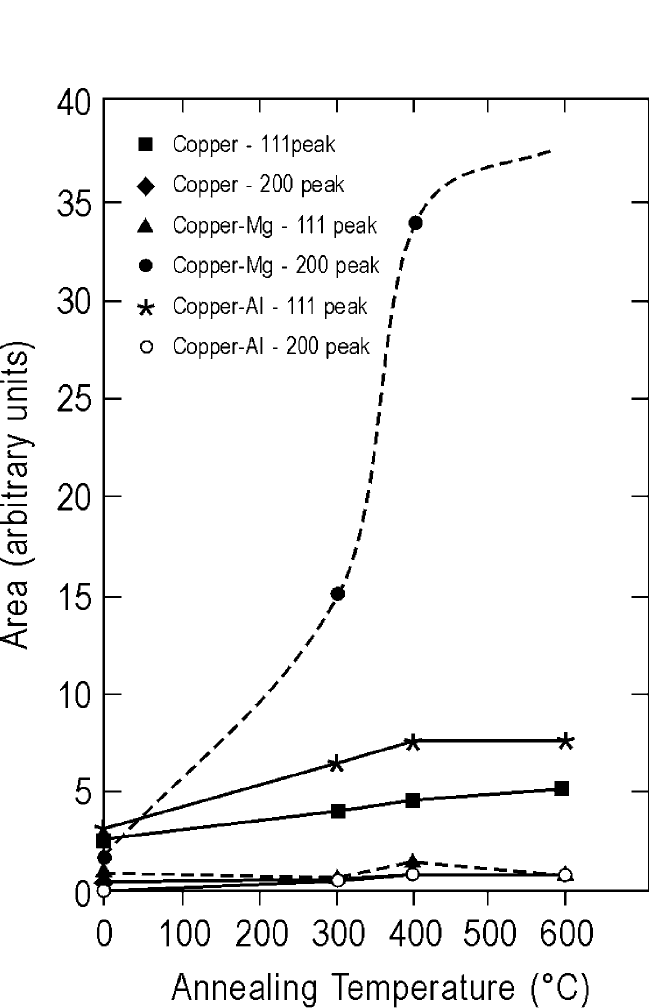
Figure 5.1 compares the (111) and (200) x-ray diffraction peak inte-
grated intensities of three films as a function of annealing temperature. Cu
and Cu-Al films have a preferred texture [with (111) to (200) ratio in
annealed films as high as 15] that agrees with the observed twinning typ-
ical of (111) orientations. Cu-Mg shows a complete reversal of preferred
texture, with (200) stronger than (111) [a (111) to (200) ratio of 0.04 after
400°C and 0.01 after 600°C anneal]. Temperature also has a large influ-
ence on the growth of (200) texture compared to that of (111). It is appar-
ent that there is a remarkable difference in the behavior of Al and Mg
alloying elements in controlling the microstructure of Cu films, especially
when the added impurity concentrations are below the solid solubility
limit. These differences could have a large impact on the diffusion in the
metal and thus on the electromigration behavior.
Note that in the case of Al metal, the measured mean time to failure
for the electromigration was found to increase with the increasing grain
size and the degree of (111)-preferred orientation; decreasing the spread
of grain size distribution is beneficial.
[26]
Electron microscopic studies of
the narrow lines have shown that the grain structure takes on a so-called
bamboo appearance, with grain boundaries generally running perpendicu-
lar to the direction of the current flow (that is, along the interconnection
length).
[27]
Similarly, the superiority of the Al-Cu alloys
[28]
and of e-gun
evaporated metals or alloys is associated with the resulting preferred (111)
texture and uniform grain size distribution.
Mutual Solid Solubilities and the Phase Diagrams
Solid solubilities of i into j and of j into i play an important role in
determining the outcome of the reaction between i and j. If the solid sol-
ubilities are large, the interdiffusion leads to a solid solution prior to for-
mation of any compound. For example, titanium can dissolve significant
amounts of oxygen prior to the oxide formation. The advantage of such a
system is that no new phase appears in early periods of reaction. On the
other hand, when the mutual solid solubilities are low, compound forma-
tion occurs immediately. For example, oxides of W form readily because
W does not dissolve any significant amount of oxygen. In the absence of
a compound formation, second-phase (i or j) precipitation has been seen
on cooling from high temperatures where solid solubilities were higher.
For example, aluminum dissolves larger amounts of silicon at 450°C, the
typical metal anneal temperature. On cooling to room temperature, silicon
precipitates out as the second phase in aluminum film and at the silicon-
aluminum interface. Solid solubility does play a role in the second-phase
formation, but it does not play a direct role in influencing the diffusion
250 DIFFUSION PROCESSES IN ADVANCED TECHNOLOGICAL MATERIALS
Ch_05.qxd 11/29/04 6:19 PM Page 250
DIFFUSION BARRIERS IN SEMICONDUCTOR DEVICES, MURARKA 251
Figure 5.1 Area under x-ray diffraction peak vs.annealing temperature of Cu and
Cu alloys. All annealing times were 30 minutes except annealing done at 600°C,
which lasted 120 minutes.
Ch_05.qxd 11/29/04 6:19 PM Page 251