Henini M. Handbook of Self Assembled Semiconductor Nanostructures for Novel devices in Photonics and Electronics
Подождите немного. Документ загружается.

Slow Oscillation and Random Fluctuation in Quantum Dots: Can we Overcome? 389
having separation in the transverse direction comparable to the QD size, and coupling in the transverse
direction, may be enhanced by electron occupation forming “ molecular bonds ” , resulting a 2D sheet.
Spreading the transverse momentum means having the incident electron at an angle, which is
more affected by interface roughness and trapping sites. In classical systems, individual contri-
butions without phase differences are simply summed. In waves, phase differences of individual
entities produce interference and possible instabilities. Therefore inhomogeneity in QDs magnifi es
problem in QWs. Using common sense, a parallel system is more subjected to instability caused
by localized deviations. I conclude after many years of thinking about the problem of quantum
electronic devices, that our saviour is the tolerance brought by the introduction of phase rand-
omization in a large N-body coupled system that overwhelms the “ devil ” , Pauli’s exclusion prin-
ciple. Too bad that electrons, mainly because of their charge, cannot be allowed in the same state
as Bosons.
0
40
50
(a)
(b)
(c)
60
70
80
90
42
0 20 40 60 80 100 120 140
43
100 200 300 400
Time (s)
3*P
3*P
2*P
P
Intensity (lin. scale)
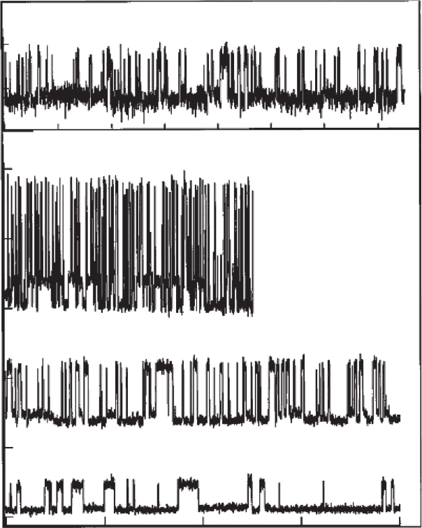
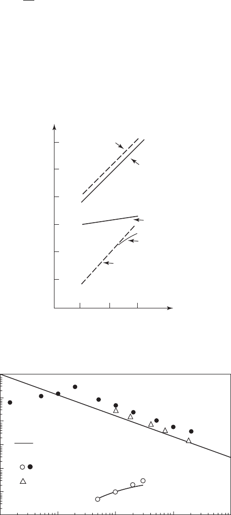
Figure 12.22 Telegraph switching of InP in Ga
x
In
1
x
P: (a) low excitation – switching between two levels; (b) high
excitation – switching between three levels; (c) after partial quenching [33] .
CH012-I046325.indd 389CH012-I046325.indd 389 6/24/2008 3:37:25 PM6/24/2008 3:37:25 PM
390 Handbook of Self Assembled Semiconductor Nanostructures for Novel Devices in Photonics and Electronics
12.8 Summary
Let us look more closely at conductance consisting of delta function-like peaks and steps, as a
function of the applied voltage. Whenever the fi rst jump in conductance involves two electrons,
our data are more predictable, whereas the fi rst jump involves only one electron, it is more com-
mon to observe telegraph-like G–V. This fact indicates that a defect traps an electron and holds
onto it by drastically changing the potential and blocking other electrons. Except in SK QDs, I am
inclined to think that QDs in general have more defects than QWs simply because the surface vol-
ume ratio in QDs is much higher than in QWs. Second, the state in a nanoscale QD is similar to a
defect. After we discovered the effects from light, we realized that the process seems to be caused
by a variety of trappings, although the data did not rule out trapping from non-conducting
dots, instead of some unknown defects. The main many-body effects can be lumped into one,
the Coulomb term normally taken as a small perturbation in atomic and even solid-state phys-
ics. There is no doubt in my mind that some sort of general usage of QDs will be found and developed.
However, I also predict that nanoelectronics will never be developed in computers. I have mentioned that
living organism utilize ions instead of electrons. The ratio of weight between a sodium atom and elec-
trons is the same as that between a 200 kg lead ball and a ping pong ball. This is why nature, with a few
hundred millions of years of evolution, perfected the ionic instead of electronic system, in what may be
called the single ion transistor.
Acknowledgements
I take this opportunity to acknowledge our original funding from NSF, followed by ONR, ARO and
DARPA. Most of all thanks go to my students J. Clay Lofgren, Daniel Boeringer, Xiaolei Li, Amanda
Bowhill, Jonder Morais, Chen Ding, Quiyi Ye and my colleague the late E.H. Nicollian.
References
1. L. Esaki and R. Tsu , IBM Res. Develop. 14 , 61 ( 1970 ) .
2. R. Tsu and L. Esaki , Appl. Phys. Lett. 22 , 562 ( 1973 ) .
3. L.L. Chang , L. Esaki , and R. Tsu , Appl. Phys. Lett. 24 , 593 ( 1974 ) .
4. R. Tsu , Q.-Y. Ye , and E.H. Nicollian , SPIE 1361 , 232 ( 1990 ) . Q.-Y. Ye, R. Tsu, and
E.H., Nicollian, Phys. Rev. B. 44 , 1806 (1991).
5. R. Tsu , X.-L. Li , and E.H. Nicollian , Appl. Phys. Lett. 65 , 842 ( 1994 ) .
6. D. Bertram , M.C. Hanna , and A.J. Nosik , Appl. Phys. Lett. 74 , 2666 ( 1999 ) .
7. J.D. Joannopoulos , R.D. Meade , and J.N. Winn . Photonic Crystals ( Princeton U Press, 1995 ) .
8. K. Liu , T.A. Schmedake , K. Daneshvar , and R. Tsu, Microelectronic J. (2007 ) .
9 . R . T s u , Nanotechnology 12 , 1 ( 2001 ) .
10. D. Babic , R. Tsu , and R.F. Greene , Phys. Rev. B. 45 , 14150 ( 1992 ) .
11. R. Tsu , D. Babic , and L. Ioriatti , J. Appl. Phys. 82 , 1327 ( 1997 ) .
12. R. Tsu and D. Babic , Appl. Phys. Lett. 64 , 1806 ( 1994 ) .
13a. J. Zhu , T.J. LaFave , and R. Tsu , Microelectronic J. 37 , 1296 ( 2006 ) .
13b. T.J. LaFave and R. Tsu to be published.
14. R. Tsu , SPIE 1361 , 313 ( 1990 ) .
15. R. Tsu . Superlattice to Nanoelectronics , ( Elsevier , Amsterdam , 2005 ) .
16. R. Tsu , J.G. Hernandez , S.S. Chow , and D. Martin , Appl. Phys. Lett. 4 8 , 647 ( 1986 ) .
17. R. Tsu , Physica B. 189 , 235 ( 1993 ) where additional trap-charge is included .
18. R. Tsu , Microelectronics J. 34 , 329 ( 2003 ) .
19. X.-L. Li (1993) MS thesis, Department of Electrical Engineering, UNC-Charlotte.
20. C. Ding (1994) MS thesis, ECE, UNCC.
21. C. Ding and R. Tsu , Mat. Res. Soc. Symp. Proc. 378 , 757 – 760 ( 1995 ) .
22. K.R. Farmer , R. Saletti , and R.A. Buhrman , Appl. Phys. Lett. 52 , 1749 ( 1988 ) .
CH012-I046325.indd 390CH012-I046325.indd 390 6/24/2008 3:37:26 PM6/24/2008 3:37:26 PM
Slow Oscillation and Random Fluctuation in Quantum Dots: Can we Overcome? 391
23. K.K. Likharev , IBM J. Res. Dev. 32 , 114 ( 1988 ) .
24. M.W. Dellow , P.H. Beton , C.J.G.M. Langerak , T.J. Foster , P.C. Main , L. Eaves , M. Henini ,
S.P. Beaumont , and C.D.W. Wilkinson , Phys. Rev. Lett. 6 8 , 1754 ( 1992 ) .
25. X.L. Li (1994), MS thesis, unpublished, UNC-Charlotte.
26. R. Tsu, Microelectronic J. 39, 335 (2008).
27. K. Liu, T.A. Schmedake, K. Daneshvar, and R. Tsu, Microelectronic J. 38, 700 (2007).
28. E. Moskalenko , K.F. Karlsson , T. Donchev , P.O. Holtz , B. Monemar , W. Shoenfeld , and P.M. Petroff ,
Nano Lett. 5 , 2118 ( 2005 ) .
29. K.F. Karlsson , E. Moskalenko , P.O. Holtz , B. Monemar , W.V. Shoenfeld , J.M. Garcia , and
P.M. Petroff , Appl. Phys. Lett. 78 , 2952 ( 2001 ) .
30. M. Nirmal , B.O. Dabbousi , M.G. Bawendi , J.J. Macklin , J.K. Trautman , T.D. Harris , and L.E. Brus ,
Nature 383 , 803 ( 1996 ) .
31. P. Castrillo , D. Hessman , M.E. Pisto , J.A. Prieto , C. Pryor , and L. Samuelson , Jpn. J. Appl. Phys. Part 1.
36 , 4188 ( 1997 ) .
32. M.J. Kirton and M.J. Uren , Adv. In Physics 38 , 367 ( 1989 ) .
33. M.-E. Pisto , Phys. Rev. B. 63 , 113301 –1 ( 2001 ) .
CH012-I046325.indd 391CH012-I046325.indd 391 6/24/2008 3:37:26 PM6/24/2008 3:37:26 PM
Radiation Effects in Quantum Dot Structures
Nikolai A. Sobolev
I3N-Institute for Nanostructures, Nanomodelling and Nanomanufacturing, and
Departamento de Física, Universidade de Aveiro, 3810-193 Aveiro, Portugal
13.1 Introduction
The tolerance of materials and devices to radiation-induced defects (radiation defects, RDs) is of
crucial importance in atomic energy and space applications. In a nuclear reactor, the samples are
exposed to neutrons and gamma-quanta. The space-radiation environment accompanying most
useful orbits consists of energetic electrons (energies up to ⬃ 7 MeV), protons (energies extending
to hundreds of MeV) and small amounts of low energy heavy ions [1] . The predicted proton and
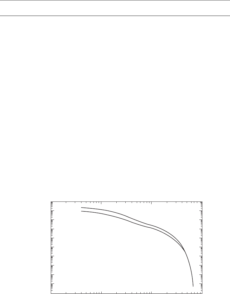
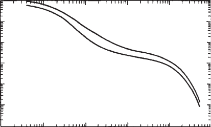
electron fl uxes for low earth orbit (LEO) missions are presented in Figs 13.1 and 13.2 . The LEO
proton spectrum is especially hard: between 50 and 500 MeV the proton fl ux decreases only by a
factor of 4.
Furthermore, the creation of RDs is an inevitable collateral effect in ion implantation that is a
well-established technique of materials modifi cation. Finally, there is a possibility of using RDs
CHAPTER 13
10
11
10
10
10
9
10
8
10
7
10
6
10
5
10
4
10
3
10
2
10
1
10
2
10
1
10
0
10
1
Energy (MeV)
Daily electron fluxes
(AE8)
Orbit: 60°/500 km
New method 1
Solar max
Averaged integral electron flux
(#/cm
2
·day)
S
o
l
a
r
m
i
n
Composite LEO orbit spectra
Figure 13.1 Low earth orbit (LEO) proton fl uxes [1] .
CH013-I046325.indd 392CH013-I046325.indd 392 6/24/2008 3:45:27 PM6/24/2008 3:45:27 PM
Radiation Effects in Quantum Dot Structures 393
themselves in the device technology. With the onrushing advent of quantum-size semiconductor
structures (QSSS), the studies of RDs in them rapidly grow in importance.
Before discussing the physics of the interaction of radiation with matter, it is worth comment-
ing on the terminology. The energy absorbed by a specimen per mass unit is dubbed dose and is
measured in Gray (Gy J · k g
1
). One Gy is equal to 100 rad. The fl ux is the number of particles
passing during 1 s through a 1 m
2
area (m
2
· s
1
) ; integrating over time gives the fl uence meas-
ured in m
2
. It has to be noted that physicists often confuse the terminology in their publications,
calling dose what in reality is fl uence and measuring it, for convenience, in cm
2
.
The result of irradiating a semiconductor material will depend on the type of radiation, its
mode (pulsed, continuous) and type of interaction with the material, as well as the type of mate-
rial. The two main types of interaction of radiation with materials are atomic displacements and
ionization. All particles (electrons, protons, heavy ions and photons ranging from UV to gamma
energies) except neutrons produce ionization effects in materials. Besides, the radiation effects in
solid-state devices include single-event upsets.
When an energetic ion penetrates a material, it loses energy mainly by two nearly independent
processes: (i) elastic collisions with the nuclei known as nuclear energy loss (d E /d x )
n
, which dom-
inates at an energy of about 1 keV/amu; and (ii) inelastic collisions of the highly charged projec-
tile ion with the atomic electrons of the matter known as electronic energy loss (d E /d x )
e
, which
dominates at an energy of about 1 MeV/amu or more. In the inelastic collision (cross-section
⬃ 10
1 6
c m
2
) the energy is transferred from the projectile to the atoms through excitation and
ionization of the surrounding electrons. The amount of electronic loss in each collision varies
from tens of eV to a few keV per Å [2] .
The atomic displacements occur due to the transfer of momentum of the incident particle to
the atoms of the target material (nuclear energy loss). Provided an atom subjected to such a col-
lision receives suffi cient kinetic energy, it will be removed from its position and leave behind a
vacancy. The removed atom may meet another such vacancy and recombine or lodge in an inter-
stitial position in the lattice (a self-interstitial) or be trapped by an impurity atom. The vacancies
may be mobile, too, and either combine with impurity atoms or/and cluster with other vacan-
cies. Defects that are stable at the irradiation temperature may become mobile upon subsequent
heating. For the evaluation of the radiation damage in solids the mobility of the defects is of par-
amount importance. The self-interstitials in silicon are mobile even at 0.5 K [3] . In semiconduc-
tors such as Si, Ge, GaAs, GaSb, InP, InAs, AlAs, and InSb a large part of the primary defects
undergoes annihilation even below room temperature (RT). The RDs in these materials, which
are found at RT, consist mainly of secondary and tertiary complexes formed by migration and
agglomeration of vacancies and interstitials with each other and with impurities. The resulting
complexes are usually electronically active.
10
9
10
8
10
7
10
6
10
5
10
4
10
3
Averaged integral proton flux
(#/cm
2
·day)
Composite LEO orbit spectra
S
o
l
a
r
m
a
x
S
o
l
a
r
m
i
n
Daily proton fluxes (AP8)
Orbit: 60°/500 km
New method 1
10
2
10
1
10
0
10
1
10
2
10
3
Energy (MeV)
Figure 13.2 Low earth orbit (LEO) electron fl uxes [1] .
CH013-I046325.indd 393CH013-I046325.indd 393 6/24/2008 3:45:28 PM6/24/2008 3:45:28 PM
394 Handbook of Self Assembled Semiconductor Nanostructures for Novel Devices in Photonics and Electronics
When the energy of the primary recoil atom is high, which is especially the case upon ion
implantation or neutron irradiation, a collision cascade develops, where the defect density is much
higher than upon electron or proton irradiation. This high defect density may lead to an amor-
phization of the implanted layer. The accompanying defect rearrangement processes are usually
quite complex and not yet understood in all details even in elemental semiconductors such as Si.
The fundamentals of the radiation defect creation in solids can be briefl y described as follows
[4] . The total cross-section for the displacement of an atom from its regular lattice site as a result
of an elastic collision is given by:
σσ() d(,)EET
T
d
T
m
∫
(13.1)
where E is the kinetic energy of the incident particle, T is the kinetic energy transmitted to the
lattice atom, and d σ ( E , T ) is the differential cross-section of the corresponding interaction. The
integration is performed over the energy T from the minimum energy T
d
necessary for the dis-
placement of a lattice atom into an interstitial position to the maximum energy T
m
that the
incident particle can transmit to the target atom. The energy T
d
is called threshold energy. The
differential cross-section depends on the interaction potential. In the case of charged particles
(electrons, protons, ions) the interaction can be described by the Coulomb potential; for the neu-
tral particles (neutrons) it is rather similar to the collision of hard spheres. Usually the threshold
energy is taken as isotropic, because it is diffi cult to observe an appreciable orientation depend-
ence of T
d
in the experiment. The experimental values of T
d
for various semiconductor materials
are given in Table 13.1 [4, 5] .
Table 13.1 Experimental threshold energy values for the
atomic displacement damage for various semiconductors
(data taken from [4, 5] ).
Crystal T
d
, eV Crystal T
d
, eV
Diamond 35 5 InSb 6.4–9.9
Si 21 InAs 6.7–8.3
Ge 27.5 GaSb 6.2–7.5
GaAs 7–11 InP 3–4 (In) 8 (P)
To calculate the number of displacements produced by an incident particle, one has to solve
the integral in Eq. (13.1), taking into account the type of interaction.
For heavy charged particles, the value of d σ ( E , T ) is given by the Rutherford formula, and the
result of the integration is:
σ()E
TT
dm
a
11
⎛
⎝
⎜
⎜
⎜
⎜
⎞
⎠
⎟
⎟
⎟
⎟
(13.2)
with
a
ZZe
E
M
M
π
1
2
2
24
1
2
.
(13.3)
The index 1 designates the incident particle and 2 belongs to the target atom.
For neutron irradiation, the hard spheres collision model may be adopted, so that one obtains:
d( )
d
σπRR
T
T
m
12
2
(13.4)
CH013-I046325.indd 394CH013-I046325.indd 394 6/24/2008 3:45:28 PM6/24/2008 3:45:28 PM
Radiation Effects in Quantum Dot Structures 395
where R
1
and R
2
are the radii of the incident particle and the target atom, respectively. Taking
into account that M
1
M
2
, the result is:
σπ() ( ) .ERR
T
T
d
m
12
2
1
⎛
⎝
⎜
⎜
⎜
⎜
⎞
⎠
⎟
⎟
⎟
⎟
(13.5)
For the electrons with MeV energies, the Rutherford formula has to include relativistic correc-
tions. The exact calculation has been performed by N. Mott [6] ; an approximate solution has
been obtained by McKinley and Feshbach [7] . However, even the latter formula is relatively
sophisticated.
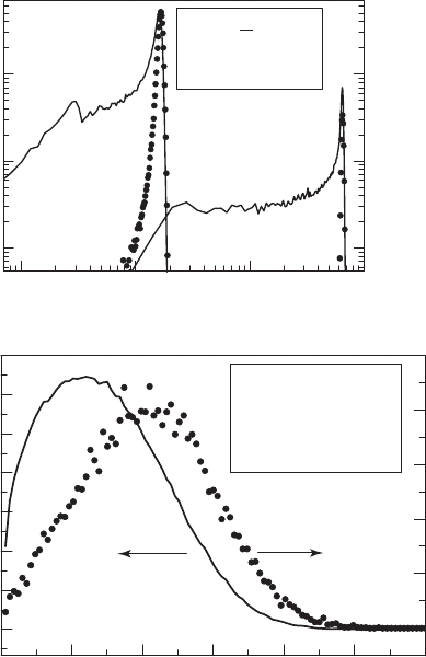
Figure 13.3 gives an idea of the energy transferred by an incident particle to the target atoms
as a function of the energy for electrons, protons and neutrons [4] . Note that collisions with neu-
trons are much harder in terms of the average energy transmitted to a target atom than those
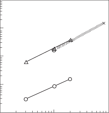
with protons of equal energy. In Fig. 13.4 a comparison of experimental damage coeffi cients in
10
5
10
4
10
3
10
1
10
1
1
10
2
Transmitted energy (eV)
10 100 1000
Incident energy (keV)
n,p
n
p
e
e
Figure 13.3 Maximum (dashed line) and average (full line) energy transmitted to a silicon atom as a function of
the incident energy for electrons (e), protons (p), and neutrons (n). [4]
Proton
InP
100000
10000
1000
100
10
1
0.1
0.10.01 10 1001
Energy of electrons and protons (MeV)
Calculated values
Relative damage coefficient
Experimental values
Solar cell data
DLTS data
Electron
Figure 13.4 Relative damage coeffi cients for InP between electrons with energy E
e
and protons with energy E
p
normalized to 1 MeV electron irradiation results, determined from the solar cell property degradation and the DLTS
method, in comparison with normalized values of the non-ionizing energy loss (NIEL) [10] .
CH013-I046325.indd 395CH013-I046325.indd 395 6/24/2008 3:45:28 PM6/24/2008 3:45:28 PM
396 Handbook of Self Assembled Semiconductor Nanostructures for Novel Devices in Photonics and Electronics
InP between electrons and protons in a wide range of energies is shown. A monotonic decrease
in damage constant with proton energy increasing up to 500 MeV has been found experimen-
tally in GaAs light-emitting diodes (LEDs) [8] and InGaAs/GaAs quantum well (QW) LEDs [9] . It
is important to note that the proton-induced damage profi le is highly non-uniform with a sharp
maximum near the projected range R
p
(penetration depth) so that the damage density at depths
well below R
p
can decrease with increasing proton energy, despite the increase of the total energy
deposited in elastic collisions (see Fig. 13.5 ). This fact must be taken into account when irradiat-
ing nanometre thick layers containing, e.g., QDs and situated near the sample surface.
1E-3
1E-4
1E-5
1E-6
1E-5
1E-4
Number/ion/angstroms
Number/ion/angstroms
1000 1000 00010000 100000
E 180 keV
E 2.4 MeV
H
> Si
2 10
5
events
(a) Z (an
g
stroms)
Figure 13.5 TRIM simulations of the depth distribution of the displaced target atoms (solid lines, left scale) and
implanted atoms (dots, right scale) for the implantation of 180 keV and 2.4 MeV H
in Si (a) and 150 keV Ar
in
GaAs (b).
2.1
1.5
1.8
0.9
0
2000 2500
30001000 1500500
0.0
0.6
0.3
1.2
Z (angstroms)
10
4
2
0
8
6
Number/ion/angstroms (10
4
)
Number/ion/angstroms
(b)
Ar
_
> GaAs
E 150 keV
1.5 10
4
events
It can be immediately seen from Fig. 13.3 that the energy of electrons must achieve hundreds
of keV in order to implement transfer of an energy amount exceeding T
d
. On the contrary, in the
case of the ions, the masses of the incident particle and the target atom are comparable, so that
the energy transfer is very effi cient, and even in the case of the ion etching of the surface with
energies of hundreds of eV the creation of radiation defects must be taken into account.
Fast neutron irradiation produces energetic recoil atoms and in terms of the produced damage
can be understood as “ internal ” self-ion implantation. However, due to the small collision cross-
section, the displacement cascades are well separated in the crystal volume even at medium irra-
diation doses.
On the contrary, implantation of medium and heavy mass ions produces a very dense damage
within a thin subsurface layer of a solid target, so that amorphization of this layer can be readily
CH013-I046325.indd 396CH013-I046325.indd 396 6/24/2008 3:45:29 PM6/24/2008 3:45:29 PM
Radiation Effects in Quantum Dot Structures 397
achieved. The critical fl uence needed for the amorphization of a given crystal depends on the ion
mass and the target temperature. For each ion–target combination, there is a critical temperature
above which the amorphization becomes impossible due to dynamical defect annealing [11, 12] .
(At cryogenic temperatures, the amorphization of silicon was induced even under MeV electron
irradiation, but the required fl uences were exceedingly high [13, 14] .) The energy dependence of
the critical ion fl uence exists but is less pronounced. The theoretical description of the crystalline-
to-amorphous transition upon ion irradiation is still a matter of debate [15] . Another impor-
tant peculiarity of the ion irradiation is the sputtering of the target [16] . This phenomenon has
important applications in the radiation technology of nanostuctures, see Section 13.4.2.
In practical terms, the SRIM/TRIM Monte Carlo simulation code [17] can be applied to calcu-
late the ranges and primary displacement defects created by energetic ions in matter. To apply
SRIM/TRIM to the calculation of the effects of other types of radiation, one additionally needs
the “ Integrated TIGER Series ” (ITS code) for electrons and photons, or the “ Monte Carlo Neutron
Program ” (MCNP code) for neutrons [18] . Electron trajectories and energy loss profi les can also
be simulated using the CASINO code [19] . A few examples of the primary damage and implanted
ion concentration profi les calculated by TRIM are given in Fig. 13.5 .
The effect of ionization on the defect production in the common semiconductors exists but
mostly is a minor one. Anyway, the ionization (formation of electron–hole pairs) alone does not
produce RDs in these semiconductors as it is the case in wide-gap insulators. However, the deg-
radation of a MOS device, especially at low irradiation doses, is almost entirely due to the long-
lived effects of ionization in the dielectric subelement, i.e. in the gate insulator [20] . As to the
ionization effects in devices, one has to distinguish between the effect of the total ionizing dose
(TID) and single event effects (SEE) such as single event upset (SEU) and others. SEUs are defi ned
by NASA as “ radiation-induced errors in microelectronic circuits caused when charged parti-
cles (usually from the radiation belts or from cosmic rays) lose energy by ionizing the medium
through which they pass, leaving behind a wake of electron–hole pairs ” [21] . The SEUs are
transient soft errors, and are non-destructive. A reset or rewriting of the device results in nor-
mal device behaviour thereafter. The effects like SEUs are out of the scope of this chapter that
is dedicated to the effects of persisting damage. In bipolar devices the primary effect of ionizing
radiation is gain reduction. This is usually due to an increase in surface recombination near the
emitter–base region. Ionization damage also causes leakage current to increase [23] . As we shall
see in Section 13.2.7, there are pronounced effects of irradiation with electrons of subthreshold
energies and X-rays on some quantum dot structures.
The sensitivity of the device parameters to irradiation is further determined by material prop-
erties, such as the threshold energy for atomic displacement (see Table 13.1 ), probability of the
annihilation of the self-interstitials and vacancies, type and level of doping, and position of the
defect-induced energy levels in the gap. Let us cite a few instances. GaN is about two orders of
magnitude more resistant to 2 MeV proton irradiation than GaAs [24, 25] . The damage constant
of p -GaAs is smaller than that of n -GaAs [26] . ZnO is generally considered to be radiation hard
[27–29] ; it is about two orders of magnitude harder than GaN [30–32] . A very informative com-
parison can be made using solar cells made out of various materials (the latter may be present in
one multi-junction cell [33] ). So, e.g., the InP and CuInSe
2
solar cells have been found to be more
radiation resistant than those made of Si and GaAs [22] . A confrontation of results for some III–
V compounds is given in Figure 13.6 . Ample damage correlations in Si, GaAs, and InP exposed to
gamma, electron and proton radiations have been undertaken, e.g., in [34] . It has recently been
shown that improved resistance against amorphization is to be found in compounds that have a
natural tendency to accommodate lattice disorder [35] . There is a comprehensive literature on
the subject of the radiation hardness of semiconductors and semiconductor devices [36] .
A very special consequence of high-energy irradiation is the activation of materials due to
nuclear reactions. It is certainly unimportant on board a telecom satellite, but the fl uence has to
be restricted in laboratory tests to avoid handling parts where the induced radioactivity creates
unacceptable personnel hazards. Luckily, the threshold energy of nuclear reactions is usually
quite high, so that electrons and protons with energies of several MeV do not induce any persist-
ent radioactivity. Importantly, thermal neutrons induce transmutation reactions often producing
long-lived isotopes.
CH013-I046325.indd 397CH013-I046325.indd 397 6/24/2008 3:45:29 PM6/24/2008 3:45:29 PM
398 Handbook of Self Assembled Semiconductor Nanostructures for Novel Devices in Photonics and Electronics
Summarizing, in order to predict the radiation damage in quantum-size semiconductor struc-
tures (QSSS), fi rst of all one needs knowledge of the creation, transformation, and annihilation
processes of RDs in corresponding bulk materials including alloys. Whereas these processes in
Si are well understood, the information concerning Ge, GaAs and InP is much less detailed. The
worst situation is to be stated for the other III–V compounds and alloys, let alone the II–VI semi-
conductors [37, 38] , though, e.g., CdTe is one of the most used semiconductors for nuclear detec-
tors [39] . To solve the problem of the radiation hardness of a device, one has to establish which
layer (or layers) in a concrete, probably very complicated, structure predominantly determines
the device parameters degradation. In devices like light-emitting diodes (LEDs) or lasers contain-
ing low-dimensional active layers, it is important to know which is the volume sampled by the
wavefunction of the electrons and holes participating in the radiative recombination. Finally, the
role of the Fermi level, hetero-interfaces and strain in the defect evolution and defect reactions,
the mutual infl uence of the adjacent layers, and the impact of the quantum confi nement on the
structure and properties of local defects, which are supposed to be already known from the stud-
ies of the corresponding bulk semiconductors, have to be elucidated.
On the other hand, what useful information can we learn from the irradiation studies?
● I n fl uence of the defects on the electronic properties of QSSS and on the corresponding
device parameters;
● Elucidation of the electronic structure of QSSS as well as their carrier transport, relaxa-
tion and recombination processes using defects as microprobes;
● Diffusion processes in QSSS;
● Novel technological processes of micro-, nano- and optoelectronics.
The chapter presents a survey of effects occurring in Si–Ge, III–V and II–VI quantum dots
(QDs) and, for comparison, in quantum wells (QWs) and superlattices (SLs) upon electron and
proton irradiation as well as upon ion implantation. Section 13.2 is dedicated to the important
issue of the radiation hardness. It is shown that QD-based devices can withstand much higher
radiation fl uences than corresponding 2D and bulk structures. The physical mechanisms of
10
10
10
9
10
8
10
7
10
6
10
14
10
15
10
16
GaAs
InGaAs
AIGaAs
InP
Diffusion length change (1/L
2
) (cm
2
)
1 MeV electron fluence (cm
2
)
Figure 13.6 Changes in minority-carrier diffusion length L , determined by the EBIC method, for Al
0.35
Ga
0.65
As,
In
0.15
Ga
0.85
As and GaAs due to 1 MeV electron irradiations as a function of electron fl uence in comparison with
those of InP [22] .
CH013-I046325.indd 398CH013-I046325.indd 398 6/24/2008 3:45:29 PM6/24/2008 3:45:29 PM