Henini M. Handbook of Self Assembled Semiconductor Nanostructures for Novel devices in Photonics and Electronics
Подождите немного. Документ загружается.

Radiation Effects in Quantum Dot Structures 399
this phenomenon are discussed. In Section 13.3 , the infl uence of irradiation on the QD lasers
is considered. Section 13.4 demonstrates examples of the application of particle irradiation to
the device technology, especially QD intermixing and ion-beam synthesis. Emphasis is given to
the synthesis of magnetic nanocrystals in different solid matrices. Section 13.5 contains concise
conclusions.
13.2 Radiation hardness of quantum dot heterostructures
13.2.1 General remarks
The term “ radiation hardness ” (the same as “ radiation resistance ” ) describes the ability of a
structure’s property to withstand the deteriorating action of radiation. The recombination
parameters of semiconductors are much more sensitive to RDs than, e.g., equilibrium carrier
concentration or mobility. RDs with deep levels in the band gap act as non-radiative recombina-
tion centres (lifetime killers) limiting the photoluminescence (PL) and electroluminescence (EL)
intensity as well as photosensitivity.
Before starting to treat the radiation hardness of QD heterostructures, it is worth noting that
there apparently is a general trend for low-dimensional structures to be more defect free than
corresponding bulk materials. As pointed out in [40] , Turnbull was probably the fi rst to propose,
as early as 1950, that small crystals will contain fewer defects [41] . This “ self-purifi cation ” was
recently shown [40] to be an intrinsic property of defects in semiconductor nanocrystals, for the
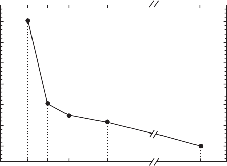
formation energies of defects increase as the size of the nanocrystal decreases, see Fig. 13.7 .
1.4 1.7 2.02 2.6 bulk
Nanocrystal diameter (nm)
0
0.25
0.5
0.75
1.5
1.25
1
Relative formation energy (eV)
Figure 13.7 Variation of the formation energy of a substitutional Mn impurity in a CdSe nanocrystal as a
function of the nanocrystal diameter. The increase in the formation energy is important to explain self-purifi cation in
nanocrystals [40] .
There are several experimental corroborations of this trend. The correlation of defect density
to the grain size was examined in nanocrystalline Pd and ZrO
2
upon irradiation with 4 MeV Kr
ions [42] . A drastic reduction of defect clusters in the small grains below 50 nm was found. In the
smallest ZrO
2
( 15 nm) and Pd grains ( 30 nm) no defects could be detected. PL experiments
performed on InAs QDs embedded in low-temperature (LT) grown GaAs led to the conclusion
that the PL quenching centres are located only in the GaAs barrier and not inside the QDs [43] .
In another work it was concluded from the structural characterization of self-organized InGaAs/
GaAs QDs grown on Si substrates that the dots themselves may be defect free [44] . However, only
relatively small dots can be defect free. So, e.g., when the InAs or InGaAs QDs exceeded certain
dimensions, dislocations were observed within the dots [45–47] .
CH013-I046325.indd 399CH013-I046325.indd 399 6/24/2008 3:45:29 PM6/24/2008 3:45:29 PM
400 Handbook of Self Assembled Semiconductor Nanostructures for Novel Devices in Photonics and Electronics
There also are many examples of experimentally found enhanced defect tolerance of the low-
dimensional structures. (It has to be noted that the role of native, technological and radiation-
induced defects on the performance of devices is the same.) The amphoterically doped GaAs or
single heterojunction GaAs/AlGaAs light-emitting diodes (LEDs) are much more sensitive to
proton-induced damage than the double heterojunction devices [48, 49] . Nanostructuring leads
to one order of magnitude enhancement of radiation hardness against high-energy heavy ion
bombardment in GaN layers [50] . The effect was tentatively explained as due to the increase
in the specifi c surface of the nanostructured sample which allows the migration of the defects
formed during the ion bombardment process towards the surface (see also [51] ), and due to the
enhanced dynamic annealing of these defects.
Furthermore, it was predicted theoretically that the high recombination rate of non-radiative
centres (lifetime killers) could be reduced by the low mobility of carriers and that (which is impor-
tant in the context of this chapter) the effect should be more pronounced in low-dimensional
structures [52] . Indeed, a strong reduction in the carrier diffusion length is observed going from
InGaAs QWs ( L
d
⬇ 2 . 7 μ m) to InAs QDs ( L
d
100 nm) [53] .
The increased tolerance of defects is one of the most important promises of the self-assembled
QD nanotechnology [54] . The basic argument is that more strongly localized carriers exhibit
reduced migration to non-radiative centres. The fi rst work on the defect tolerance of InAs QDs
has been reported in [55, 56] . The authors compared the PL of an array of self-assembled InAs/
GaAs QDs and of a single high-quality InGaAs QW. On GaAs substrates, the radiative quantum
effi ciency η was essentially the same for both structures. The growth on a commercial GaAs-on-
Si substrate with a high dislocation density entailed drastic quenching of the integrated PL inten-
sity and shortening of the carrier lifetime τ for the InGaAs QW, whereas both τ and η were not
modifi ed for the QD array. The authors came to the conclusion that the effi cient carrier capture
by InAs QDs, combined with the localized nature of QD excitons, hindered in this case the carrier
diffusion toward dislocations. Coexistence of growth-induced defect-related deep levels with InAs
QDs emitting bright luminescence was reported in [57] . InGaAs QD lasers grown on Si were suc-
cessfully fabricated [44, 431, 432] . Interestingly, a QD layer was utilized in [431] to suppress the
propagation of dislocations present in the GaAs buffer and to fabricate a low defect density active
QD region.
13.2.2 In(Ga)As/GaAs quantum dots
Irradiation with low- or medium-energy ions of In(Ga)As/GaAs QDs has been found to quench
the PL intensity at least one order of magnitude more slowly than in comparable QW structures
[58, 59] . The radiation hardness of the QD PL was observed also in experiments employing elec-
tron [60, 61] and proton [62–66, 81, 435] irradiation. An enhanced radiation resistance of the
electrical properties of the InGaAs/GaAs QD structures upon ion implantation [67] has been
shown, too.
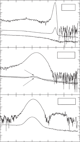
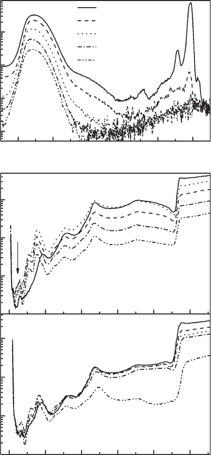
Let us consider in more detail the behaviour upon 2 MeV electron irradiation of three samples
containing one QD layer (sample 1 QD), fi ve QD layers (5 QD) and two coupled QWs (CQW)
[60] . The PL spectra of the as-grown samples taken at the measurement temperature T
m
1 0 K
upon excitation with an Ar
laser and their evolution versus electron irradiation fl uence are
shown in Fig. 13.8a–c . With increasing irradiation fl uence all samples exhibit a decrease in the
PL intensity. However, whereas in samples 1 QD and 5 QD the QD-related PL peaks could be
observed up to the fl uences Φ 1 1 0
17
and 2 1 0
17
c m
2
, respectively, the QW-related PL in
sample CQW was quenched already between Φ 2 1 0
16
and 5 1 0
16
c m
2
. This behaviour
is essentially the same at 10, 77 and 300 K. At electron fl uences Φ 1 1 0
17
c m
2
the PL of
bulk n-GaAs with a doping level of 1 1 0
17
c m
3
is completely suppressed [68] . Thus, Fig. 13.8
demonstrates a much higher tolerance of QDs with respect to the electron irradiation as com-
pared to bulk GaAs or QWs.
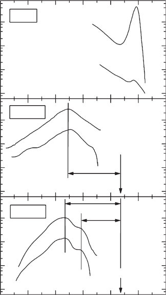
In order to separate the defect-related recombination processes in the GaAs barrier from those
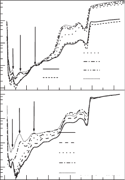
in the QDs and QWs themselves, the samples were investigated using resonant excitation by
means of a Ti
–sapphire laser. Selected spectra taken at 12 K are shown in Fig. 13.9 . The excita-
tion energy 1.318 eV lies below the PL peak of the WL centred at 1.35–1.36 eV. As in the case of
CH013-I046325.indd 400CH013-I046325.indd 400 6/24/2008 3:45:30 PM6/24/2008 3:45:30 PM
Radiation Effects in Quantum Dot Structures 401
the above-band gap excitation, the PL intensity degradation of the CQW sample is much stronger
than that of the QD samples. The behaviour observed upon 1 MeV proton irradiation [62] and
low-energy Ar ion bombardment [58] is completely analogous, as illustrated in Fig. 13.10 .
Possible processes leading to the quenching of the PL intensity upon electron irradiation are:
1. Capture and non-radiative recombination of photoexcited carriers at defects in the GaAs
barrier. This process should infl uence the QW and QD luminescence to one and the
same extent, provided a linear recombination regime (no saturation) is ensured. In fact,
under these conditions the PL intensity of the k th centre I
k
is given by the expression
I
k
∝ gN N
kk ii
i
σσ/( )
∑
, where g is the carrier generation rate, σ
i
is the capture cross-section
and N
i
is the concentration of the i th centre, and the summation is made over all
recombination channels. However, upon above-band gap excitation with the Ar
laser
very different PL quenching rates for QD and CQW samples which had similar PL inten-
sities prior to irradiation were observed. This means that (i) there is an additional
irradiation-induced “ QW- and QD-internal ” non-radiative recombination channel that has
a much larger cross-section in the QW than in the QDs and (ii) QDs can effi ciently capture
carriers directly from the barrier.
2. If the QDs are fed by carriers also through the WL, the defect-induced non-radiative
recombination in the WL should infl uence the quenching rate of the QD PL. Therefore, an
experiment with QD PL excitation below the WL band edge is essential. The QD PL quench-
ing observed upon subband gap excitation ( Figs. 13.9 and 13.10 (bottom)) confi rms very
well the existence of an internal defect-related recombination mechanism in the QDs and
the QW and its greater infl uence in the latter.
10
0
10
1
10
2
10
3
10
0
10
1
10
4
1.0 1.1 1.4 1.51.2 1.3
10
2
10
3
10
1
10
2
10
3
10
4
10
4
10
0
E (eV)
as grown
as grown
T
m
10 K
CQW
1 QD
5 QD
1E17 e/cm
2
2E17 e/cm
2
2E17 e/cm
2
2E16 e/cm
2
5E16 e/cm
2
as grown
(c)
(b)
(a)
PL intensity (a.u.)
Figure 13.8 FTIR PL spectra of samples 1 QD, CQW and 5 QD measured at 10 K upon excitation with
the 457.9 nm line of an Ar
laser. The electron irradiation fl uence Φ is indicated at the spectra. The PL intensity is
normalized to the excitation power. The latter did not exceed ⬃ 10
2
W/cm
2
for as-grown samples to avoid PL and
detector saturation. For irradiated samples with a low PL intensity, the excitation power was increased to maximize
the signal [60] .
CH013-I046325.indd 401CH013-I046325.indd 401 6/24/2008 3:45:30 PM6/24/2008 3:45:30 PM
402 Handbook of Self Assembled Semiconductor Nanostructures for Novel Devices in Photonics and Electronics
3. The internal irradiation-induced non-radiative recombination mentioned above may
occur at defects created inside the QW (WL) and QDs as well as at the interfaces QW (WL)/
GaAs barrier, QD/WL and QD/GaAs barrier. The delocalization of carriers in the QW (WL)
plane perpendicular to the growth direction makes them interact with a much greater
number of defects than in QDs [58] . Thus, a priori a higher radiation hardness of the QD
PL is expected. The role of inhomogeneous strain in defect trapping at interfaces with pos-
sible subsequent separation or annihilation is diffi cult to evaluate. It cannot be excluded
that the differing strain gradients infl uence the defect reactions in the QW and QD to a dif-
ferent extent.
4. Another mechanism of the “ internal ” defect-induced PL quenching proposed in [69] and
corroborated by detailed calculations in [70] is the carrier tunnelling out of the QW or
QDs to defects created in the GaAs barrier. In fact, QDs and QWs have a different sensitivity
to defects in the adjacent barrier regions. This is due to a differing degree of the wavefunc-
tion penetration into the barrier. So, e.g., In
0.13
Ga
0.87
As QWs start to ‘ ‘ feel ” a free surface
located at distances less than about 20 nm [71] . The PL intensity of InAs/GaAs QDs, how-
ever, only degrades for a cap thickness of 9 nm or smaller [72] .
10
2
10
1
10
1
10
0
10
1
10
1
10
0
10
0
10
2
10
1
10
2
10
1
1.10 1.401.351.25 1.301.15 1.20
E (eV)
CQW
h
exc
1.444 eV
5E16 e/cm
2
2E17 e/cm
2
2E16 e/cm
2
h
exc
1.318 eV
h
exc
1.318 eV
as grown
(b)
(c)
1 QD
5 QD
PL intensity (a.u.)
3LO
2LO
3LO
as grown
as grown
(a)
T
m
12 K
Figure 13.9 PL spectra of samples 1 QD, CQW and 5 QD measured at 12 K upon excitation with a Ti
–
sapphire laser. The PL intensity is normalized to the excitation power. With the excitation energy hv
exc
lying near
enough to the QD PL band, resonances within the latter at energies being a multiple of the LO-phonon energy can
be observed so that a subset of the QD ensemble defi ned by the ground-state transition energy is probed [74] . The
energies of the phonons involve range from 29.6 eV (InAs LO-phonon in the WL) to 37.6 meV (GaAs LO-phonon in
the strained barrier layers adjacent to the QDs) [60] .
CH013-I046325.indd 402CH013-I046325.indd 402 6/24/2008 3:45:30 PM6/24/2008 3:45:30 PM
Radiation Effects in Quantum Dot Structures 403
Further insights into the mechanism of the radiation damage of the QD heterostructures
were obtained by using the PL excitation (PLE) and time-resolved PL (TRPL) spectroscopy [61,
63–66, 73] . In samples A and B used in [65, 66] , the active layer together with GaAs clad-
ding layers were placed between two AlGaAs barriers, with a GaAs capping layer on top of the
whole structure. Sample A had an active layer composed by the QD layer, with a dot density of
⬇ (3–5) 1 0
10
c m
2
, overgrown by a 2 nm In
0.25
Ga
0.75
As QW. Sample B had a dot density of
⬇ 10
9
c m
2
in an active layer composed by a single QD layer. The irradiation by 2.4 MeV protons
with fl uences in the range from 1 1 0
12
to 1 1 0
14
c m
2
was performed at room temperature.
Usually the defects reduce the lifetime of non-equilibrium carriers and, consequently, their dif-
fusion length, thus limiting the carrier supply to the radiative recombination centres and killing
the PL intensity. However, because of the presence of the closely spaced AlGaAs barriers, the car-
rier capture by the QDs in the samples used in [65, 66] was not diffusion limited. That is why no
0
Ion dose (10
15
cm
2
)
12108246
QW
QW - 10 mW Ar
ⴙ
QW - 36 mW SPL
QDs - 36 mW SPL
QDs
QDs - 10 mW Ar
ⴙ
1.0
0.8
0.2
0.0
0.4
0.6
R (arb. units)
(b)
10
10
10
11
10
15
10
16
10
12
10
13
10
14
1
0.0001
0.1
0.01
0.001
1 MeV proton fluence/cm
2
Integrated QW PL
Integrated QD PL
Normalized PL signal
(a)
Figure 13.10 Top: PL intensity of a QD and a reference QW sample vs the 1 MeV proton fl uence upon above-band
gap excitation [62] . Bottom: Dependence of the PL intensity of a QD and a reference QW sample on the 300 eV
Ar ion fl uence. The measurements were done upon above-band gap (labelled 10 mW Ar
) or resonant excitation
(labelled 36 mW SPL) [58] .
CH013-I046325.indd 403CH013-I046325.indd 403 6/24/2008 3:45:30 PM6/24/2008 3:45:30 PM
404 Handbook of Self Assembled Semiconductor Nanostructures for Novel Devices in Photonics and Electronics
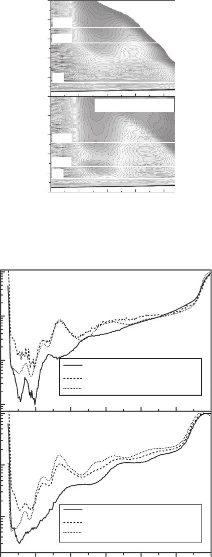
difference in the quenching factor of the PL intensity at a given irradiation dose was observed
at 7 K for the above-band gap and below-band gap excitation for all energies above the n 2
QD excited state ( Fig. 13.11b) . Thus, the loss of carriers occurs mainly in the dots themselves.
A probable reason of this effect is a tunnelling out of the dots to adjacent radiation-induced non-
radiative recombination centres. The situation changes dramatically, when the temperature
is increased to ⬃ 100 K ( Fig. 13.11c ). The PL intensity in the irradiated samples is recovered
(within ⬃ 10%) to the undamaged case. The channel leading to non-radiative recombination
is obviously not relevant at elevated temperatures. This observation was attributed to the
1.51.31.11.0
T 7 K
T 7 K
T 100 K
excited
state
excited
state
n 1
n 2
1.2 1.4
0
100 200 300
400
500
E (meV)
(c)
(b)
(a)
Intensity (arb. units)
as grown
1 10
13
protons/cm
2
2 10
13
protons/cm
2
5 10
13
protons/cm
2
1 10
14
protons/cm
2
WL/QW
GaAs
E
det
PL
Maximum
E
det
PL
Maximum
Intensity (arb. units)
LO
Energy (eV)
Figure 13.11 PL (a) and PLE (b, c) spectra of sample A with a dot density of ⬇ (3–5) 1 0
10
c m
2
for various
2.4 MeV proton irradiation doses, measured at 7 K (a, b) and 100 K (c) [65] .
CH013-I046325.indd 404CH013-I046325.indd 404 6/24/2008 3:45:31 PM6/24/2008 3:45:31 PM
Radiation Effects in Quantum Dot Structures 405
temperature-dependent competition of intradot relaxation and non-radiative recombination in the
fi rst excited state [74] . With increasing temperature intradot relaxation becomes more effi cient due
to the growth of the phonon density [75] . Consequently, the captured carriers reach the unper-
turbed ground state more quickly, thus overcoming the phonon bottleneck and bypassing tunnel-
ling. Upon further increasing the temperature above 100 K, the intensity decreases dramatically
with increasing dose [65] . This probably occurs because thermal activation into the barrier allows
the carriers to reach defect states in the latter without tunnelling. An important conclusion must
be drawn from this behaviour: the radiation hardness is temperature dependent.
Another striking feature of the PLE spectra is the increase upon irradiation of the PLE inten-
sity at energies corresponding to the low-lying QD excited states ( Fig. 13.11b and Fig. 13.12b ).
The effect is particularly well seen in Fig. 13.12b , where the PLE intensities for all doses have
been normalized to that of the as-grown sample at energies exceeding the GaAs band gap, and
in the contour plots ( Fig. 13.13 ). Qualitatively similar effects are observed when the temperature
is increased ( Fig. 13.12a ) or a reverse bias is applied to a diode structure with the dots located in
the space charge region ( Fig. 13.14 ) [65] . The radiation defects shift the Fermi level towards the
middle of the band gap, thus emptying the low-lying QD states from spectator carriers and per-
mitting the resonant absorption.
The results of the time-resolved PL (TRPL) measurements performed on sample A as a func-
tion of the irradiation dose, for resonant and non-resonant excitation, corroborate the PLE data.
No infl uence of the irradiation on the PL decay kinetics from the ground state is observed ( Fig.
13.15 ). However, the rise time shortens by about a factor of four for the dose 1 1 0
14
p/cm
2
,
both for the excitation into the barrier ( Fig. 13.15a ) and into the sublevels of the fi rst excited
state at 1.140 and 1.123 eV ( Fig. 13.15b and c ). This means that the rise time shortening
upon above-band gap excitation is caused by a carrier (exciton) loss in the QDs and not by any
reduction of the diffusion length in the barrier or the WL. As discussed above, the effect can be
explained by the tunnel escape of the carriers to adjacent defects. The ground state, having a
more localized wavefunction than the excited ones, remains essentially “ undamaged ” . Contrary
to measurements on electron irradiated QDs of another type [61] , no development of a second,
Sample B
n 2
n 1
100 200 300 400 500
n 2
n 1
LO
LO
WL
GaAs
GaAs
100 K
150 K
200 K
250 K
7 K
50 K
as grown
5 10
12
p/cm
2
1 10
13
p/cm
2
5 10
13
p/cm
2
2 10
13
p/cm
2
0
Intensity (a.u.)
(a)
(b)
ΔE (meV)
Figure 13.12 (a) PLE spectra vs the excess excitation energy Δ E E
exc
E
det
of the as-grown sample B with a
dot density of ⬇ 10
9
c m
2
taken at different temperatures. The spectra are normalized to the detection energy and to
the second excited state intensity. (b) PLE spectra of the same sample after irradiation with various 2.4 MeV proton
doses, recorded at the QD PL maximum at 7 K. The spectra are normalized to the intensity above the GaAs band gap
[66] .
CH013-I046325.indd 405CH013-I046325.indd 405 6/24/2008 3:45:31 PM6/24/2008 3:45:31 PM
150
100
50
250
100
50
0
200
150
250
200
n 2
LO
LO
n 1
n 2
n 3
Sample B
as grown
1.05 1.10 1.15 1.20 1.25
Detection energy (eV)
5 10
13
p/cm
2
E (meV)
Figure 13.13 Contour plots of the QD PL intensity as a function of the detection energy and the excess excitation
energy Δ E E
exc
E
det
for sample B at 7 K. The white lines denote PLE resonances from the excited states and
LO-phonons [66] .
n-doped sample
E
det
1.122 eV
n-doped sample
E
det
1.143 eV
n 1
excited states
P
as grown (0 V bias)
as grown (0 V bias)
as grown 1 V bias (empty QDs)
as grown 8 V bias (empty QDs)
1 10
14
protons/cm
2
1 10
14
protons/cm
2
(a)
(b)
T 7K
0
150
200 250
300100
50
ΔE (meV)
Normalized intensity (arb. units)
Figure 13.14 PLE spectra normalized to the wetting layer peak for as-grown and proton irradiated diode structures
with the dots located in the space charge region. (a) An n -doped sample and (b) a p -doped sample. The solid and dotted
lines show PLE spectra of charged and neutral QDs in the as-grown samples without and with bias, respectively. The
dashed lines show the PLE spectra of the QDs in the irradiated samples [65] .
CH013-I046325.indd 406CH013-I046325.indd 406 6/24/2008 3:45:32 PM6/24/2008 3:45:32 PM
Radiation Effects in Quantum Dot Structures 407
shorter decay time was observed. This difference was tentatively attributed to the heavier damage
caused by the electron doses up to 10
17
e/cm
2
used in [61] . Similarly, though a slight decrease of
the carrier lifetime was observed in irradiated QDs in [63, 64, 73] , it was much smaller than in
reference QW samples.
The above-mentioned facts bring up an important question. Do stable point defects created by
atomic displacements at room temperature (RT) exist inside the In(Ga)As QDs? In fact, their exist-
ence has never been proven. Since, as discussed in Section 13.1, the primary defects (vacancies
and interstitial atoms) are mobile at RT in GaAs and InAs, it is very likely that they are captured
at the interfaces (cf. [76] ). Moreover, the defects raise the free energy of the crystal, so that it is
only natural that the QDs expulse mobile defect components into the matrix. A related effect is
the “ self-purifi cation ” of nanocrystals [40] . The high radiation hardness of the ground state of
the QDs described above leads to the conclusion that the (small enough) QDs are defect free, at
least up to moderate irradiation fl uences. This, along with the localization of the wave function,
is a reason of the high radiation hardness of the QD structures.
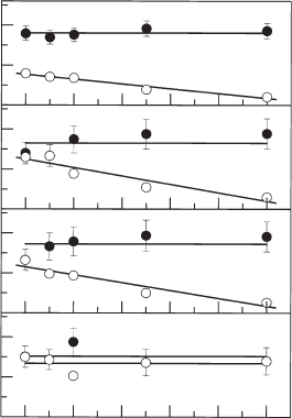
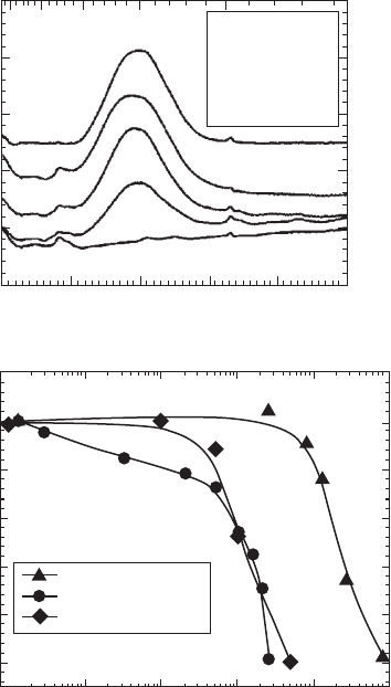
The behaviour upon 3 MeV proton irradiation and subsequent annealing of the optical absorb-
ance spectra of the intersubband transitions in In
0.3
Ga
0.7
As/GaAs QD samples and in GaAs/
AlGaAs and InGaAs/InAlAs multiple QW samples was investigated in [77] , see Fig. 13.16 . The
intensity of the intersubband transition was observed to decrease with increasing fl uence, and
the transition in QDs was completely depleted at a fl uence of 5 1 0
14
c m
2
. The comparison
of the radiation hardness of the QDs and the QWs could not be conclusive as the samples were
based on different materials systems. However, interesting differences in the annealing behaviour
were observed: whereas thermal annealing recovery of the depleted intersubband transitions was
observed in irradiated multiple QW samples, in the QD samples the transition was not recovered.
13.2.3 Other quantum dots
An enhanced tolerance of the PL to proton irradiation was also observed in the Ge/Si QDs [78] .
The underlying mechanisms should be similar to those in the InAs/GaAs QDs. However, the Ge
islands were very large (basis diameter ⬃ 200 nm), so that any effects of self-purifi cation or expul-
sion of defects out of the dots could not be expected.
1.0
0.5
0.0
1.0
0.5
0.0
0.5
1.0
0.0
0.5
0.0
1.0
0
6
8102
4
Dose (10
13
p/cm
2
)
Sample A
decay
(c)
(d)
(a)
(b)
E
exc
1.570 eV
E
exc
1.140 eV
E
exc
1.103 eV
E
exc
1.123 eV
rise
Time (ns)
Figure 13.15 Rise (open circles) and decay (solid circles) times from TRPL measurements of sample A. The detection
energy was at the ground state transition. (a) E
exc
1.570 eV (above the GaAs band gap); (b) E
exc
1.140 eV
(a sublevel of the 1st excited state); (c) E
exc
1.123 eV (another sublevel of the 1st excited state) [66] .
CH013-I046325.indd 407CH013-I046325.indd 407 6/24/2008 3:45:33 PM6/24/2008 3:45:33 PM
408 Handbook of Self Assembled Semiconductor Nanostructures for Novel Devices in Photonics and Electronics
There is, to the best of our knowledge, only one thorough report on the particle irradiation of
CdS
1
x
Se
x
QDs [79] (10 MeV electron irradiation was briefl y mentioned also in [80] ). The effect of
5 MeV and 10 MeV electron irradiation and subsequent annealing on the optical absorption of the
dots embedded in a borosilicate glass matrix was studied. Gradual smearing and vanishing of the
confi nement-related maxima and a considerable (up to 0.13 eV) blue shift of the absorption edge
were observed ( Fig. 13.17 ). Contrary to CdS
0.4
Se
0.6
, where the confi nement-related absorption
maxima vanished already after irradiation by 10
13
c m
2
( Fig. 13.17a ), in CdS
0.22
Se
0.78
QDs the
maxima, though smaller in intensity, were still visible even at 10
15
c m
2
( Fig. 13.17b ). Annealing
at 425–550 K resulted in the recovery of the initial absorption edge and the confi nement-
related maxima. The gradual smearing of the quantum size singularities was attributed to the
irradiation-induced ionization of the QDs due to electron (hole) transfer between the NCs and
irradiation-activated electron (hole) traps in the host matrix: with the increase of the irradiation
fl uence the transferred charge carriers occupy the confi nement-related levels in the dots, grad-
ually disabling the lower-energy transitions. The possibility of the creation of radiation defects
inside the QDs themselves was discussed [79] and found improbable: as the optical absorption
Figure 13.16 Top: Absorbance spectra of the intersubband transition in 3 MeV proton irradiated In
0.3
Ga
0.7
As/
GaAs QD samples. The spectra were obtained at RT after the samples were irradiated with different fl uences.
Bottom: Normalized integrated area of the intersubband transition as a function of irradiation fl uence obtained for
In
0.3
Ga
0.7
As/GaAs QD samples (diamonds), In
0.52
Ga
0.48
As/In
0.52
Al
0.48
As multiple QW samples (triangles) and
GaAs/Al
0.3
Ga
0.7
As multiple QW samples (circles) [77] .
600 800 1000 1200 1400 1600
Wave number (cm
1
)
1.2
0.4
0.2
0.6
0.8
1.0
16 14 812 10
(a) Unirradiated
(b) 1 10
13
cm
2
(c) 5 10
13
cm
2
(d) 1 10
14
cm
2
(e) 5 10
14
cm
2
(a)
(a)
(b)
(e)
(c)
(d)
Wavelength (μm)
Absorbance
InGaAS/InAIAs MQWs
InGaAS/GaAs MQDs
GaAs/AIGaAs MQWs
1.2
1.0
0.8
0.2
0.0
0.6
0.4
10
3
10
2
10
1
10
0
10
1
10
2
Dose (10
14
cm
2
)
Normalized integrated area
(b)
CH013-I046325.indd 408CH013-I046325.indd 408 6/24/2008 3:45:33 PM6/24/2008 3:45:33 PM