Henini M. Handbook of Self Assembled Semiconductor Nanostructures for Novel devices in Photonics and Electronics
Подождите немного. Документ загружается.

Advanced Growth Techniques of InAs-system Quantum Dots for Integrated Nanophotonic Circuits 549
large potential strain fi eld on the GaAs covered layer and creates a few nucleation sites. This con-
fi guration can be easily changed by varying the thickness of the covered layer and the amount of
InAs for the second layer QDs; in this way, the density of the second layer QDs can be controlled.
These results indicate that selective growth of InAs QDs can be achieved by using the In nano-
dots produced by the NJP method.
200 nm pitch (2.5 10
9
cm
2
)
In nano-dot
array
(NJP QDs)
4 μm
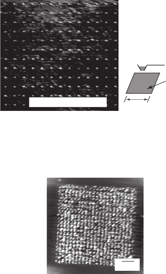
Figure 17.29 AFM image of a fabricated In nano-dot array.
1 μm
Figure 17.30 AFM image of the stacked high-density QD array.
17.3.4 Summary
We have demonstrated the use of a new nanoprobe-assisted technology that forms InAs QDs on
a GaAs substrate by a microfabrication technique (NJP) employing a specially designed canti-
lever. Using the NJP, uniform In nano-dot arrays were formed in a reproducible manner on an
MBE-grown surface by applying electric pulses between the tip and the sample. These In nano-
dot arrays were converted directly into InAs QD arrays by subsequent annealing with irradiation
of arsenic fl ux. Furthermore, we have demonstrated the selective area growth of high-density
InAs QDs by using site-controlled InAs QDs that were formed in the desired regions as templates.
The NJP method enables the formation of the required number of InAs QDs in a desired region. In
other words, the NJP method offers perfect selectivity in forming InAs QDs. An example of the inte-
gration of QDs into photonic devices is a photonic crystal-based ultra-fast all-optical switch which
CH017-I046325.indd 549CH017-I046325.indd 549 6/25/2008 3:17:33 PM6/25/2008 3:17:33 PM
550 Handbook of Self Assembled Semiconductor Nanostructures for Novel Devices in Photonics and Electronics
we are currently developing [5] . These devices use QDs as a non-linear optical material to switch the
optical signal pulses. For these devices, QDs should be formed only in the photonic crystal straight
waveguide area. The NJP method will enable the formation of the required number of QDs in a
desired region with both high uniformity and high density. Furthermore, we can achieve the required
volume of QDs for optical switching by combining this site-controlled QD formation technique with
the subsequent stacking of spatially ordered InAs QD arrays using MBE growth [31] . In addition
to our proposed PC-based devices [5] , the NJP method has applications to other optical switching
devices, including future high-performance functional devices such as regular arrays of quantum
bits and single-photon emitters for quantum computers and quantum communications [10, 11] .
References
1. Y. Arakawa and H. Sakaki , Multidimensional quantum well laser and temperature dependence of
its threshold current , Appl. Phys. Lett. 40 , 939 – 941 ( 1982 ) .
2. M. Sugawara , N. Hatori , T. Akiyama , Y. Nakata , and G. Ishikawa , Quantum-dot semiconductor
optical amplifi ers for high bit-rate signal processing over 40 Gbit/s , Jpn. J. Appl. Phys. 40 , L488 –
L491 ( 2001 ) .
3. S. Kohmoto , H. Nakamura , T. Ishikawa , and K. Asakawa , Site-controlled self-organization of indi-
vidual InAs quantum dots by scanning tunneling probe-assisted nano-lithograph , Appl. Phys.
Lett. 75 , 3488 – 3490 ( 1999 ) .
4. S. Ohkouchi , Y. Nakamura , H. Nakamura , and K. Asakawa , InAs nano-dot array formation using
nano-jet probe for photonics applications , Jpn. J. Appl. Phys. 44 , 5777 – 5780 ( 2005 ) .
5. K. Asakawa , Y. Sugimoto , Y. Watanabe , N. Ozaki , A. Mizutani , Y. Takata , Y. Kitagawa , H. Ishikawa ,
N. Ikeda , K. Awazu , X. Wang , A. Watanabe , S. Nakamura , S. Ohkouchi , K. Inoue , M. Kristensen ,
O. Sigmund , P.I. Borel , and R. Baets , Photonic crystal and quantum dot technologies for all-optical
switch and logic device , New J. Phys. 8 , 208 ( 2006 ) .
6. K. Tajima , All-optical switch with switch-off time unrestricted by carrier lifetime , Jpn. J. Appl.
Phys. 32 , L1746 – L1749 ( 1993 ) .
7. H. Nakamura , Y. Sugimoto , K. Kanamoto , N. Ikeda , Y. Tanaka , Y. Nakamura , S. Ohkouchi ,
Y. Watanabe , K. Inoue , H. Ishikawa , and K. Asakawa , Ultra-fast photonic crystal/quantum dot
all-optical switch for future photonic network, Opt. Express 12 , 6606 – 6614 ( 2004 ) .
8. N. Ozaki , Y. Takata , S. Ohkouchi , Y. Sugimoto , Y. Nakamura , N. Ikeda , and K. Asakawa , Selective
area growth of InAs quantum dots with a metal mask towards optical integrated circuit devices ,
J. Cryst. Growth 301 –302 , 771 – 775 ( 2007 ) .
9. T. Yoshie , A. Scherer , J. Hendrickson , G. Khitrova , H.M. Gibbs , G. Rupper , C. Ell , O.B. Schchekin ,
and D.G. Deppe , Vacuum Rabi splitting with a single quantum dot in a photonic crystal nanocav-
i t y , Nature 432 , 200 – 203 ( 2004 ) .
10. E. Waks , K. Inoue , C. Santori , D. Fattal , J. Vuckovic , G.S. Solomon , and Y. Yamamoto , Secure com-
munication: quantum cryptography with a photon turnstile , Nature 420 , 762 ( 2002 ) .
11. A. Imamoglu , D.D. Awschalom , G. Burkard , D.P. DiVincenzo , D. Loss , M. Sherwin , and A. Small ,
Quantum information processing using quantum dot spins and cavity QED , Phys. Rev. Lett. 83 ,
4204 – 4207 ( 1999 ) .
12. S. Ohkouchi , Y. Nakamura , H. Nakamura , and K. Asakawa , Indium nano-dot arrays formed by
fi eld-induced deposition with a nano-jet probe for site-controlled InAs/GaAs quantum dots , Thin
Solid Films 464– 465 , 233 – 236 ( 2004 ) .
13. Y. Nakamura , N. Ikeda , S. Ohkouchi , Y. Sugimoto , H. Nakamura , and K. Asakawa , Regular array
of InGaAs quantum dots with 100-nm-periodicity formed on patterned GaAs substrates , Physica
E 21 , 551 – 554 ( 2004 ) .
14. Y. Nakamura , N. Ikeda , S. Ohkouchi , Y. Sugimoto , H. Nakamura , and K. Asakawa , Two-dimensional
InGaAs quantum-dot arrays with periods of 70–100 nm on artifi cially prepared nanoholes , Jpn.
J. Appl. Phys. 43 , L362 – L364 ( 2004 ) .
15. K. Nishi , H. Saito , S. Sugou , and J.S. Lee , A narrow photoluminescence linewidth of 21 meV
at 1.35 μ m from strain-reduced InAs quantum dots covered by In
0.2
Ga
0.8
As grown on GaAs
substrates, Appl. Phys. Lett. 74 , 1111 – 1113 ( 1999 ) .
CH017-I046325.indd 550CH017-I046325.indd 550 6/25/2008 3:17:34 PM6/25/2008 3:17:34 PM
Advanced Growth Techniques of InAs-system Quantum Dots for Integrated Nanophotonic Circuits 551
16. S. Ohkouchi , Y. Nakamura , H. Nakamura , N. Ikeda , Y. Sugimoto , and K. Asakawa , Selective
growth of high quality InAs quantum dots in narrow regions using in situ mask , J. Cryst. Growth
293 , 57 – 61 ( 2006 ) .
17. Y. Sugimoto , N. Ikeda , N. Carlsson , K. Asakawa , N. Kawai , and K. Inoue , Fabrication and charac-
terization of different types of two-dimensional AlGaAs photonic crystal slabs , J. Appl. Phys. 91 ,
922 – 929 ( 2002 ) .
18. N. Ikeda, H. Kawashima, Y. Sugimoto, T. Hasama, K. Asakawa, and H. Ishikawa, Coupling char-
acteristic of micro planar lens for 2D photonic crystal waveguides, 19th International Conference
on InP and related materials (IPRM) (2007).
19. N. Ozaki , Y. Kitagawa , Y. Takata , N. Ikeda , Y. Watanabe , A. Mizutani , Y. Sugimoto , and
K. Asakawa , High transmission recovery of slow light in a photonic crystal waveguide using a
hetero group-velocity waveguide , Opt. Exp. 15 , 7974 – 7983 ( 2007 ) .
20. C. Lee and A.L. Barabasi , Spatial ordering of islands grown on patterned surfaces , Appl. Phys. Lett.
73 , 2651 – 2653 ( 1998 ) .
21. S. Ohkouchi , Y. Nakamura , H. Nakamura , and K. Asakawa , Nano-probe-assisted technology of
indium-nano-dot formation for site-controlled InAs/GaAs quantum dots , Physica E 21 , 597 – 600
( 2004 ) .
22. S. Ohkouchi , Y. Sugimoto , N. Ozaki , H. Ishikawa , and K. Asakawa , Selective growth of InAs quan-
tum dots using In nano-dot arrays formed by nano-jet probe method , J. Cryst. Growth 301 –302 ,
726 – 730 ( 2007 ) .
23. H.J. Mamin , P.H. Guethner , and D. Ruger , Atomic emission from a gold scanning-tunneling-micro-
scope tip , Phys. Rev. Lett. 65 , 2418 – 2421 ( 1990 ) .
24. N. Aoki , K. Fukuhara , T. Kikutani , A. Oki , H. Hori , and S. Yamada , Fabrication of buried metal dot
structure in split-gate wire by scanning tunneling microscope , Jpn. J. Appl. Phys. 35 , 3738 – 3742
( 1996 ) .
25. K. Higa and T. Asano , Joule heating of fi eld emitter tip fabricated on glass substrate , Jpn. J. Appl.
Phys. 43 , 2749 – 2750 ( 2004 ) .
26. G. Taylor , Electrically driven jets , Proc. Roy. Soc. Lond. A 313 , 453 – 475 ( 1969 ) .
27. R.P.A. Hartman , D.J. Brunner , D.M.A. Camelot , J.C.M. Marijnissen , and B. Scarlett ,
Electrohydrodynamic atomization in the cone-jet mode physical modeling of the liquid cone and
jet , J. Aerosol Sci. 30 , 823 – 849 ( 1999 ) .
28. T. Chikyow and N. Koguchi , MBE growth method for pyramid-shaped GaAs micro crystals on
ZnSe(001) surface using Ga droplets , Jpn. J. Appl. Phys. 29 , L2093 – L2095 ( 1990 ) .
29. R.S. Wagner and W.C. Ellis , Vapor-liquid-solid mechanism of single crystal growth , Appl. Phys.
Lett. 4 , 89 – 90 ( 1964 ) .
30. N. Koguchi , K. Ishige , and S. Takahashi , New selective molecular-beam epitaxial growth method
for direct formation of GaAs quantum dots , J. Vac. Sci & Technol. B
11 , 787 – 790 ( 1993 ) .
31. Y. Nakamura , N. Ikeda , S. Ohkouchi , Y. Sugimoto , H. Nakamura , and K. Asakawa , Two-
dimensional InGaAs quantum-dot arrays with periods of 70–100 nm on artifi cially prepared
nanoholes , Jpn. J. Appl. Phys. 43 , L362 – L364 ( 2004 ) .
CH017-I046325.indd 551CH017-I046325.indd 551 6/25/2008 3:17:35 PM6/25/2008 3:17:35 PM

Nanostructured Solar Cells
S.G. Bailey ,
1
Seth Hubbard,
2
and R.P. Raffaelle
2
1
Space Environment and Experiments Branch, NASA Glenn Research Center,
MS 302-1, Cleveland, OH 44135;
2
Rochester Institute of Technology, Rochester, NY 14623
18.1 Introduction
There has been considerable investigation regarding the potential for the use of nanomateri-
als and nanostructures to increase the effi ciency of photovoltaic devices [1] . Examples of such
investigation include the use of materials and/or combinations of materials that provide either
one-dimensional, two-dimensional, or even three-dimensional quantum confi nement (i.e. quan-
tum wells [2] ; quantum wires [3] ; or quantum dots [4,5] , respectively). Quantum confi nement
refers to the fact that a dimension or dimensions associated with a given material are smaller
than the Bohr exciton radius for that material. This results in the possible electronic states asso-
ciated within the material to deviate from the ordinary band theory of solids and begin to show
discrete-like optoelectronic behaviour more familiar with atoms or molecules. The term nano-
material would generally be reserved for isolated materials that have at least some degree of
quantum confi nement (e.g. colloidal suspensions of semiconducting nanocrystals, fullerenes,
single- or multi-wall carbon nanotubes). A nanostructure would commonly refer to a composite
material in which the boundaries of one material by another results in the dimensions of the fi rst
material to be on the nanoscale. A prime example of this would be an extremely thin (i.e. a few
nanometres) epitaxially grown layer of a narrow band semiconductor within a wider band gap
host material. This resulting “ nanostructured ” material would be a quantum well if the thick-
ness of this narrow band gap layer is of a suffi ciently small dimension, as mentioned above.
Nanostructures can also be comprised of arrays of individual nanomaterials. Semiconducting
quantum dots (QDs) can be combined in a three-dimensional array, often through the use of self-
ordering. The discrete-like energy levels of the quantum dots will combine and form bands of
allowed energy states in an analogous way in which atomic energy levels combine to produce the
energy bands in conventional solids. In this case, it is easy to see why quantum dots are some-
times referred to as “ super atoms ” . By changing the quantum dot size and the spacing between
the quantum dots, the optoelectronic bandstructure will change in ways similar to the way a
semiconductor bandstructure changes with compositional doping. The shift in the effective band
gap will vary inversely with the particle size of the dot [6] .
Quantum wells or quantum wires can also be arrayed. The use of many closely spaced quan-
tum wells, or a multiple quantum well, is a very well-known structure within the optoelectronic
industry. This has been a prime means of “ band gap engineering ” semiconducting materials. By
changing the quantum well width, spacing of the wells (i.e. the thickness of the barriers between
the wells), and the composition well and/or barrier material, one can effectively “ tune ” the band
gap to values that cannot be achieved using merely compositional changes alone.
CHAPTER 18
CH018-I046325.indd 552CH018-I046325.indd 552 6/27/2008 5:20:08 PM6/27/2008 5:20:08 PM
Nanostructured Solar Cells 553
The role of a nanomaterial or nanostructure in a given photovoltaic solar cell design can vary
dramatically. In some cases, the goal may be simply to provide the means to disassociate exci-
tons throughout a bulk material as in the use of colloidal quantum dots in organic or polymeric
solar cells. In other cases, the use of a nanostructure is motivated by the desire to band gap engi-
neer a device in a similar approach to what is done more conventionally through compositional
changes in a device, albeit in regimes where compositional solutions may not be readily available.
A more ambitious use of nanostructures for photovoltaics lies in the desire to exploit underlying
quantum confi nement concepts to fundamentally change the way we can exploit photoconver-
sion for electrical energy production. Examples of quantum mechanical phenomena offered by
nanostructures that could be exploited to exceed the standard Shockley–Quiesser limit for a con-
ventional solar cell [7] (i.e. the maximum thermodynamic effi ciency for the conversion by a sin-
gle band gap cell of unconcentrated solar irradiance into electrical free energy of approximately
31%) are hot carrier effects, multiple exciton generation, phonon bottlenecking, and up- and
down-conversion. Hot-carrier solar cells [8] attempt to use nanostructures to obviate the normal
thermalization processes associated with conventional solar cells, or in other words, extract the
carriers before they relax down to the conduction band edge of the host semiconductor. Solar
cells attempting to exploit the multiple exciton generation processes demonstrated by colloidal
by quantum dots hope to produce multiple electron–hole pairs per photon through this inverse
Auger impact ionization [9] . Finally, the use of quantum dot arrays may allow approaches that
expand the spectral response of conventional solar cells by shifting incoming photon energy from
inaccessible regions or regions of the spectrum that are ineffi ciently converted to more favoura-
ble energy ranges, and potentially provide the means for multiband intermediate band cells [10] .
This chapter discusses a few of the recent approaches to produce nanostructured solar cells.
18.2 Quantum dot solar cells
The term quantum dot solar cells is somewhat ambiguous as it is colloquially used to refer to two
general types of solar cells in which both the role of the quantum dots, the materials and synthe-
sis methods used to create them, and the types of cells in which they are used, are drastically dif-
ferent. These two classes of cells are those which use colloidal quantum dots in a polymer matrix
and their crystalline counterparts which utilize epitaxially grown, normally Stranski–Krastanov
(SK) mode, quantum dots (QDs). The motivation for the former class is due to the rapid increase
in device effi ciencies in polymer solar cells with the addition of nanomaterials, such as CdSe
quantum dots and more recently fullerenes. This work has led to the type of solar cell called a
distributed heterojunction solar cell. The latter class of quantum dot solar cells are those involv-
ing the epitaxially grown quantum dots, usually comprised of III–V materials in the form of
quantum dot arrays (QDAs). Much of the motivation for the research in this area was provided
by the theoretical work on intermediate band solar cells (IBSCs). It has been proposed that an
IBSC could be achieved via a quantum dot array embedded into a suitable host solar cell struc-
ture. It is still somewhat of an open debate whether or not the IBSC band solar cell as proposed in
the aforementioned theoretical treatments is theoretically achievable using a QDA.
18.2.1 Intermediated band solar cells
Theoretical results of Luque and Marti have shown that a photovoltaic device with a single inter-
mediate band of states resulting from the introduction of quantum dots offers a potential effi -
ciency of 63.2% [11] . This was extended to two intermediate bands and a limiting effi ciency of
71.7% was calculated [9] . The enhanced effi ciency results from converting photons of energy
less than the band gap of the cell by an intermediate band. The intermediate band provides a
mechanism for low-energy photons to excite carriers across the energy gap by a two-photon
process. In principle, the use of a QDA to achieve this intermediate band may have some distinct
advantages to that of a multiple quantum well (MQW), such as in directionality of the illumina-
tion that can result in the ability to optically excite carriers from the intermediate band into the
CH018-I046325.indd 553CH018-I046325.indd 553 6/27/2008 5:20:09 PM6/27/2008 5:20:09 PM

554 Handbook of Self Assembled Semiconductor Nanostructures for Novel Devices in Photonics and Electronics
host semiconductor conduction band and in terms of the practical range of tunability offered by
a QDA over that of an MQW.
Quantum dots offer the potential to control the intermediate band energies since the indi-
vidual quantum energy levels associated with isolated quantum dots is a function of their size,
separation from one another, and material composition. Placing the appropriate quantum dot
material of the necessary size into an organized matrix within an ordinary p-i-n structure solar
cell should result in the formation of accessible energy levels within what would normally be the
forbidden band of the device. A simple schematic of one such proposed intermediate band solar
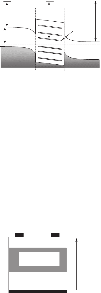
cell structure is shown in Fig. 18.1 .
Grid fineer
p-InGaP window
p-GaAs emitter
Back contact
n-InGaP window
n⬘-GaAs buffer
n⬘-GaAs substrate
n⬘-GaAs base
InAs QDA InGaAs
Figure 18.1 Intermediate band cell structure.
The electronic wavefunctions associated with the discrete electronic states of the individual
quantum dots in the QDA array will overlap creating “ mini-bands ” in the host semiconductors ’
band gap. The composition and related properties (i.e. bulk band gap, electron affi nity, effective
masses, etc.), size, symmetry, and spacing of the quantum dots need to be chosen to produce
mini-bands which are appropriately spaced within the band gap of the host material (see Fig.
18.2 ). The majority of the work to date on this type of QDA for use in a solar cell has been on the
development of InAs QDAs in GaAs. Fortunately, the strain associated with the SK growth of QDs
acts to self-align the QD into vertical columns to produce the desired arrays as each additional
layer is added in this system. More recently, it has been proposed that QDAs of Si could be used in
a similar fashion in an amorphous silicon solar cell [12] .
A major challenge in designing solar cells which can take maximum advantage of a QDA is the
balance between balancing absorption and transport. A QDA with many layers could improve the
subhost band gap absorption at the cost of the effi cient extraction photo-generated carriers from
the quantum-confi ned region [13] due to the diminished electric fi eld across the QDA within the
intrinsic region of the device and increased probability of recombination and radiative losses.
Transport of carriers generated in bulk would presumably also suffer as the QDA is widened. On
the other hand, a QDA that is too thin would provide little benefi t from photoconversion of the
subhost band gap illumination to offset the increased defect density that would be likely to result
from its inclusion. Recent modeling of an IBSC based on quantum dot supracrystals was under-
taken to engineer optimum array dimensions necessary for maximum solar cell effi ciency [14] .
CH018-I046325.indd 554CH018-I046325.indd 554 6/27/2008 5:20:09 PM6/27/2008 5:20:09 PM
Nanostructured Solar Cells 555
Using the material system of an InAsN/GaAsSb quantum dot supralattice, it was shown that
the power conversion effi ciency of the IBSC was maximized by a quantum dot size of approxi-
mately 4.7 nm. It was noted that solar cells based on these quantum dots may also show
enhanced radiation hardness [15] and improved collection effi ciency [16, 17] .
Transport through the QDA can be enhanced by reducing the spacing between the QD layers.
This, of course, will change the absorption spectrum and reduce the 3D quantum confi nement.
Taken to the extreme, this type of a cell would approach what would be in a sense a quantum
wire solar cell. The closely spaced QDs would form nanoscale wires across the intrinsic region of
the device (see Fig. 18.3 ) . In such a device, the presence of a one-dimensional electron gas across
the junction region will result in a fast collection of the carriers photo-generated in the quantum
wires region, and the solar cell output will thus fully benefi t from improved absorption properties
associated with the presence of quantum confi ned states. In practice, arrays of vertical quantum
wires can be formed by a self-organization process occurring during the deposition of ultra-short
period stacks of highly strained/strain balanced fi lms of III–V semiconductors (e.g InAs/AlAs on
InP, InGaAs/InGaP on GaAs, etc.). One could also envision potentially producing solar cells with
such structures utilizing other materials through electron lithography (wire widths in excess of
20–30 nm).
E
cp
E
vp
p-type
region
Insulating
region
n-type
region
Quantum dot
mini-bands
E
g
χ
QD
χ
P
χ
n
Vac
Figure 18.2 Idealized energy band diagram of an intermediate band solar cell.
p
⫹
-emitter
n-Base
i-region
(Quantum wires)
Z(001)
Figure 18.3 Schematic representation of the proposed vertical quantum wire device.
Modeling of a quantum wire structure was undertaken in which the dots were assumed to
stack vertically in the cell [18] . For an indium phosphide emitter and base with indium arsi-
nide wires, there was a peak effi ciency with quantum wire length. It has been suggested that the
quantum wire solar cell, while circumventing carrier collection issues (when compared to quan-
tum dot and quantum well systems), may also provide a signifi cantly larger density of states and
consequently enhanced photo-absorption.
CH018-I046325.indd 555CH018-I046325.indd 555 6/27/2008 5:20:10 PM6/27/2008 5:20:10 PM
556 Handbook of Self Assembled Semiconductor Nanostructures for Novel Devices in Photonics and Electronics
18.3 Quantum dot growth
18.3.1 Stranksi–Kranstanow quantum dots
The ideal QD behaves much like the idealized box in the famous quantum mechanical of the par-
ticle-in-a-box problem. This QD is a structure capable of confi ning carriers (electrons and holes)
in three-dimensions, allowing zero dimensions (0D) in their degrees of freedom, and creating
atom-like levels with discrete (Dirac delta) densities of states. This is why quantum dots can also
be visualized and described as “ artifi cial atoms ” . In SK grown QDs, this structure is achieved by
having a very small volume of a low band gap material embedded in larger band gap material(s),
thus creating the potential barrier for quantum confi nement of the carriers. Until recently, such
three-dimensional confi nement in semiconductor structures existed mostly in theoretical treat-
ments. In addition to SK growth, other approaches to manufacture quantum dots made use of
photolithography and etching. While providing good control of the order and offering design
fl exibility; these types of processing affected the interfaces, introducing impurities and surface
damage that limited the optical performance of these quantum structures.
The SK growth mode for III–V QDs takes advantage of a strain-induced transformation that
happens naturally in the initial stages of growth for lattice-mismatched materials. The growth
usually starts layer by layer, and after a certain critical thickness is reached, the structure spon-
taneously forms nanometre-size islands (SK mode [19] ) that show good size uniformity and large
surface densities. In this process, the growth is interrupted [20] immediately after formation
of the islands, but before the islands reach a size for which strain relaxation and misfi t disloca-
tions occur. This spontaneous island formation during growth precludes the interface quality
problems often associated with ex situ processed quantum structures of low dimensionality.
The mechanisms of SK strain-induced QD growth in molecular beam epitaxy (MBE) are fairly
straightforward. However, in the case of organometallic vapour phase epitaxy (OMVPE) to initi-
ate the SK growth mode, growth temperatures must be reduced to well below the values typically
associated with mass-transport limits [21] . The result is that QD nucleation, growth, and uni-
formity becomes much more sensitive to OMVPE growth parameters, such as growth tempera-
ture, growth rate and V/III ratio. However, for commercial production of solar cells, the OMVPE
has defi nite advantages in terms of production rate, scalability, and cost to its MBE counterpart.
The growth of SK mode InAs QDs on GaAs by organometallic vapour phase epitaxy (OMVPE)
or metal organic chemical vapour deposition (MOCVD) commonly use metallorganics, such
as trimethyl gallim (TMGa) and trimethyl indium (TMIn) as precursor materials, along with
hydrides phosphine (PH
3
), arsine (AsH
3
), and 1% AsH
3
in hydrogen. The typical growth tem-
peratures are between 500 and 700
o
C and a pressure of around 600 torr. An example of how
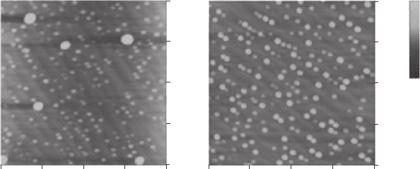
OMVPE growth conditions effect InAs quantum dots on GaAs can be seen in Fig. 18.4 .
0
(a) (b)
0.25 0.50 0.75 1.00
μm μm
0
0
0.25
0.25
0.15 nm
0.0 nm
0.30 nm
0.50
0.50
0.75
0.75
1.00
1.00
0
0.25
0.50
0.75
1.00
Figure 18.4 AFM micrographs near wafer center for OMVPE-grown SK mode InAs QDs grown on GaAs with
V–III ratios of (a) 58 and (b) 12 [20] .
CH018-I046325.indd 556CH018-I046325.indd 556 6/27/2008 5:20:11 PM6/27/2008 5:20:11 PM
Nanostructured Solar Cells 557
20 nm
10
0.1
1
10
100
1000
10000
15.0
Omega - two theta (deg)
Count rate (a.u.)
GaN
InN
500
400
300
100 nm
200
20 nm
10
20 nm
10
20 nm
10
15.5
16.0
16.5 17.0 17.5 18.0
Figure 18.5 AFM image of InN quantum dots grown on a GaN buffer layer. The presence of InN material has been
verifi ed by X-ray diffraction spectrum shown on the inset [21].
75 sec
400 sec
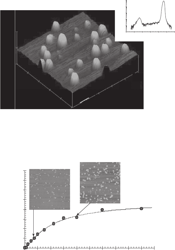
Figure 18.6 Height of the InN islands as a function of growth time for a series of samples deposited at a
temperature set point of 720 °C. Insets show the AFM image from 5 mm ⫻ 5 mm scans of samples grown for 75
seconds and 400 seconds. The lines through the data points are provided as a guide to the eye [21].
There are other examples of quantum dot formation by OMVPE. A recent study of InN dots syn-
thesized on GaN templates has been reported [22] . Using sapphire substrates, a 1.5 micron thick
GaN template was grown using a standard two-step process prior to the deposition of InN. The lat-
tice mismatch between InN and GaN is quite large ( ⬎ 10%), causing to proceed in a three-dimen-
sional mode. Indeed, AFM images revealed the formation of discrete InN islands on the GaN surface,
as illustrated in Fig. 18.5 and similar to reports from other groups [23, 24] . X-ray diffraction meas-
urements confi rmed the deposition of InN in the sample set grown on GaN templates (see Fig. 18.5
inset). The strong peak near 17.3 ° seen in the Fig. 18.5 inset corresponds to diffraction from the
GaN lattice in the buffer layer, while the weaker peak near 15.8 ° is in the range expected for epitax-
ial InN. The intensity of the InN-related peak generally increases with growth time, and both the
position and full width-at-half maximum exhibit a slight dependence on the growth conditions.
Figure 18.6 demonstrates the evolution in the height of the InN islands with the growth
time under fi xed deposition conditions. The InN islands do not form until approximately 15 to
20 seconds of growth time, and they are still discrete after 900 seconds of growth. The delayed
CH018-I046325.indd 557CH018-I046325.indd 557 6/27/2008 5:20:12 PM6/27/2008 5:20:12 PM
558 Handbook of Self Assembled Semiconductor Nanostructures for Novel Devices in Photonics and Electronics
onset of three-dimensional islands is consistent with a Stranski–Krastanov growth mode for the
deposition of InN on a GaN template. The height of the InN islands increases rapidly from 7 nm
to 50 nm as the growth time increases from 25 to 225 seconds, and then begins to saturate,
approaching 80 nm as the growth time increases further from 300 to 900 seconds. At fi rst, the
density of the InN islands remains constant near 5 ⫻ 1 0
8
cm
⫺ 2
, and the distribution of island
sizes is relatively narrow, as illustrated by the AFM image of the sample grown for 75 seconds
(see inset in Fig. 18.5) . However, a second group of much smaller islands appears in structures
with a growth time of 300 seconds or greater, resulting in a total InN island density approaching
1 ⫻ 1 0
9
cm
⫺ 2
. The bimodal distribution of InN islands is evident in the AFM image of the 400
second sample also seen in the inset in Fig. 18.5 . The appearance of the second group of InN
islands near 300 seconds in growth time corresponds to the saturation in the height of the initial
set of InN islands.
Photoluminescence emissions from both dots and wetting layer are observed in other lattice-
mismatched III–V material systems, most notably InAs on GaAs [25] . Non-radiative recom-
bination at surface states is well known to degrade the photoluminescence of many III–V
semiconductors, and most PL studies of InAs dots and wetting layers on GaAs employ capped
structure and/or low-temperature measurements to enhance emission intensities. However,
nitride materials can behave quite differently. For example, room temperature photoluminescence
emission is observed in thin, uncapped GaN fi lms grown on wider energy gap AlGaN layers [26] .
While surface states may be less severe in nitride materials, it has been observed that the buffer
layer quality has a strong impact on the intensity of PL emissions from InN dots.
Quantum dots of Si have also been formed by alternating layers of silicon dioxide followed by
a silicon-rich layer of the same material and then heat treating [27] . On heating, the surface
energy minimization favoured the precipitation of silicon into spherical quantum dots. These
quantum dots could be inserted into an amorphous silicon solar cell. A proposed all-silicon tan-
dem cell has been proposed.
18.4 Organic quantum dot solar cells
Improvement in polymer solar cell performance has long suffered from several shortcomings (i.e.
low electron mobility, absorption characteristics that were not well suited to the solar spectrum,
environmental degradation, etc.). However, the lure of potential low cost and large area manu-
facturing of thin fi lm fl exible solar cells continued to attract researchers [28] . A main fundamen-
tal limitation associated with the use of organic thin fi lms for PV is that photonic absorption in
these materials produces bound state excitons. Dissociation of these charge pairs requires a sub-
stantial potential difference across a polymer–metal or polymer–semiconductor junction, pro-
vided the excitons are near the interface. Thus, polymer solar effi ciencies improved dramatically
with the introduction of the use of nanomaterial/conjugated polymer complexes or what are
now commonly referred to as bulk heterojunction solar cells [29] . This refers to the fact that the
materials that are responsible for both the donors and acceptors are intimately mixed through-
out the absorber layer of the device.
A suitable choice of QD, or alternatively a fullerene, can provide the necessary electron-accept-
ing impurity in a polymer matrix. Thus, under illumination a preferential transfer of electrons
from the excitons to the acceptors leaves behind holes. This process is known as photo-induced
charge transfer. The carriers, once liberated from one another, are now free to be transported
through the conjugated polymer. All that remains is to incorporate these composites or blends
into a suitable device structure.
A variety of acceptor materials have been introduced into conjugated polymers to produce
photovoltaic devices (i.e. buckminster fullerenes [30] , CdSe quantum dots, CdSe nano rods [31] ,
and single-wall carbon nanotubes [32] (SWCNT)) [33] . The devices are produced by placing the
doped polymeric fi lms between a transparent conductive oxide, typically indium tin oxide (ITO),
top contact and a metallic back contact. There has also been recent work on thin fi lm polymeric
solar cells which incorporate quantum dots as well as quantum dot/SWCNT complexes [34] .
CH018-I046325.indd 558CH018-I046325.indd 558 6/27/2008 5:20:14 PM6/27/2008 5:20:14 PM