Henini M. Handbook of Self Assembled Semiconductor Nanostructures for Novel devices in Photonics and Electronics
Подождите немного. Документ загружается.


Advanced Growth Techniques of InAs-system Quantum Dots for
Integrated Nanophotonic Circuits
Kiyoshi Asakawa ,
1
Nobuhiko Ozaki
,
1
Shunsuke Ohkouchi,
2
Yoshimasa Sugimoto,
1,
3
and Naoki Ikeda
3
1
Center for Tsukuba Advanced Research Alliance (TARA), University of Tsukuba,
1-1-1 Tennoudai, Tsukuba, Ibaraki 305-8577, Japan;
2
Nano Electronics Research Laboratories, NEC Corporation, 34 Miyukigaoka,
Tsukuba, Ibaraki 305-8501, Japan;
3
National Institute for Materials Science (NIMS), 1-2-1 Sengen, Tsukuba, Ibaraki 305-0047, Japan
17.1 Introduction
For the last two decades, semiconductor quantum dots (QDs) have been intensively investigated
from the viewpoints of both band engineering and growth technology. As a result, they have
provided a great deal of attractive electronic/optoelectronic devices thanks to their high density-
of-states specifi c to the low-dimensional structures. Some of the results involve QD-based laser
diodes [1] and optical amplifi ers [2] in the commercial base, while others have been exploited
intensively for advanced electronic/optoelectronic devices.
As a topic of growth technology, site-controlled quantum dots (SCQDs) by means of pat-
terned substrates or nano-probe-assisted technologies have attracted much attention for creation
of functional QD structures such as single QD and arrayed QDs, as well as achievement of QDs
with high uniformity and high density. At the fi rst stage for creating such an SCQD, we proposed
an idea of an in situ STM (scanning tunnelling microscope)-probe-assisted MBE technique and
demonstrated two-dimensionally arrayed InAs SCQDs with 50 100 nm pitches [3] . At the sec-
ond stage, we have developed an in situ AFM (atomic force microscope) probe with a specially
designed cantilever capable of a practical throughput (1 10 msec/dot, for example). By using
the new probe, we have reproducibly fabricated uniform In (indium) nanodots in the selected
area fi rst. Since the AFM chamber is connected in vacuum to an MBE chamber, In dots could be
directly converted to InAs QDs by subsequent arsenic-fl ux irradiation [4] . For implementation of
a stacked array of uniform and high-density QDs, combination of the SCQD and subsequent S–K
mode QD growth was successfully demonstrated.
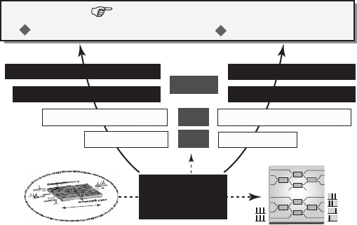
As a new topic of application, on the other hand, we proposed a unique research scheme by com-
bining QDs with another nanostructure, i.e. a photonic crystal (PC), to provide key photonic devices
for future advanced telecommunication systems, as shown in Fig. 17.1 [5] . In the left-hand wing is
an ultra-fast digital photonic network of the future, where an ultra-small and ultra-fast symmetri-
cal Mach–Zehnder (SMZ)-type [6] all-optical switch (PC-SMZ) has been developed so far in the fi rst
phase by using GaAs-based two-dimensional PC slab waveguides embedded with InAs-based QDs
( Fig. 17.1 ) [7] . In the second phase, the PC-SMZ is now evolving into a new functional key device, i.e.
an ultra-fast all-optical fl ip-fl op (PC-FF) device that is essential for the digital photonic network [5] .
CHAPTER 17
CH017-I046325.indd 529CH017-I046325.indd 529 6/25/2008 3:17:18 PM6/25/2008 3:17:18 PM
530 Handbook of Self Assembled Semiconductor Nanostructures for Novel Devices in Photonics and Electronics
As long as QD technology is concerned all through these two phases, a selective-area-growth
(SAG) of QDs has been shown to be an important subject for exhibiting an optical non-linear effect
in the selective optical non-linear arms particularly for the PC-SMZ and PC-FF. For this purpose,
a metal-mask (MM)/molecular beam epitaxy (MBE) method of InAs QDs has been developed [8] .
In the right-hand wing in Fig. 17.1 , on the other hand, another category of a future quantum
information system is described, where a single photon qubit composed of a single QD embed-
ded in a PC-based high- Q cavity is situated as another important product of the PC/QD-combined
nano-photonic structure [9–11] . The AFM-probe-assisted SCQD growth method mentioned above,
renamed recently as a nano-jet probe (NJP) method, has been developed for this purpose because of
its potential to position a single QD at the centre of the point defect PC high- Q cavity [12–14] .
Advanced telecommunication
Quantum information
Digital photonic network
Phase-2: All-optical flip-flop
Large ONL/phase shift
Wide/flat band
Phase-1: All-optical switch
Single photon qubit
Quantum entanglement
Site-controlled single dot
High-Q cavity
PC/QD
QD
PC
PC/QD
Nano-photonics
technologies
Matrix switch
PC-SMZ
~500 μm
Figure 17.1 Schematic research scenario of PC/QD combined nano-photonic structures for advance telecommuni-
cation systems.
In this chapter, two types of unique QD growth techniques have been reviewed. The MM
method for InAs QDs in the PC-based all-optical switching devices is shown in section 17.2 and
the advanced techniques for the growth of InAs SCQDs by using the NJP method is described in
section 17.3.
17.2 Selective-area-growth of InAs quantum dots using the metal-mask/MBE method
17.2.1 Introduction
A selective-area-growth (SAG) technique for self-assembled QDs is useful for various applications
of the QDs. In the case of our proposed all-optical devices, PC-SMZ [7] and PC-FF [5] , the SAG
technique is intensively required for their effective operations. For instance, although the embed-
ded QDs in the PC waveguides (WGs) of PC-SMZ act as a phase shifter due to their optical non-
linearity, the QDs simultaneously absorb the propagation light and result in a low transmittance
in the PC-WG. Therefore, the QD growth in limited regions in the WGs is desirable rather than an
entire growth on a substrate. Furthermore, the PC-FF, which composes two PC-SMZs, requires
SAG of two kinds of QDs having different absorption wavelengths for embedding the QDs in each
optical non-linearity arm in the PC-SMZs.
In this section, we describe a metal mask (MM)/MBE method [8] for SAG of self-assembled
InAs QDs. First, we introduce the MM/MBE method and characterizations of the SA-grown QDs
by atomic-force-microscopy (AFM) and photoluminescence (PL) measurements, including two-
dimensional (2D) PL intensity mapping. Successful SAG of InAs QDs was clearly demonstrated,
while the QD density and homogeneity were almost equal to those of the QDs grown without
the MM. Second, we describe technologies for controlling the PL wavelength of InAs QDs by
CH017-I046325.indd 530CH017-I046325.indd 530 6/25/2008 3:17:18 PM6/25/2008 3:17:18 PM
Advanced Growth Techniques of InAs-system Quantum Dots for Integrated Nanophotonic Circuits 531
using a strain-reducing-layer (SRL) [15] inserted on the QDs. Sequential variation of the PL peak
wavelength as a function of SRL thickness was attained by the SRL insertion method. Finally,
we report on fabrications of a PC-WG with SA-grown QDs. For avoiding refl ection due to a step
at a boundary of the selective growth area, we reduce the step height with a developed growth
sequence. Clear transmission spectra and pulse intensities/phase modulations in the PC-WG due
to the optical non-linearity of the QD are confi rmed.
17.2.2 Experimental apparatus and procedures for MM/MBE method
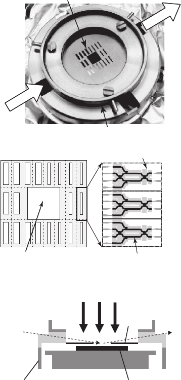
Figure 17.2a shows an image of the prepared MM attached on a holder. The tantalum (Ta) MM is
employed to cover undesired growth areas during conventional MBE growth. The MM holder can
be mounted on and off in an ultra-high vacuum (UHV) chamber without exposing the sample to
the atmosphere.
Large window for
RHEED observation
Selective growth area
(4 mm ⴛ 500 m)
PC-SMZ
(b)
Metal mask E-beam exit
E-beam
entrance
Metal mask holder
(a)
E-beam
GaAs substrate
MM
Sample holder
Molecular beams
(c) MM holder
Figure 17.2 (a) Photograph of a metal-mask (MM) holder. (b) Schematic of patterns on the MM designed for
PC-SMZ fabrications. (c) Cross-sectional illustration of the MM and e-beam incident for RHEED observations
during the MBE growth.
CH017-I046325.indd 531CH017-I046325.indd 531 6/25/2008 3:17:19 PM6/25/2008 3:17:19 PM
532 Handbook of Self Assembled Semiconductor Nanostructures for Novel Devices in Photonics and Electronics
As illustrated in Fig. 17.2b , the MM has a large window (6 mm 6 mm) at the centre and sev-
eral small windows of 4 mm 0.5–1.0 mm around it. The small windows are prepared for SAG
of QDs, suited for the PC-SMZ. On the other hand, the large window is used for RHEED (refl ection
high-energy electron-diffraction) observations and temperature measurements of the sample
surface by using a pyrometer during the MBE growth. An electron beam for RHEED observations
goes through the tunnels formed on the frame of the MM holder and is diffracted at the surface
where molecular beams are irradiated through the large open window during MBE growth, as
shown in Fig. 17.2c . These in situ observations enable us to optimize growth conditions for QDs.
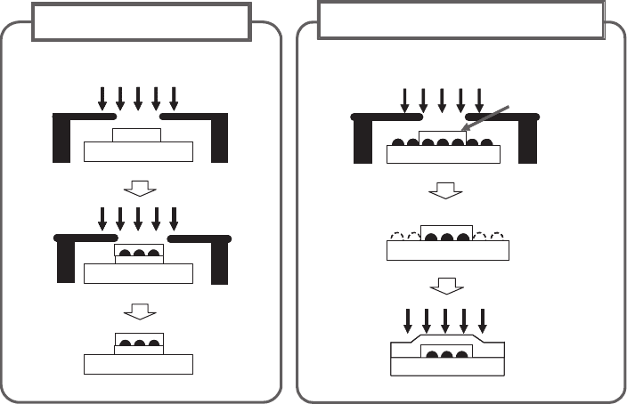
We have performed the SAG of the QD using two methods, i.e. “ mask ” and “ cap/anneal ” meth-
ods [16] , as schematically shown in Fig. 17.3 . In the mask method, QDs are grown when the
MM covers the substrate, namely the SAG of QDs is directly operated with the MM. In the cap/
anneal method, on the other hand, the MM is used for selective growth of capping layers of QDs
grown on the entire substrate. After the entire QDs ’ growth, a selective area GaAs layer is grown
by using the MM for capping selective area QDs, followed by an annealing to evaporate the rest of
the QDs.
Molecular beams
Molecular beams
Annealed
Mask
Cap/anneal
MM
MM
Capped
Figure 17.3 Two SAG sequences: “ mask ” and “ cap/anneal ” methods.
In both methods, sequences before QD growth are identical. At fi rst, a multilayer structure of
a 50 nm thick GaAs layer/30 nm thick Al
0.3
Ga
0.7
As layer/GaAs buffer layer was grown on the
entire GaAs substrate without the MM at approximately 540˚C. In the mask method, the MM
holder was then mounted after the sample was cooled down below 200˚C. Following this, the
sample was gradually heated up to the InAs QD growth temperature, typically 470–490˚C, and
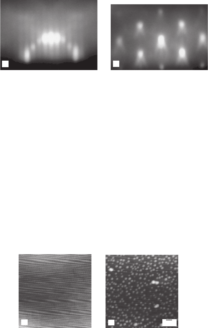
2.6 monolayers (ML) of InAs were deposited at a rate of 0.2 ML/s for the QD growth. During this
process, we confi rmed that the RHEED patterns varied from streaky to spotty patterns, as shown
in the photographs in Fig. 17.4a and b, respectively. A chevron pattern originated from the QD
facet, as shown in Fig. 17.4b , indicating 3D QD growth.
After the sample was slightly cooled down by approximately 40˚C to avoid the degradation of
the QD, a 3 nm thick In
0.2
Ga
0.8
As layer/3 nm thick GaAs cap layer was sequentially grown. In
the cap/anneal method, on the other hand, the InAs QDs were grown entirely on the GaAs layer
with a 2.6 monolayer (ML) InAs deposition at a rate of 0.2 ML/s without the MM. Then, the MM
was mounted on the sample after cooling down below 200˚C and the sample temperature was
CH017-I046325.indd 532CH017-I046325.indd 532 6/25/2008 3:17:19 PM6/25/2008 3:17:19 PM
Advanced Growth Techniques of InAs-system Quantum Dots for Integrated Nanophotonic Circuits 533
gradually raised up to typically 430–450˚C. Selective capping layers of 3 nm thick In
0.2
Ga
0.8
As
and 20 nm thick GaAs were grown at the temperature via the MM. After removing the MM, the
temperature of the sample was gradually raised up to the QD growth temperature, for instance
480˚C, and was kept for 3 min to evaporate the QDs on regions uncovered by the capping layer.
SAG of QDs was completed in this way. After SAG of QDs using both methods, a multilayer struc-
ture of 50 nm thick GaAs capping layer/30 nm thick Al
0.3
Ga
0.7
As layer/50 nm thick GaAs layer
was grown on the entire substrate. The Al
0.3
Ga
0.7
As layers were inserted below and above the QD
layer as an energy barrier against free carriers in the PL measurement of the QD. As mentioned
later, the capping layer of 3 nm thick In
0.2
Ga
0.8
As on the QD is employed for reducing the strain
in grown QDs and a red shift of the PL from QDs to around 1300 nm in wavelength.
17.2.3 Structural and optical properties of SA-grown Qds
We characterized the SA-grown QDs by AFM observations and PL measurements. Afterwards,
we showed results from samples grown by the mask method on behalf of the two SAG methods.
Figure 17.5 shows typical AFM images of regions masked and unmasked by the MM. The
image of an unmasked region shows formation of InAs QDs whose density is around 4 1 0
10
cm
2
, whereas no QD was formed on the masked regions of the surface. Such high density is
comparable to that of QDs conventionally grown without the MM. The mean lateral size and
height of the QD was approximately 40 nm and 5 nm, respectively.
Figure 17.4 RHEED patterns obtained (a) before and (b) after growth of QDs with the MM.
(a)
(b)
Masked region
(a)
Unmasked region
100nm
(b)
Figure 17.5 AFM images of masked and unmasked regions with the MM. SA-grown QDs with a density of
4 10
10
cm
2
were observed on the unmasked regions.
CH017-I046325.indd 533CH017-I046325.indd 533 6/25/2008 3:17:19 PM6/25/2008 3:17:19 PM
534 Handbook of Self Assembled Semiconductor Nanostructures for Novel Devices in Photonics and Electronics
For investigating the optical quality of SA-grown QDs, PL measurements were obtained at
room temperature (RT). An He–Ne laser ( λ 633 nm), focused to a diameter of several microns,
was used for QD excitation with a power of 80 μ W. A stepping-motor attached to the sample
stage was utilized for positioning the excitation area and 2D mapping of the PL intensity.
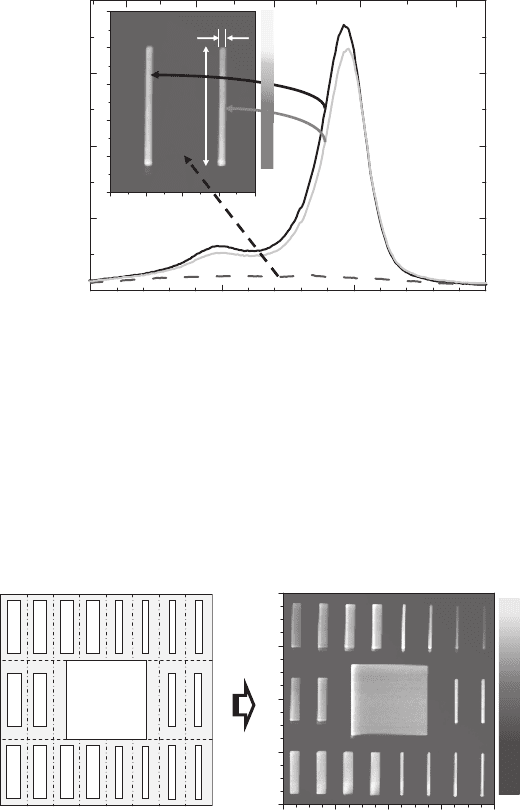
PL spectra and 2D intensity mapping from the unmasked and masked regions are shown in
Fig. 17.6 . The spectra shown with black and grey lines are measured from the unmasked regions
which are indicated in the PL intensity mapping by arrows. High contrast in the mapping shows
high PL intensity attributed to the SA-grown QDs. The PL peak and the FWHM are 1295 nm
(0.957 eV) and approximately 32 meV, respectively, which are almost the same as those of the
QDs grown without the MM. This small FWHM value obtained even at RT indicates the high
homogeneity of the SA-grown QDs comparable to that of QDs grown without the MM.
1100 1200 1300 1400
1.1 1.05 1 0.95 0.9
Photon energy (eV)
PL intensity (arb. unit)
Wavelen
g
th (nm)
021 3 4 (mm)
0
1
2
3
4
5
0
2.5E3
5.0E3
1.0E4
3.3mm
250om
7.5E3
3.3 mm
250μm
Figure 17.6 PL spectra and intensity mapping from SA-grown sample at room temperature.
0 4 8 12 16(mm)
0
4
8
12
16
0
2.5E3
5.0E3
7.5E3
1.0E4
Figure 17.7 PL intensity mapping image from the entire region under the MM. Successful SAG corresponding to
the MM pattern was confi rmed.
Moreover, these PL spectra measured at two different regions show almost identical intensity and
linewidth, suggesting that such high density and homogeneous QDs were grown on the selective
areas of the substrate independent of the position. On the other hand, no peak was found in the
PL spectrum from the masked region, as shown by a dashed line. Figure 17.7 shows a PL intensity
mapping of the entire masked and unmasked areas. Through these PL intensity mapping images,
the successful SAG of the entire region underneath the MM was clearly exhibited.
CH017-I046325.indd 534CH017-I046325.indd 534 6/25/2008 3:17:21 PM6/25/2008 3:17:21 PM
Advanced Growth Techniques of InAs-system Quantum Dots for Integrated Nanophotonic Circuits 535
Each QD-grown area decreased to approximately 0.25 m m 3.3 mm SAG area obtained from
a window size of 0.5 mm 4 mm. This shrinkage of the SAG area is considered to be due to ther-
mal evaporation of QDs near the edge of the windows by the heated MM.
17.2.4 PL wavelength control of InAs QDs with a strain-reducing-layer
As previously mentioned, successful SAG of QDs was attained by the MM/MBE method. However,
when applying the MM/MBE method to realize the PC-FF [5] , controlling absorption wavelength
of SA-grown QDs is also required. For that purpose, we inserted a strain-reducing-layer (SRL)
between QDs and spacers. This method is operated by covering grown QDs with an In
0.2
Ga
0.8
As
layer to reduce strain in the QDs, and it results in a red shift of the PL emission peak of QDs [15] .
We have investigated the effectiveness of the SRL for controlling the absorption wavelength of
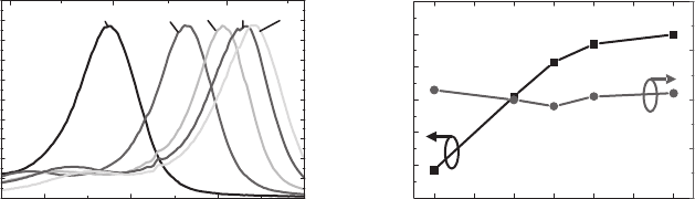
QDs. Figure 17.8a summarizes the PL spectra from strain-reduced QDs with different SRL thick-
nesses ranging from 0 to 6 nm. The PL spectra exhibit the PL peak wavelength that shifted from
1240 nm to 1320 nm and with the FWHM that was almost maintained at approximately 30 meV,
as shown in Fig. 17.8b .
1.05 1 0.95
1200 1250 1300 1350
PL intensity (arb. units)
Wavelength (nm)
SRL thickness: 0nm
2nm 3nm 4nm
6nm
Photon energy (eV)
0123456
1220
1240
1260
1280
1300
1320
1340
SRL thickness (nm)
PL peak wavelength (nm)
0
15
30
45
60
FWHM (meV)
(a)
(b)
Figure 17.8 Effectiveness of a strain-reducing-layer (SRL) for tuning the PL peak wavelength. (a) Summary of
PL spectra from QDs as a function of SRL thickness. (b) PL peak wavelength and FWHM variations against the SRL
thickness.
This result clearly indicates that the SRL can control the PL wavelength of QDs without degra-
dation of the QD optical quality. Thus, combination of the MM method and the insertion of the
SRL has a potential to develop the PC-FF, which requires SAG of QDs with different absorption
wavelengths at different areas.
17.2.5 Selective area-grown QD embedded in PC-WG
Here, we report on an application of the MM/MBE method to fabricate the SA grown QDs embed-
ded in PC-WGs. As previously mentioned, we developed the SAG technique for our proposed
PC-based devices. Considering an application of the SAG to PC-WGs, the step height of the SAG
area should be suppressed as much as possible since the step causes undesired refl ections of the
propagating light and narrowing the bandwidth of the transmitted light. Thus, we attempted to
minimize a step height of the SAG with optimizing the growth sequences. As a result, the SAG
method enables us to minimize the step height within 6 nm at the SAG region against the core
thickness 250 nm, as schematically shown in Fig. 17.9 . Also, we succeeded in characterizations
of the PC-WG with QDs partially embedded, i.e. the transmittance of the continuous wave (CW)
light and the intensity and phase modulations of light pulses due to the optical non-linear phe-
nomenon induced by the embedded QDs.
CH017-I046325.indd 535CH017-I046325.indd 535 6/25/2008 3:17:23 PM6/25/2008 3:17:23 PM
536 Handbook of Self Assembled Semiconductor Nanostructures for Novel Devices in Photonics and Electronics
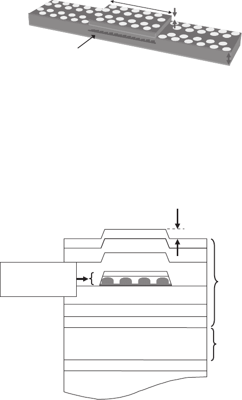
We prepared a GaAs-based straight PC-WG composed of an air bridge-type 2DPC slab and sin-
gle InAs QDs layer embedded in a selective area of the WG. Figure 17.10 shows a structure of the
MBE-grown sample for fabricating the PC-WG with SA-grown QDs. A 250 nm thickness GaAs
core layer with QDs on a 2 μ m thickness sacrifi cial clad layer was grown on a GaAs substrate. To
minimize the step height of the selective area, the MM was used for only QD layers and capping
layers of 6 nm in thickness.
InAs QDs
Core ~250nm
Step height ~6nm
SAG area
Figure 17.9 Schematic of PC-WG embedding SA-grown QDs. The ratio of a step height at SAG area to a core
thickness is below 2.4%, which should be negligible for pulse propagations.
GaAs 90 nm
Al
0.3
Ga
0.7
As 10 nm
GaAs 20 nm
GaAs (001)
GaAs buffer
Al
0.3
Ga
0.7
As 10 nm
GaAs 90 nm
GaAs 20 nm
Al
0.6
Ga
0.4
As 2000 nm
GaAs: 3 nm
In
0.2
Ga
0.8
As: 3 nm
InAs-QD: 2.6 ML
With MM
Step height 6nm
Core layer
~250 nm
Sacrificial layer
for air-bridge
~2 μm
Figure 17.10 MBE-grown sample structure for PC-WG with SA-grown QDs.
The MBE-grown sample was then transferred to electron beam lithography and dry etching
processes for fabricating the air bridge-type 2DPC slab [17] . The PC is constructed with holes of
hexagonal arrays. In the PC, a missing line of holes is prepared as a straight WG whose input and
output ports involve solid immersion lens and taper structures [18] resulting in a high coupling
effi ciency. By marking the position of SAG in advance, one can set the SA-grown QDs within the
WG. The lattice constant and radius of air holes are designed to include the centre wavelength of
the SA-grown QDs, around 1300 nm, within the transmission band of the WG.
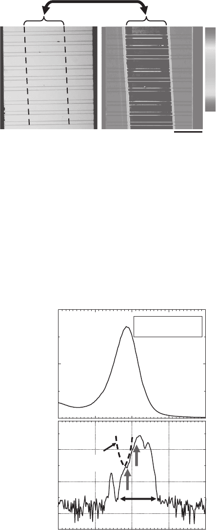
Figure 17.11a shows an optical microscope image of a fabricated sample. The area surrounded
by the dashed lines is embedded with the QDs. A PL intensity mapping obtained from the same
area in Fig. 17.11a exhibits clear PL emission of 1.29 μ m in wavelength from QDs embedded
in a selective area, as shown in Fig. 17.11b . These images indicate successful fabrication of the
PC-WG, embedding the SA grown QDs.
We then characterized the fabricated PC-WGs by CW transmission and pump/probe pulse
measurements. The transmission spectra were observed with CW white light as a light source
CH017-I046325.indd 536CH017-I046325.indd 536 6/25/2008 3:17:24 PM6/25/2008 3:17:24 PM
Advanced Growth Techniques of InAs-system Quantum Dots for Integrated Nanophotonic Circuits 537
and a conventional measurement set-up. Figure 17.12b shows the transmission spectra obtained
from the PC-WG. The transmission band through the WG mode is seen from 1270 nm to
1330 nm indicated by a black arrow. This value almost corresponds to the transmission band of
the straight WG without QDs, therefore, the step height of the SAG area, below 6 nm, should not
infl uence the transmission. An absorption attributed to the QDs is observed around 1290 nm, as
depicted by a dashed line, corresponding to the inverse of the PL spectrum shown in Fig. 17.12a .
From the above results, we confi rmed a successful fabrication of the PC-WG embedding the
SA-grown QDs; the transmission band was set to include the QD absorption centre wavelength,
while no infl uence of the step height was observed.
0
0.3
0.5
0.8
1
PL intensity (a.u.)
500 μm
(a) (b)
SA-grown QD area
Figure 17.11 (a) Optical microscope image of a fabricated sample with PC/QD straight WGs. (b) PL intensity
mapping from the sample. PL intensity of 1290 nm in peak wavelength due to the SA-grown QDs is clearly shown.
Figure 17.12 (a) PL spectrum from the SA-grown QDs at RT. (b) The transmission spectrum obtained from the
PC/QD WG.
PL intensity (arb. unit)
Peak : 1292 nm
FWHM: 29.3 meV
@RT
1200 1250 1300 1350 1400
50
40
30
Intensity (dB)
Wavelength (nm)
(a)
(b)
pump
probe
PC-WG
Absorption
by QDs
CH017-I046325.indd 537CH017-I046325.indd 537 6/25/2008 3:17:25 PM6/25/2008 3:17:25 PM
538 Handbook of Self Assembled Semiconductor Nanostructures for Novel Devices in Photonics and Electronics
Then, we measured the non-linear phenomena by the QD, amplitude and phase shift of signal
pulses (SPs) induced by control pulses (CPs), which are essential for the operation of PC-SMZ.
The optical non-linearity-induced modulations were measured by utilizing a two-colour pump
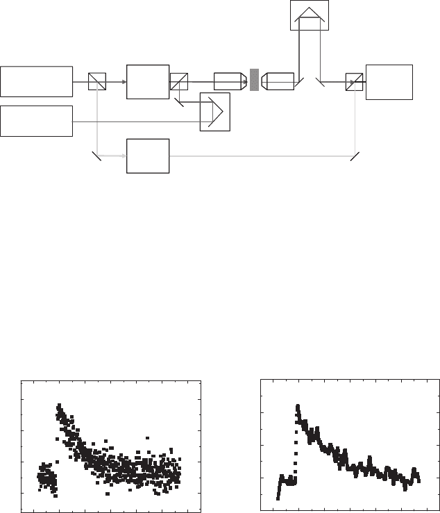
and probe set-up, as shown in Fig. 17.13 [7] .
Probe
AOM1
AOM2
OPO (probe)
Delay
Sample
Reference
Pump
BS
OPO (pump)
Delay
PIN PD
BS
Figure 17.13 Schematic of the experimental apparatus for two-colour pump/probe measurements.
The SPs and CPs were collinearly coupled into the PC-WG. By considering the transmission
spectrum shown in Fig. 17.12b , we set the CPs ’ centre wavelength to the centre of the QDs ’
absorption wavelength, 1290 nm, and set the SPs ’ centre wavelength to a longer wavelength,
1310 nm. The ONL-induced amplitude and phase shifts of the SPs were measured by lock-in-
based heterodyne detection. Figure 17.14 shows typical non-linearity-induced amplitude and
phase modulations of SP against time delay between the CP and the SP. The shift of the ampli-
tude and the phase of SPs due to the CPs were clearly observed. The energies of the SP and the
CP in the WG were estimated to be 33.8 fJ/pulse and 338 fJ/pulse, respectively. The net energy is
estimated from the coupling effi ciency into the PC-WG.
100 0 100 200 300 400 500
0.5
0.0
0.5
1.0
ΔAmp. (a. u.)
CP/SP delay (ps)
100 0 100 200 300 400 500
20
0
20
40
60
Phase shift (deg)
CP/SP delay (ps)
Figure 17.14 The ONL-induced amplitude and phase shifts of SPs against time delay between CPs and SPs.
In this case, we have obtained the phase shift value around 45°. This value is consistent with
that previously obtained from the sample with entire-grown three-layer-stacked QDs, e.g. 130°
[7] , considering that this sample includes a single layer of QDs. However, for PC-SMZ operations,
which requires the SP phase shift of at least 180°, further improvement of the non-linearity effi -
ciency is necessary, e.g. by QD stacking growth or utilizing the slow light in the hetero V
g
(group
velocity) PC-WG [19] .
17.2.6 Summary
We have succeeded in the SAG of InAs QDs by the developed MM/MBE method. The SA-grown
QDs, which exhibit comparable structural and optical qualities with conventional QDs grown
CH017-I046325.indd 538CH017-I046325.indd 538 6/25/2008 3:17:26 PM6/25/2008 3:17:26 PM