Henini M. Handbook of Self Assembled Semiconductor Nanostructures for Novel devices in Photonics and Electronics
Подождите немного. Документ загружается.

Advanced Growth Techniques of InAs-system Quantum Dots for Integrated Nanophotonic Circuits 539
without the MM, can be utilized in PC-SMZ. The PL peak wavelength was red shifted with a
strain-reducing-layer from 1240 nm to 1320 nm with the SRL thickness. The combination of
these techniques is promising for realizing an all-optical digital fl ip-fl op device: PC-FF.
In addition, we have fabricated the PC-WG embedding SA-grown QDs. The non-linearity-
induced amplitude and phase shifts of signal pulses due to the control pulses were confi rmed.
Although the embedded QD layer was single, around a 45° phase shift was observed. More non-
linearity effi ciency improvements, by such as multilayer QD stacking and utilization of slow light,
enable us to obtain suffi cient phase shift value for the switch operation in PC-SMZ. These results
indicate that the SAG technique can be applied to fabricate the PC-WG with QDs partially embed-
ded for PC-SMZ and PC-FF.
17.3 Site control of InAs QDs using the nano-jet probe (NJP)
17.3.1 Introduction
In the previous section, we reported on a selective-area-growth (SAG) technique involving self-
assembled InAs QDs that uses an in situ metal mask (MM). This MM method is a simple technique
to obtain high-quality InAs QDs in selected areas for PC-SMZ and PC-FF by merely positioning
shadow masks on the sample surface. However, the QDs fabricated by the MM method are ran-
domly distributed on the sample surface, since their growth proceeds in the Stranski–Krastanov
(SK) mode. In other words, the MM method cannot control the nucleation sites of the QDs pre-
cisely. If the nucleation sites can be intentionally controlled on a nanometre scale, then the QDs
can be arranged hexagonally on the sample surface. This is the best way to obtain a high den-
sity of QDs. Additionally, Lee et al. pointed out in their calculation that the uniformity of QDs
can be improved by growth on sample surfaces containing regularly arranged nucleation sites
[20] . Furthermore, considering the application of QDs to cavity quantum electrodynamics (QED)
devices such as single-photon emitters, which comprise QDs embedded in a photonic crystal
(PC)-based cavity [10, 11] , controlling the nucleation sites of QDs is one of the key issues since
the position of the QDs determines the performance of the devices.
In this section, we report on an advanced technique for obtaining site-controlled QDs that ena-
bles the formation of the required number of QDs at the desired locations. In previous papers,
we reported a scanning-tunnelling-microscope (STM)-probe-assisted site-control technique for
InAs QDs and demonstrated the formation of two-dimensionally (2D) arrayed QDs with differ-
ent constant (50 100 nm) pitches [3] . However, when we consider applying this method to
our recently proposed PC-based all-optical switches [5] , which require many uniform QDs in the
selected areas, the capability of the reported method for selective QD formation using the STM
probe is not suffi cient for practical nanofabrication use since the throughput of this technique
is 0.5–1 s/dot. Furthermore, a change in the shape of the apex of the STM tip during the fabri-
cation process is an inevitable problem since this technique utilizes a part of the tip itself as a
depositing material for creating the nucleation sites of QDs [3] .
To solve these problems, we have recently proposed a new technique that employs an in situ
AFM probe with a specially designed cantilever, which is referred to as the nano-jet probe (NJP)
[12, 21] . The NJP provides the capability to fabricate high-density 2D indium (In) nano-dot
arrays on GaAs substrates within a selected area; these arrays can be directly converted into InAs
arrays by subsequent annealing with arsenic fl ux irradiation [4] . Using this method, we have
achieved site-controlled QD formation at desired locations on the sample surface [22] .
17.3.2 Experimental apparatus and procedures
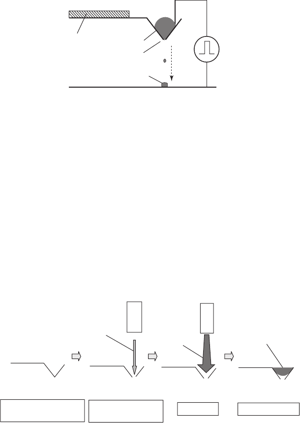
Figure 17.15 shows a schematic illustration of the micro-fabricated cantilever (NJP) and the
procedure for nano-dot formation developed in this study. The nano-dot formation was realized
using a UHV-AFM probe with a specially designed cantilever. The probe had a hollow pyramidal
tip with a submicron-sized aperture on the apex and an In-reservoir tank within the stylus. This
cantilever belongs to the piezoelectric type, and it is used for nano-dot fabrication as well as for
CH017-I046325.indd 539CH017-I046325.indd 539 6/25/2008 3:17:27 PM6/25/2008 3:17:27 PM
540 Handbook of Self Assembled Semiconductor Nanostructures for Novel Devices in Photonics and Electronics
sensing the force in AFM observations. The nano-dot formation was performed in a non-contact
mode. By applying a voltage pulse between the pyramidal tip and the sample, In clusters were
extracted from the reservoir tank within the stylus through the aperture, resulting in In nano-
dot formation.
Electric
pulse
Cantilever
PZT
Pyramidal tip
In dot
Aperture
In
Substrate
Figure 17.15 Schematic illustration of the NJP and the procedures involved in nano-dot formation.
Figure 17.16 shows the fabrication process of the cantilever developed in this study. We used
a commercially available batch-fabricated silicon cantilever with a hollow pyramidal stylus.
The developed cantilever was embedded with a lead zirconate titanate (PZT) piezoelectric thin
fi lm on its beam, sensing the force during AFM observations as well as actuating. The cantilever
for nano-dot formation was prepared as follows. First, a submicron-sized aperture was formed
on the apex of the stylus using a focused ion beam (FIB) system (SIM 9200: Seiko Instruments
Inc.) with a Ga
ion beam operating at 30 kV. The beam diameter was approximately 50 nm at
300 pA. The typical diameter of the aperture was approximately 500 nm and this diameter can
be reduced to a few tens of nanometres by focusing the ion beam on the irradiated region. The
measured mechanical resonance frequency of the cantilever is 80–100 kHz and the calculated
spring constant is approximately 150 N/m. Next, In was deposited into the hollow stylus from
the opposite side by an evaporator operated in high vacuum. The average thickness of the depos-
ited In layer was of the order of a few microns. The amount of charged In is suffi cient to form at
least one million In nano-dots.
Ion gun
In evaporator
In beam
Ion beam
Charged in
Nano-jet probe
In charge
Formation of micro-
aperture
Cantilever with hollow
pyramidal tip
Fabricated by batch
process
(commercially available)
Focused ion beam
etching
Deposition of In into
the reservoir tank
within the pyramidal
tip
Figure 17.16 Schematic illustration of the fabrication processes of the NJP.
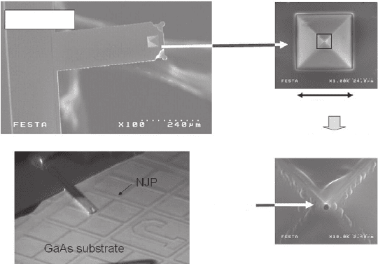
Figure 17.17 shows the scanning electron microscope (SEM) images of the fabricated canti-
lever and a long-distance optical microscope image of the NJP, which is located above the sample
surface. The length and width of the cantilever beam are approximately 500 µm and 150 μ m,
CH017-I046325.indd 540CH017-I046325.indd 540 6/25/2008 3:17:27 PM6/25/2008 3:17:27 PM
Advanced Growth Techniques of InAs-system Quantum Dots for Integrated Nanophotonic Circuits 541
respectively. The pyramidal tip integrated at the end of the beam has a base area of approxi-
mately 50 μ m
2
and is approximately 30 μ m in height; a submicron-sized aperture is situated
at the apex of the stylus. In the SEM image of the close-up view, as shown in Fig. 17.17, a
submicron-sized aperture can be observed at the apex of the stylus.
Figure 17.17 Scanning electron microscope images and long-distance optical microscope image of the NJP. (a) The
entire image of the cantilever. (b) A high magnifi cation image of the pyramidal tip. (c) A close-up view of the apex
of the pyramidal stylus (a submicron-sized aperture can be observed at the apex in the image). (d) A long-distance
microscope image of the NJP, which is located above the patterned GaAs substrate.
Cantilever (NJP)
SEM image
Pyramidal tip
Point of pyramidal stylus
(close-up view)
Aperture
∼subμm
50 μm
The experiments of In nano-dot formation were performed with a conventional UHV-AFM
(made by Unisoku Co. Ltd). Considering the application for mass production use which requires the
deposition of In dots on a large area, our AFM system has a linear motion scanning stage with a
range of 100 μ m 1 0 0 μ m and a capacitive feedback sensor for high accuracy and repeatability
in the sub-nanometre range. This stage enables the precise positioning of the nano-dot formation
as well as large-area scanning in the AFM observation after the deposition of nano-dots. Further,
a pulsed voltage of either polarity under 150 V for 0.1 ms–1000 ms can be applied to the stylus at
any position on the sample within the large scanning range by employing computer control.
Our apparatus has a specially designed tip-repositioning function. This function enables us to
repeatedly observe AFM images of identical nanostructures with ease, even after demounting the
sample holder from the AFM unit and remounting it. For this purpose, a long-distance optical
microscope was used for monitoring the approach of the probe on the sample surface through a
viewport of the AFM chamber. Additionally, mesa-array-patterned substrates (typically 400 μ m
2
mesa, as shown in Fig. 17.17 ), which were prepared by the conventional photolithography tech-
nique, were used for the coarse positioning of the AFM probe. Since the optical microscope has
a high resolution, it allowed the probe to be accurately positioned at the centre of the specifi ed
mesa top surface. Subsequently, the large scanning area of the piezoelectric scanner (100 µm
2
)
enabled us to easily identify the target nanostructures such as the QDs, which had been formed
around the centre of the mesa. Using this function, a step-by-step evaluation of SC QDs is avail-
able at each point during the MBE growth, AFM observation, and In nano-dot fabrication.
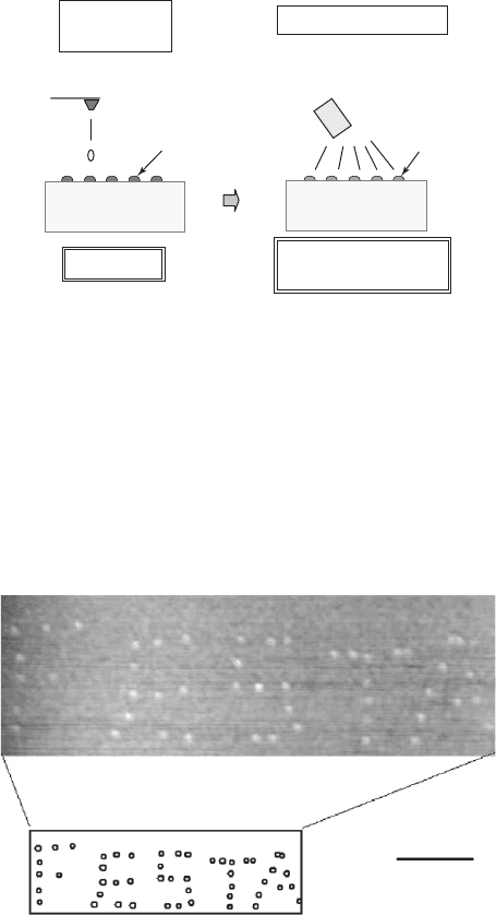
17.3.3 Fabrication of site-controlled QDs
17.3.3.1 In nano-dot formation
Figure 17.18 shows a series of the illustrations for the experimental procedures involved. The
fi rst step is the In nano-dot deposition and the second is the crystallization process of the In
CH017-I046325.indd 541CH017-I046325.indd 541 6/25/2008 3:17:28 PM6/25/2008 3:17:28 PM
542 Handbook of Self Assembled Semiconductor Nanostructures for Novel Devices in Photonics and Electronics
nano-dots into the InAs QDs using the droplet epitaxy technique. In order to deposit nano-dots, a
single voltage pulse was applied between the tip and the GaAs substrate using an AFM operated
in the non-contact mode at room temperature. Here, the magnitude of the pulsed voltage was
defi ned as the value applied to the substrate (with the tip grounded). The value of the applied
pulsed voltage for the nano-dot formation varied in the range of 70–140 V, although it was some-
what dependent on the cantilever. During the deposition, the feedback loop was turned off and
no additional bias voltage was applied between the tip and the sample. After the deposition, the
AFM images were observed using the same tip that was used for the deposition of the nano-dots.
In nano-dot
formation
Conversion to InAs
As-irradiation
with annealing
InAs
In deposition
at RT
NJP
UHV-AFM
Using droplet
epitaxy technique
GaAs
GaAs
Figure 17.18 Schematic illustrations of the site-controlled formation processes for InAs QD structures using the
NJP method.
500 nm
Figure 17.19 AFM image of an In nano-dot pattern ( “ FESTA ” ) deposited on an Si substrate. The deformed pattern
of the “ FESTA ” with a rather large pitch ( 100 nm) is caused by hand patterning for a preliminary study.
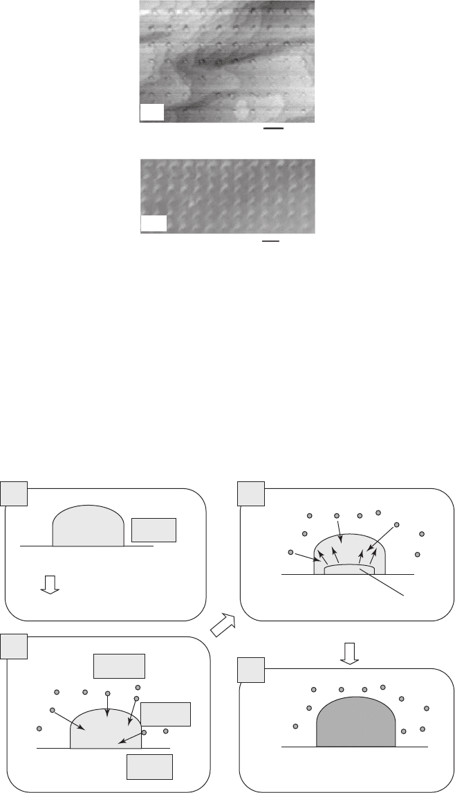
Figure 17.19 shows the AFM image of an In nano-dot pattern deposited on an Si surface for a
preliminary study. Each dot was formed by applying an electric pulse of 75 V for 7 ms between the
tip and the sample. The typical diameter of the formed dots was 30–40 nm in diameter. Although
the dots are rough in pitch and disordered, an intentionally patterned word “ FESTA ” can be rec-
ognized in the AFM image. The deformation in the pattern was caused due to the positioning of
each dot by hand, and it can be easily improved with regard to the order and pitch by moving the
cantilever using computer control.
The success of the In nano-dot formation depends on parameters such as the voltage, the width
and shape of the applied electric pulse, and the distance between the tip and the sample during
the deposition. Further, the size of the In nano-dots increases with the applied voltage pulse.
CH017-I046325.indd 542CH017-I046325.indd 542 6/25/2008 3:17:29 PM6/25/2008 3:17:29 PM
Advanced Growth Techniques of InAs-system Quantum Dots for Integrated Nanophotonic Circuits 543
There is a likelihood that In nano-dot formation has a threshold for the applied pulsed voltage.
The threshold value for forming the nano-dots, which is somewhat dependent on the cantilever,
usually varied between 70 and 120 V. This threshold value is considerably larger when compared
to the results reported previously by other researchers [23, 24] .
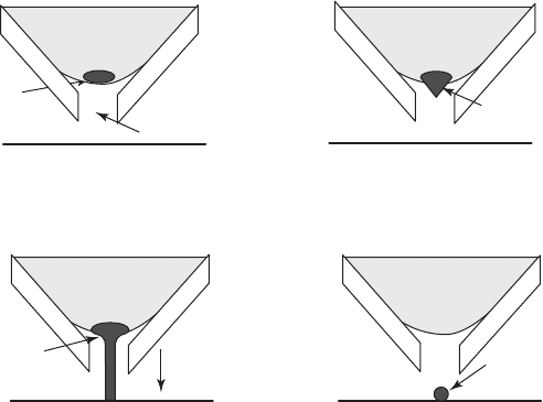
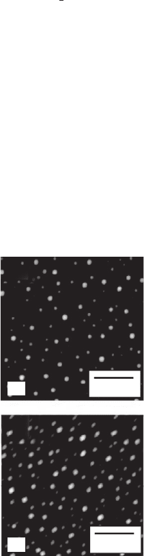
Figure 17.20 shows one possible mechanism of the In nano-dot formation. The top of the
In mount is actually positioned approximately 1 μ m inside the aperture since the thickness of
the walls of the pyramidal tip is around 1 μ m. Additionally, the distance between the top of the
pyramidal tip and the sample is around 10 nm since the AFM is operated in the non-contact
mode. After moving the tip closer to the sample, we applied a pulsed voltage between the tip and
the sample. In the early stage of deposition, local melting of In due to fi eld evaporation caused by
high applied voltage [25] may occur on the top of the In mount ( Fig. 17.20a ). A small protrusion
of In may then be formed in the next stage of deposition ( Fig. 17.20b ). In the subsequent stage
of deposition, this protrusion is elongated by the strong electric fi eld, and the melted In forms a
so-called Taylor cone due to the equilibrium between the electrical and the surface tension forces
[26] . Finally, an In droplet is separated from the bridge and an In nano-dot is formed on the sub-
strate. Although the details of the mechanism involved in the In nano-dot formation are unclear,
the mechanism of the In nano-dot formation is thought to be similar to that of an electric droplet
ejection in inkjet patterning [27] .
Local melting
Sub.
Aperture
Protrusion
Sub.
Sub.Sub.
Taylor cone
(c) (d)
(a) (b)
Nano-dot
E
In In
InIn
Figure 17.20 Schematic illustrations of the possible mechanism of nano-dot formation.
The size of the In nano-dots does not depend on the aperture size, that is, the In nano-dots
are considerably smaller when compared to the aperture, the diameter of which is typically
30–50 nm. In nano-dots of nearly constant size were formed for aperture sizes of 1 μ m, 500 nm
and 200 nm. These results can be explained by the limitations on the extent of the melting of
In on the top of the In mount since the melting area is determined by the applied voltage rather
than the aperture size.
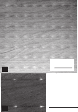
Figure 17.21a shows the AFM image of a fabricated 2D In nano-dot array with periods of
1 μ m deposited on a GaAs substrate. Each nano-dot was generated by the application of a single
voltage pulse of 120 V for 10 ms. In the AFM image, each observed nano-dot does not possess
a clear shape. This is likely to be a tip-induced artifact. In the case of the NJP, the point of the
top apex of the pyramidal tip was removed in order to form the micro-aperture. As a result, the
blunt tip sometimes causes the artifact observed in the AFM image. However, in certain cases,
the resolution of the AFM image improves despite the use of the same tip. Figure 17.21b shows
CH017-I046325.indd 543CH017-I046325.indd 543 6/25/2008 3:17:30 PM6/25/2008 3:17:30 PM
544 Handbook of Self Assembled Semiconductor Nanostructures for Novel Devices in Photonics and Electronics
an AFM image of the same sample at higher magnifi cation. In this image, a clear nano-dot shape
is observed. This image is considered to be produced by a coincidental protrusion formed around
the apex of the tip during scanning. These results suggest that the AFM image observed using the
NJP does not always refl ect the real shape of the nano-dots. Therefore, STM or AFM observations
employing a conventional tip should be used for the precise characterization of the nano-dots.
Nevertheless, the NJP is suffi ciently capable of recognizing whether or not the nano-dot has been
successfully formed.
2 μm
1 μm
(a)
(b)
Figure 17.21 AFM images of an In nano-dot array deposited on a GaAs substrate. The spacing between each nano-
dot is 1 μm. Image (b) shows a higher magnifi cation of the upper-left region of (a).
Figure 17.22 shows the AFM images of 2D In nano-dot arrays with periods of 100 nm and
50 nm deposited on GaAs substrates. Each nano-dot was formed on an MBE-grown GaAs sur-
face by applying a single voltage pulse of 140 V for 10 ms. In Fig. 17.22a , GaAs surface steps
produced during MBE growth were observed on the sample in addition to In nano-dots. The sur-
face density of the In nano-dots shown in Fig. 17.22b correspond to 4 1 0
10
cm
2
, which sat-
isfi es the requirements of the device fabrication from the viewpoint of the QD surface density.
Although, in this case, it took approximately 2 min to form 20 20 In nano-dots (corresponding
to approximately 3 dots/s), a throughput of 20 dots/s was achieved by optimizing the fabrication
conditions. This throughput (corresponding to 10 000 In nano-dots formed in approximately
10 min) is considered to be suffi cient for use in mass production.
In the AFM images shown in Figs. 17.21 and 17.22 , there seems to be some non-uniformity
in the dots. However, the precise determination of this fl uctuation is diffi cult at present because
of the poor resolution of the NJP for inspection, as mentioned in the previous section. The In
nano-dot array formation was demonstrated for a preliminary study. Therefore, fl uctuations
in the position, size, and shape of the In nano-dot arrays can be decreased by further optimization
of the conditions for nano-dot formation.
17.3.3.2 InAs conversion process
The ordered In nano-dots are directly converted into InAs QD arrays by subsequent irradiation
with arsenic fl ux in the MBE chamber which is connected to the AFM chamber through a UHV
tunnel. The droplet epitaxy technique makes it possible to crystallize In nano-dots into InAs dots.
This technique was proposed by Chikyow and Koguchi, who deposited Ga droplets on an AlGaAs
surface and then converted them to GaAs dots by annealing with As fl ux [28] . We applied
CH017-I046325.indd 544CH017-I046325.indd 544 6/25/2008 3:17:30 PM6/25/2008 3:17:30 PM
Advanced Growth Techniques of InAs-system Quantum Dots for Integrated Nanophotonic Circuits 545
this technique to the process of converting In nano-dots into InAs dots. The crystallization of
In nano-dots into InAs dots can be attributed to a vapour–liquid–solid (VLS) mechanism [29, 30] .
The annealing process with As fl ux incorporates As atoms into melted In, resulting in the crys-
tallization of InAs. Figure 17.23 shows schematic illustrations of the conversion mechanism of
In droplets into InAs dots.
100 nm
50 nm
(a)
(b)
Figure 17.22 AFM images of high-density In nano-dot arrays deposited on an MBE-grown GaAs surface. The
spacing between the In nano-dots is (a) 100 nm and (b) 50 nm. The surface density of the In nano-dots for each
sample corresponds to 1 10
10
cm
2
and 4 10
10
cm
2
, respectively.
I III
II
IV
Solid
Solid
GaAs
GaAs
GaAs
GaAs
As
AsAs
Liquid
Vapour
In
In
In
InAS
Annealing
with As flux
InAs
Growth of InAs crystal in the In droplet
Arsenic incorporation into the In droplet
InAs dot formation
Figure 17.23 Schematic illustrations of the conversion mechanism of In droplets into InAs dots.
CH017-I046325.indd 545CH017-I046325.indd 545 6/25/2008 3:17:30 PM6/25/2008 3:17:30 PM
546 Handbook of Self Assembled Semiconductor Nanostructures for Novel Devices in Photonics and Electronics
Before applying this technique to the process of converting In nano-dots into InAs dots, the crys-
tallization process was investigated by using In droplets, which were formed by the conventional
MBE technique. The sample was prepared by the deposition of 3 ML of In at 200°C on a GaAs
(2 4) reconstructed surface, which was terminated by the deposition of 0.75 ML of Ga atoms.
An AFM image of the sample prepared in this manner revealed the In droplet formation ( Fig.
17.24a ). The annealing condition was optimized using the In droplets formed by this procedure.
The temperature of the sample was gradually increased (10°C/min) up to 400°C under an arsenic
fl ux pressure of 5 1 0
5
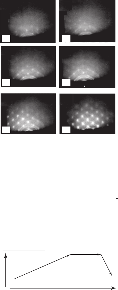
Torr, after which the sample was annealed for 20 min. Figure 17.25
shows the typical RHEED patterns along the
[]11 0
direction during the crystallization process of
the In droplets. Arsenic fl ux was irradiated before increasing the substrate temperature. A diffused
spotty pattern was observed before the annealing started ( Fig. 17.25a ). This means that a part
of the In droplets was crystallized at room temperature (below the melting point). This diffused
spotty pattern gradually changed to a clear spotty one as the substrate temperature increased.
Additionally, a clear ring pattern appeared when the substrate temperature increased above 200°C
( Fig. 17.25c ), indicating poly-crystal formation on the sample. This means that the crystallization
process of In droplets is incorporated with the poly-crystal formation. Spotty and ring patterns
continued to coexist until the substrate temperature reached 400°C. Finally, when the substrate
temperature exceeded 400°C, the ring pattern disappeared and the RHEED patterns showed only
clear spotty patterns with extended streaks, indicating that the crystallization process was com-
pleted. In addition, facets were formed on the converted InAs dots ( Fig. 17.25f ). The AFM image
of the converted In droplets is shown in Fig. 17.24b . The crystallization of In nano-dots formed by
the NJP was performed under the same conditions as those for the optimized one investigated by
using In droplets.
(a)
(b)
500 nm
500 nm
Figure 17.24 AFM images of In droplets (a) before and (b) after the crystallization process.
The actual conversion process was performed as follows. After the In nano-dots were depos-
ited, the sample was transferred to the MBE chamber to crystallize them. Figure 17.26 shows
the time sequence for the crystallization process. The temperature of the sample was gradually
raised to 420°C under an arsenic fl ux of 5 1 0
5
torr and the sample was annealed for 40 min.
Subsequently, it was transferred to the AFM chamber and its surface structure was observed by
AFM. In order to identify the region where the In nano-dots were deposited, the tip-repositioning
system, which was mentioned in the previous section, was used. The AFM image revealed the
CH017-I046325.indd 546CH017-I046325.indd 546 6/25/2008 3:17:31 PM6/25/2008 3:17:31 PM
Advanced Growth Techniques of InAs-system Quantum Dots for Integrated Nanophotonic Circuits 547
formation of InAs nano-dot arrays at the same position where the In nano-dots had been depos-
ited. Figure 17.27 shows the AFM images and schematic illustrations of the nano-dots before
and after the conversion. Before the conversion, the In nano-dots appeared cone shaped, as
shown in Fig. 17.27a . After the conversion, however, they assumed anisotropic shapes, as shown
in Fig. 17.27b . To be precise, the nano-dots were elongated along the
[]11 0
direction after the
conversion. Additionally, high-index facets were formed on the side walls of the converted nano-
dots ( Fig. 17.27c ). These features of the converted nano-dots correspond to those of the InAs
self-assembled QDs. Therefore, based on these observed changes in the features of the nano-dots,
we concluded that the In nano-dots had been converted into InAs dots.
(a)
(c) (d)
(e)
(b)
(f)
Figure 17.25 RHEED images during the InAs conversion process using In droplets formed by the conventional
method. The substrate temperatures are (a) room temperature before annealing, (b) 85°C, (c) 210°C, (d) 265°C,
(e) 360°C, and (f) 400°C.
420°C 40 min
10°C/min
As flux:
510
5
torr
Time
Tg
RT
Annealing sequence
Figure 17.26 Time sequence for the crystallization process.
17.3.3.3 Stacking of ordered InAs QDs
As the next step, we stacked InAs QDs using the converted InAs dots as the template. Figure
17.28 shows schematic illustrations of the experimental procedures. First, by using the NJP,
we fabricated 2D In nano-dot arrays ( Fig. 17.28a ). Then, in order to convert these ordered In
nano-dot arrays to InAs QDs, the sample was transferred to the MBE chamber through the
UHV tunnel and was subsequently annealed by irradiation with arsenic fl ux ( Fig. 17.28b ).
CH017-I046325.indd 547CH017-I046325.indd 547 6/25/2008 3:17:32 PM6/25/2008 3:17:32 PM
548 Handbook of Self Assembled Semiconductor Nanostructures for Novel Devices in Photonics and Electronics
Subsequently, self-assembled InAs QDs were grown on the converted InAs 2D arrays. We grew a
10 nm thick GaAs layer and deposited 1.4 ML of InAs on the converted InAs QD arrays; the sur-
faces were then observed by AFM ( Fig. 17.28c ). Figure 17.29 shows a typical AFM image of a 2D
In nano-dot array fabricated by the NJP method. The typical size of the In nano-dots is approxi-
mately 40 nm and their height was approximately 3–4 nm. In nano-dots were deposited in the
area of approximately 4 μ m 4 μ m with periods of 200 nm, as shown in the inset of Fig 17.29 .
GaAs (001) Sub.
GaAs (001) Sub.
(110)
(110)
(110)
(110)
(110)
(a) (b)
(c)
Figure 17.27 AFM images of the In nano-dots (a) before and (b) after the crystallization process. Image (c) is a
3D close-up view of the converted InAs dot.
In nano-dot
array formation
Conversion to InAs
at RT
In deposition
As-irradiation
with annealing
InAs
GaAs
GaAs GaAs
GaAs Cap and
2nd QD growth
AFM observation
(a) (b) (c)
Figure 17.28 Fabrication process of stacked InAs QDs using In(As) dot arrays formed by the NJP method as
templates.
Figure 17.30 shows an AFM image of the InAs-deposited GaAs surface, which is stacked on
the converted InAs dots. The AFM image revealed the selective formation of high-density InAs
dots only in the square region where the In nano-dots were formed by the NJP method. Despite
taking into account the deformation effect due to the blunt shape of the NJP, the size of the InAs
dots thus formed is large compared to the InAs QDs grown by the conventional SK mode. The
increase in the density of the InAs dots and their large size were probably due to the thin GaAs
covered layer and a large amount of InAs deposition, that is, a QD on the fi rst layer generates a
CH017-I046325.indd 548CH017-I046325.indd 548 6/25/2008 3:17:33 PM6/25/2008 3:17:33 PM