Middleton W.M. (ed.) Reference Data for Engineers: Radio, Electronics, Computer and Communications
Подождите немного. Документ загружается.

32-38
REFERENCE
DATA
FOR ENGINEERS
For example, for spacings smaller than 0.9375h, only
one beam exists, and for most spacings it is a back-
ward-directed beam. Multiple beams are, of course,
undesirable; this type of plot enables the single-beam
range to be quickly discovered. It is necessary to
inspect beam behavior over the entire frequency band
of interest, which can be done with other types of
plots.” Change of beam angle with frequency is impor-
tant and can readily be written in a normalized form:
f[(d/dj-)(sin
So)]
=
l/(P/k)
-
sin
0,
It can be seen that the normalized slope depends sim-
ply on
Pik
and the beam angle.
Corporate feeds can be used with a linear array;
power dividers or hybrid junctions can usually provide
significantly greater bandwidth than the array ele-
ments. Thus, for wideband arrays corporate feeds
are
recommended. However, corporate feeds are generally
bulky and expensive except for implementation in
stripline or microslrip. Thus, printed-circuit arrays are
often built with corporate feed networks.
Mutual Impedance
Mutual impedance between elements in any array
affects both fixed beam and scanning arrays.
In
the
former, the mutual impedance effects can be accom-
modated in the design of the array.? Arrays of medium
gain elements such as horns, spirals, or dishes may
exhibit only minor mutual coupling effects. However,
scanning with such large virtual subarrays is severely
limited due to quantization lobes (see the subsection
on electronic scanning in this chapter). Mutual imped-
ance between low-gain elements is typified by that of
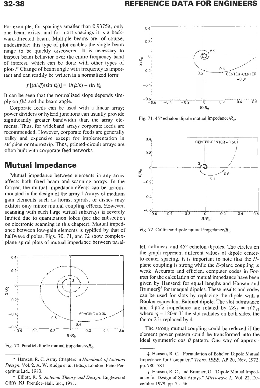
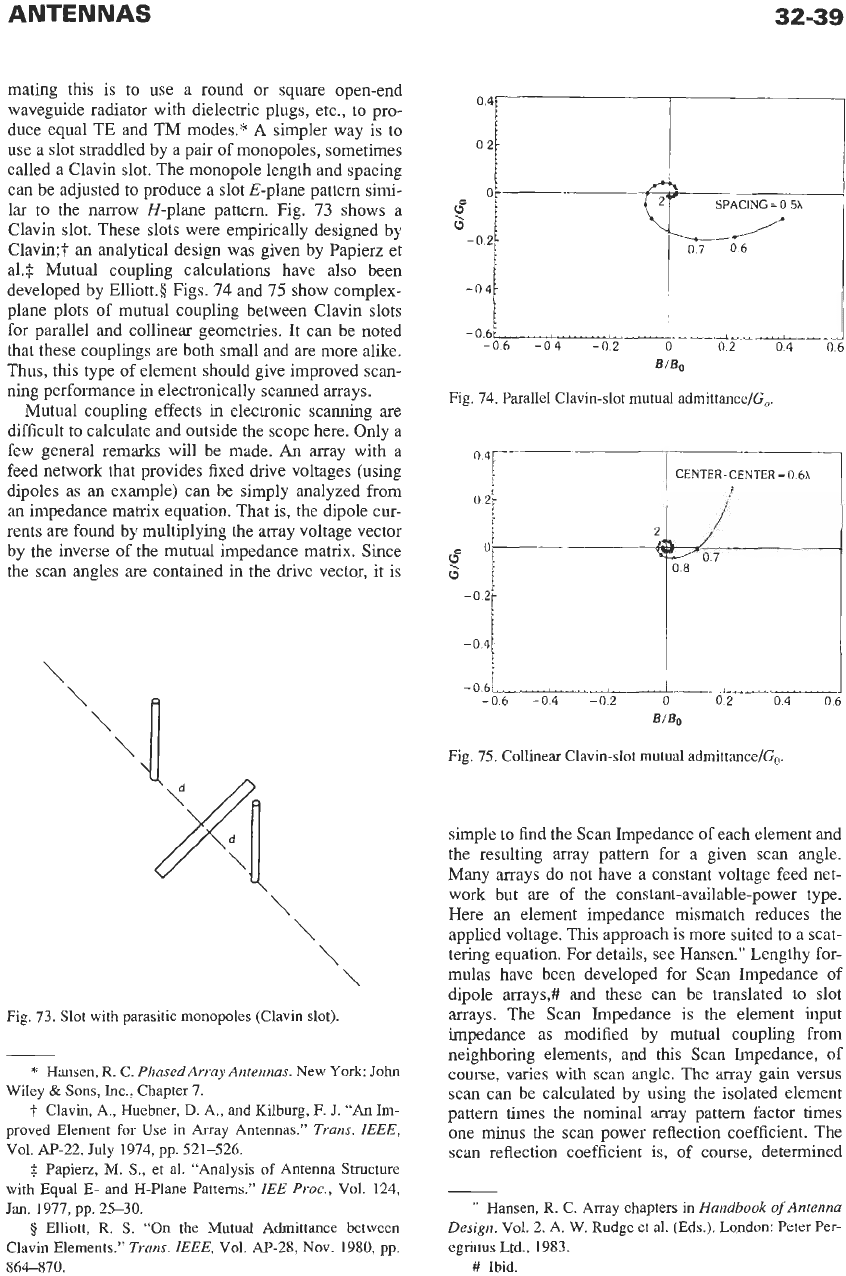
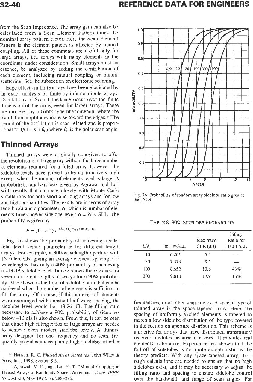
halfwave dipoles. Figs.
70,
71, and
72
show complex-
plane spiral plots of mutual impedance between paral-
0
41
I
I
I
I
I
SPACING
=
0
3X
Fig. 70. Parallel dipole mutual impedance&.
*
Hansen,
R.
C. Array Chapters in
Handbook
of
Antenna
Design.
Vol.
2.
A.
W.
Rudge et al. (Eds.). London: Peter Per-
egrinus Ltd., 1983.
t
Elliott,
R.
S.
Antenna Theory and Design.
Englewood
Cliffs,
NJ
Prentice-Hall, Inc., 1981.
04
-0
6
-06
-04
-02
0
02
04
06
RIRO
Fig. 71.45” echelon dipole mutual impedance&.
O
4k
CENTER-CENTER
-
0
5X
t
-0
6
.,,
,LY
02
04
0
-04i,,
,,,
,,
, ,
,,
(,,
,
,,,
,! ,
-06
-04 -02
0
RIRo
Fig.
72. Collinear dipole mutual impedance&
lel, collinear, and
45”
echelon dipoles. The circles on
the graph represent different values of dipole center-
to-center spacing. It is important to note that the
H-
plane coupling is strong while the E-plane coupling is
weak. Accurate and efficient computer codes in For-
tran for the calculation
of
mutual impedance have been
given by Hansen8 for equal lengths and Hansen and
BrunnerS3 for unequal dipoles. These results and codes
can be used for slots by replacing the dipole with a
Booker equivalent Babinet dipole. The slot admittance
and dipole impedance are related by
2Z,,
=
$Y,,
where
77
=
120~.
If the slot radiates on both sides, the
factor
2
is replaced by
4.
The strong mutual coupling could be reduced if the
element power pattern could be transformed into the
ideal symmetric cos
0 pattern. One way of approxi-
$
Hansen,
R.
C. “Formulation
of
Echelon Dipole Mutual
Impedance for Computer.”
Trans.
IEEE,
Al-20,
Nov.
1972,
pp. 780-781.
0
Hansen, R. C., and Brunner,
G.
“Dipole Mutual Imped-
ance
for
Design of Slot Arrays.”
Microwave
J.,
Vol. 22,
De-
cember 1979, pp.
54-56.
ANTENNAS
32-39
mating this is to use a round or square open-end
waveguide radiator with dielectric plugs, etc., to pro-
duce equal
TE
and TM modes.”
A
simpler way is to
use a slot straddled by a pair of monopoles, sometimes
called a Clavin slot. The monopole length and spacing
can be adjusted
to
produce a slot E-plane pattern simi-
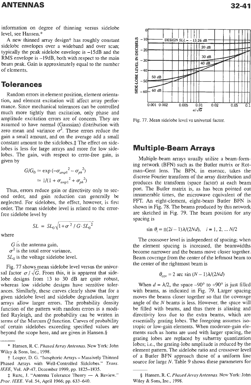
lar to the narrow H-plane pattern. Fig.
73
shows a
Clavin slot. These slots were empirically designed by
Clavin;? an analytical design was given by Papierz et
al.3 Mutual coupling calculations have also been
developed by Elliott.§ Figs.
74
and
75
show complex-
plane plots of mutual coupling between Clavin slots
for parallel and collinear geometries. It can be noted
that these couplings are both small and are more alike.
Thus, this type of element should give improved scan-
ning performance in electronically scanned arrays.
Mutual coupling effects in electronic scanning are
difficult to calculate and outside the scope here. Only a
few general remarks will be made.
An
array with a
feed network that provides fixed drive voltages (using
dipoles as an example) can be simply analyzed from
an impedance matrix equation. That is, the dipole cur-
rents are found by multiplying the array voltage vector
by the inverse of the mutual impedance matrix. Since
the scan angles are contained in the drive vector,
it
is
\
\
\
\
\
Fig. 73. Slot with parasitic monopoles (Clavin slot).
*
Hansen,
R.
C.
PhasedArray Antennas.
New
York: John
Wiley
&
Sons,
Inc., Chapter 7.
t
Clavin,
A.,
Huebner,
D.
A.,
and Kilburg,
F.
J.
“An
Im-
proved Element for
Use
in Array Antennas.”
Trans.
IEEE,
Vol. A€-22, July 1974, pp. 521-526.
Papierz,
M.
S., et
al.
“Analysis
of
Antenna Structure
with
Equal
E-
and H-Plane Patterns.”
ZEE
Puoc.,
Vol. 124,
Jan.
1977, pp. 25-30.
8
Elliott,
R.
S.
“On
the Mutual Admittance between
Clavin Elements.”
Trans.
IEEE,
Vol. AP-28, Nov. 1980, pp.
864-870.
0
0
0,
0
-0 2
-04
-06
-04
-02
0
02
04
06
BIB,
Fig.
74.
Parallel Clavin-slot mutual admittance/G,
1
CENTER-CENTER=O
6h
I
r
I
Fig. 75. Collinear Clavin-slot mutual admittance/Go.
simple to find the Scan Impedance of each element and
the resulting array pattern for a given scan angle.
Many arrays do not have a constant voltage feed net-
work but are of the constant-available-power type.
Here an element impedance mismatch reduces the
applied voltage.
This
approach is more suited to a scat-
tering equation. For details, see Hansen.” Lengthy for-
mulas have been developed for Scan Impedance of
dipole arrays,# and these can be translated
to
slot
mays. The Scan Impedance is the element input
impedance as modified by mutual coupling from
neighboring elements, and this Scan Impedance, of
course,
varies
with
scan
angle.
The
may
gain
versus
scan can be calculated by using the isolated element
pattern times the nominal array pattern factor times
one minus the scan power reflection coefficient. The
scan reflection coefficient
is,
of
course, determined
’’
Hansen,
R.
C. Array chapters in
Handbook
of
Antenna
Design.
Vol. 2.
A.
W. Rudge et al. (Eds.). London: Peter Per-
egrinus Ltd., 1983.
#
Ibid.
32-40
REFERENCE
DATA
FOR ENGINEERS
from the Scan Impedance. The array gain can also be
calculated from a Scan Element Pattern times the
nominal array pattern factor. Here the Scan Element
Pattern
is
the element pattern as affected by mutual
coupling. All of these comments are useful only for
large arrays, i.e., arrays with many elements in the
coordinate under consideration. Small arrays must, in
essence, be analyzed by adding the contribution
of
each element, including mutual coupling or mutual
scattering. See the subsection
on
electronic scanning.
Edge effects in finite arrays have been elucidated by
an exact analysis of finite-by-infinite dipole arrays.
Oscillations in Scan Impedance occur over the finite
dimension of the array, even for larger arrays. These
are
modeled by a Gibbs type phenomenon, where the
oscillation amplitudes increase toward the edges.” The
period of the oscillation is scan related and is propor-
tional to
141
-
sin
6,)
where
6,
is the polar scan angle.
Thinned
Arrays
Thinned arrays were originally conceived
to
offer
the resolution of a large array without the large number
of elements required for a filled array. However, the
sidelobe levels have proved to be unattractively high
except when the number of elements used is large. A
probabilistic analysis was given by Agrawal and
Lot
with results that compare closely with Monte Carlo
simulations for both short and long arrays and for low
and high probabilities. The results are in terms
of
array
length
L/h
and a parameter,
a,
which is number
of
ele-
ments times power sidelobe level:
a
=
N
x
SLL.
The
probability is given by
Fig.
76
shows the probability of achieving a side-
lobe level versus parameter
a
for different length
arrays. For example, a 300-wavelength aperture with
150
elements, giving an average element spacing of
2
wavelengths, has only a
40%
probability of achieving
a -13
dB
sidelobe level. Table
8
shows the
a
values for
several different lengths of arrays for a
90%
probabil-
ity. Also shown is the limit of sidelobe ratio that can be
achieved when the number of elements is sufficient to
fill the array. Of course, if this number of elements
were rearranged with constant half-wave spacing, the
sidelobe level would be
-13.26
dB. The filling ratio
necessary to achieve a
90%
probability of sidelobes
below
-10
dB
is
also shown. From this, it can be seen
that either high filling ratios or large arrays are needed
to
achieve even modest sidelobe levels. A thinned
array designed for one frequency and no scan, fre-
quently provides unacceptably high sidelobes at other
*
Hansen,
R. C.
Phased
Array
Antennas.
John
Wiley
&
Sons, Inc.,
1998,
Section
8.3.
t
Agrawal,
V.
D.,
and
Lo,
Y.
T.
“Mutual
Coupling in
Phased Arrays
of
Randomly Spaced Antennas.”
Trans.
IEEE,
Vol.
AP-20.
May
1972,
pp.
288-295.
NISLR
Fig.
76.
Probability
of
random array sidelobe ratio greater
than SLR.
TABLE
8.90%
SIDELOBE
PROBABILITY
Filling
Maximum Ratio
for
Wh
a
=
N+LL
SLR
(dB)
10
dB
SLL
10
6.201 5.1
-
30 7.373 9.1
-
100
8.652 13.6 43%
300
9.813 17.9 16%
frequencies,
or
at other scan angles. A special
type
of
thinned array is the space-tapered array. Here, the
spacing of uniformly excited elements is tapered to
match a low sidelobe distribution of the type covered
in the section on aperture distribution. This scheme is
attractive for arrays that have distributed transmitter/
receiver modules because it allows all modules and
elements to be alike. Experience has shown that the
fall-off of sidelobes is not quite
as
optimistic as the
theory predicts. With any space-tapered array, thor-
ough calculations are needed to ensure that no high
sidelobes exist, and it may be necessary to adjust the
filling ratio and spacing to ensure sidelobe control
over the bandwidth and range of scan angles. For
ANTENNAS
32-41
information
on
degee of thinning versus sidelobe
level, see Hansen.*
A
new thinned array design? has roughly constant
sidelobe envelopes over a wideband and over scan;
typically the peak sidelobe envelope is -15dB and the
RMS
envelope is -19dB, both with respect
to
the main
beam peak. Gain is approximately equal to the number
of elements.
To
I
era
n
c
es
Random errors in element position, element orienta-
tion, and element excitation will affect array perfor-
mance. Since mechanical tolerances can be controlled
much more tightly than excitation, only phase and
amplitude excitation errors are of concern. They
are
assumed to have normal (Gaussian) distribution with
zero mean and variance
2.
These errors reduce the
gain a small amount, and
on
the average add a small
constant amount
to
the side1obes.S The effect
on
side-
lobes is less for large arrays and more for low side-
lobes. The gain, with respect to error-free gain, is
given by
2
GIG, exp
(-aampl
-
a,;)
=
1/(1
+
aamp12
+
ab;)
Thus, errors reduce gain or directivity only
to
sec-
ond order, and gain reduction can generally be
neglected. For sidelobes, the effect, however, is first
order. The mean sidelobe level is related to the error-
free sidelobe level by
SL
=
SLodl+a2 /G.SLo2
where
G
i’s
the antenna gain,
a2
is the total error variance,
SL,
is the voltage sidelobe level.
Fig. 77 shows mean sidelobe level versus the univer-
sal factor
u
/
&.
From this, it is apparent that side-
lobe designs from
13
to
30
dB are quite robust,
whereas low sidelobe designs have sensitive toler-
ances. Similarly, these curves clearly show that for a
given sidelobe level and sidelobe degradation, larger
arrays allow larger errors. The probability density
function
of
the pattern with random errors is a modi-
fied Rayleigh, and the probability can be written in
terms
of
the
Marcum
Q
function.
Curves
of
probability
of certain sidelobes exceeding specified values are
beyond the scope here, and are given in Hansen.5
*
Hansen,
R. C.
PhasedArray Antennas.
New York: John
Wiley
&
Sons, Inc., 1998.
t
Leeper, D.
G.
“Isosphoric Arrays -Massively Thinned
Phased Arrays with Well-Controlled Sidelobes.”
Trans.
IEEE,
Val.
AF-47,
December 1999, pp. 1825-1835.
$
Ruze,
J.
“Antenna Tolerance Theory
-
A Review.”
Proc. IEEE.
Vol.
54,
April 1966; pp. 633-640.
0
2
-lo
g
-20
1::
B
9
-50
d
8
-60
o/
&
Fig.
77.
Mean sidelobe level vs universal factor.
Multiple-Beam Arrays
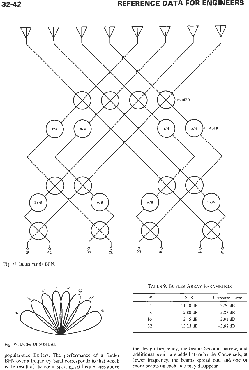
Multiple-beam arrays usually utilize a beam-form-
ing network (BFN) such as the Butler matrix or Rot-
man-Gent lens. The BFN, in essence, takes the
discrete Fourier transform of the array distribution and
produces the transform (space factor) at each beam
port. The Butler matrix is, as has been pointed out
innumerable times, the microwave equivalent of the
FFT.
An
eight-element, eight-beam Butler BFN is
shown in Fig. 78. The beams produced by this network
are sketched in Fig. 79. The beam position for any
spacing is
sin
0,
=
f(2i
-
l)A/(2Ncl),
i
=
1,2,
...
N/2
The crossover level is independent of spacing; when
the element spacing is increased, the beamwidths
become narrower and the beams move closer together.
Beam coverage from the center of the leftmost beam to
the center of the rightmost beam is
e,,,
=
2
arc sin
(N
-
l)A/(2Nd)
When
d
=
A/2,
the space -90” to +90” is just filled
with beams, as indicated in Fig. 79. Larger spacing
moves the beams closer together
so
that the coverage
angle of the
N
beams is less. However, the space will
be filled with beams, and thus there is aliasing and
directivity
loss
due to the extra beams, which are
essentially grating lobes. The foregoing assumes
iso-
tropic or low-gain elements. When moderate-gain ele-
ments such as horns are used with larger spacing, the
grating lobes are replaced by subarray quantization
lobes; Le., the grating-lobe amplitude is reduced by the
element pattern. The sidelobe ratio and crossover level
of
a Butler BFN approach those of a uniform line
source for large
N.
Table 9 shows these parameters for
5
Hansen,
R.
C. PhasedArray Antennas.
New York:
John
Wiley
&
Sons,
Inc., 1998.
32-42
REFERENCE
DATA
FOR ENGINEERS
Fig.
78.
Butler
matrix BFW.
R
4L
TABLE
9.
BUTLER
ARRAY
PARAMETERS
N
SLR
Crossover Level
4
11.30 dB -3.70
dB
8 12.80 dB -3.87
dB
16 13.15 dB -3.91
dB
32 13.23 dB -3.92
dB
Fig.
79.
Butler
BFN
beams.
popular-size Butlers. The performance
of
a Butler
BFN over
a
frequency band corresponds
to
that which
is
the result
of
change
in
spacing. At frequencies above
the design frequency, the beams become narrow, and
additional beams are added at each side. Conversely, at
lower frequency, the beams spread out, and one or
more beams on each side may disappear.
ANTENNAS
32-43
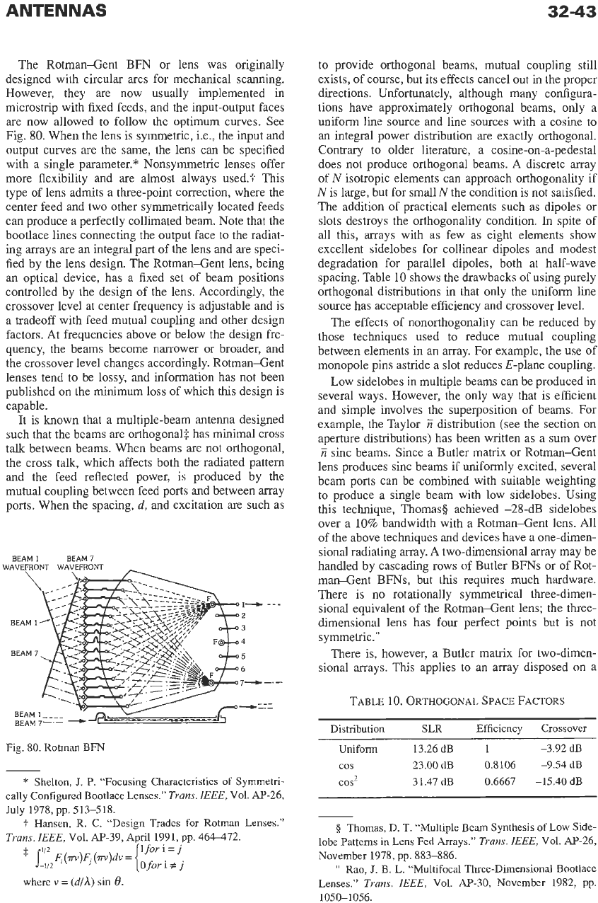
The Rotman-Gent BFN or lens was originally
designed with circular arcs for mechanical scanning.
However, they are now usually implemented in
microstrip with fixed feeds, and the input-output faces
are
now
allowed to follow the optimum curves. See
Fig.
80.
When the lens is symmetric, Le., the input and
output curves
are
the same, the lens can be specified
with a single parameter.* Nonsymmetric lenses offer
more flexibility and are almost always used.? This
type of lens admits a three-point correction, where the
center feed and two other symmetrically located feeds
can produce a perfectly collimated beam. Note that the
bootlace lines connecting the output face to the radiat-
ing arrays are an integral part of the lens and are speci-
fied by the lens design. The Rotman-Gent lens, being
an optical device, has a fixed set of beam positions
controlled by the design of the lens. Accordingly, the
crossover level at center frequency is adjustable and is
a tradeoff with feed mutual coupling and other design
factors. At frequencies above or below the design fre-
quency, the beams become narrower or broader, and
the crossover level changes accordingly. Rotman-Gent
lenses tend to be lossy, and information has not been
published
on
the minimum loss of which
this
design is
capable.
It is known that a multiple-beam antenna designed
such that the beams
are
orthogonal$ has minimal cross
talk between beams. When beams are not orthogonal,
the cross talk, which affects both the radiated pattern
and the feed reflected power, is produced by the
mutual coupling between feed ports and between array
ports. When the spacing,
d,
and excitation are such as
BEAM
1
BEAM7
WAVEFRONT WAVEFRONT
BEAM
7---
Fig.
80.
Rotman
BFN
*
Shelton,
J.
P. “Focusing Characteristics of Symmetri-
cally Configured Bootlace Lenses.”
Trans.
IEEE,
Vol.
AF-26,
July
1978,
pp.
513-518.
t
Hansen,
R. C. “Design Trades for
Rotman
Lenses.”
Truns.
IEEE,
Vol.
A€-39,
April
1991,
pp.
464-472.
where
v
=
(d/h)
sin
8.
to provide orthogonal beams, mutual coupling still
exists, of course, but its effects cancel out in the proper
directions. Unfortunately, although many configura-
tions have approximately orthogonal beams, only a
uniform line source and line sources with a cosine to
an integral power distribution are exactly orthogonal.
Contrary to older literature, a cosine-on-a-pedestal
does not produce orthogonal beams. A discrete array
of
N
isotropic elements can approach orthogonality if
N
is large, but for small
N
the condition is not satisfied.
The addition of practical elements such as dipoles or
slots destroys the orthogonality condition.
In
spite
of
all this, arrays with
as
few as eight elements show
excellent sidelobes for collinear dipoles and modest
degradation for parallel dipoles, both at half-wave
spacing. Table
10
shows
the
drawbacks of using purely
orthogonal distributions in that only the uniform line
source has acceptable efficiency and crossover level.
The effects of nonorthogonality can be reduced by
those techniques used to reduce mutual coupling
between elements in an array. For example, the use of
monopole pins astride a slot reduces E-plane coupling.
Low sidelobes in multiple beams can be produced in
several ways. However, the only way that is efficient
and simple involves the superposition of beams. For
example, the Taylor
Ti
distribution (see the section
on
aperture distributions) has been written as a sum over
Ti
sinc beams. Since a Butler matrix or Rotman-Gent
lens produces sinc beams if uniformly excited, several
beam ports can be combined with suitable weighting
to produce a single beam with low sidelobes. Using
this technique, Thomas5 achieved -28-dB sidelobes
over a
10%
bandwidth with a Rotman-Gent lens. All
of the above techniques and devices have a one-dimen-
sional radiating array. A two-dimensional array may be
handled by cascading rows of Butler BFNs or of Rot-
man-Gent BFNs, but this requires much hardware.
There is
no
rotationally symmetrical three-dimen-
sional equivalent of the Rotman-Gent lens; the three-
dimensional lens has four perfect points but is not
symmetric.”
There is, however, a Butler matrix for two-dimen-
sional arrays. This applies to an array disposed
on
a
TABLE
10.
ORTHOGONAL SPACE FACTORS
Distribution SLR Efficiency Crossover
Uniform
13.26
dB
1
-3.92
dB
cos
23.00
dB
0.8106 -9.54
dB
cos2
31.47
dB
0.6667 -15.40
dB
5
Thomas,
D.
T.
“Multiple Beam Synthesis of Low Side-
lobe Patterns in Lens Fed Arrays.”
Trans.
IEEE,
Vol.
AF-26,
November
1978,
pp.
883-886.
”
Rao,
J.
B.
L.
“Multifocal Three-Dimensional Bootlace
Lenses.”
Trans.
IEEE,
Vol.
AP-30,
November
1982,
pp.
1050-1056.
32-44
REFERENCE
DATA
FOR ENGINEERS
regular hexagonal lattice. The resulting BFN is
a
three-
dimensional microwave network with multiple-ann
hybrid junctions but is simpler than cascading two-
dimensional Butler BF’Ns.”
Electronic Scanning
Some of the design tradeoffs for electronic scan-
ning, such
as
grating lobes, have been addressed
above. A large electronic scanning array, or phased
array, can be characterized in terms of Scan Impedance
and Scan Element Pattern; the modifier “scan” implies
a
quantity that varies with scan angles.
In
the Scan
Impedance approach, the pattern is written
as
the prod-
uct of three factors. First is the array factor (of isotro-
pic elements), which is
h,;
the second is the isolated
element pattern,
g,;
the last term involves the Scan
Impedance. These combine to give
a
gain pattern
of
where
R,
is the isolated element resistance,
R,
is the scan element resistance,
r,
is the scan reflection coefficient.
Scan Impedance can be measured only when
all
ele-
ments are radiating with the proper amplitude and
phase. The Scan Element Pattern can be measured
with
a
distant transmitter and all elements terminated
in
a
matched load. It shows relative behavior versus
scan angles. If one element is excited, relative angle
behavior is useful but the absolute value is not.
Although these formulas show only
8,
they apply in
general to two-dimensional scanning over
8,
4.
For
such large arrays,
a
powerful analysis was developed
by Oliner and colleagues using the unit cell concept.
Here, one element in a large array is seen to be closely
equivalent to an element in an infinite array; in the lat-
ter, the periodic nature
of
the array allows
a
single cell
to contain the entire characteristics of the array. This
cell, called the unit cell, consists of
a
virtual
waveguide with suitably chosen impedance walls with
the waveguide symmetrically located about the ele-
ment (typically
a
slot) in the element lattice. The wall
boundary conditions are derived from the scan angles.
These unit cells are normal to the array face and are
contiguous. Interior modes are
LSE
and/or
LSM.
If no
grating lobes exist, the conductance is given by the
single propagating mode
in
the unit cell waveguide,
and thus
a
closed
form
result occurs. All modes con-
tribute susceptance, and thus many series terms must
*
Williams,
W.
F., and Schroeder.
K.
G. “Performance
Analysis
of
Planar Hybrid Matrix Arrays.”
Trans.
ZEEE,
Val.
A€-27,
July
1969,
pp.
526-528.
McFarland,
J.
L.
“The
RN2
Multiple Beam-Array Family and Beam-Forming Matrix.”
IEEEAPS
Symp.
Digest,
1979,
pp.
728-731.
be computed. This Floquet method has proved to be
powerful and perceptive in the understanding of scan-
ning behavior
of
arrays. For more detailed informa-
tion, refer to Oliner and Malecht and Hansen.$
Applications to arrays of microstrip patches have also
been made.§
A blind spot can be produced in an array at
a
partic-
ular angle; the array radiation is zero at this angle.
This
occurs when the dominant mode is canceled by
a
higher mode, and can occur because of external or
internal structure. External structure often used for
matching or for protective purposes includes dielectric
sheets over or near the array face and dielectric plugs
protruding from waveguide-type elements. Internal
structure includes dielectric loaded waveguide ele-
ments, monopole loaded slots, etc. Blind spots can be
severe for large arrays but usually are negligible for
small arrays. In case
a
blind spot is experienced, the
array design can usually be changed to remove it.
Typ-
ical measures are reducing lattice dimensions, chang-
ing design to improve VSWR, and altering the
periodicity of the external structure. Simulators have
also proved useful. For more detailed information, see
Oliner and Malechj and Hansen.$
Small arrays are usually analyzed with the element-
by-element approach. Here,
a
matrix equation is set up
relating the drive voltage to the element currents times
the impedance matrix, using dipoles
as
an example.
These simultaneous equations are solved for the cur-
rents, from which the impedance of each element is
immediately available. Note that solution of complex
simultaneous equations is several times faster than
matrix inversion. Since the scan direction appears in
the drive vector, Scan Impedance is easily obtained.
This approach allows the variation
of
impedance from
center
to
edge elements to be determined. When the
elements are slots or dipoles,
a
convenient and efficient
computer algorithm for mutual impedance is useful.”
The effects
of
Scan Impedance change over
a
range of
scan angles can be reduced by designing the element
to have
a
pattern close to the “ideal” element pattern.
t
Oliner, A.
A.,
and Malech,
R.
G.
Chapters
3
and
4
in
Microwave Scanning Antennas.
Val.
11.
R.
C. Hansen (Ed.).
New
York: Academic
Press,
Inc.,
1966;
Los
Altos, CA: Pen-
insula
Publ.,
1985.
$
Hansen, R. C. Array chapters in
Handbook
of
Antenna
Design.
Vol.
2.
A.
W. Rudge et
al.
(Eds.). London: Peter Per-
egrinus Ltd.,
1983;
Phased
Array Antennas.
New York John
Wiley
&
Sons, Inc.,
1998.
0
Pozar,
D. M. “General Relations for a Phased Array of
Printed Antennas Derived from Infinite Current Sheets.”
Trans.
IEEE,
Vol.
AF-33,
May
1985,
pp.
498-504.
Lubin,
Y.,
and Hessel, A. “Wide-Band, Wide-Angle Microstrip Stacked-
Patch-Element Phased Arrays.”
Trans.
IEEE,
Val.
AP-39,
”
Hansen, R. C. “Formulation of Echelon Dipole
Mutual
Impedance for Computer.”
Trans. ZEEE,
Val.
AI-20,
Nov.
1972,
pp.
780-781.
Aug.
1991,
pp.
1062-1070.
ANTENNAS
This is
a
power pattern of cos
I9
(for half-wavelength
spacing);
it
is
a
rotationally symmetric cosine pattern.”
Compensation always involves establishing both TE
and TM modes
(to
make the pattern equal in both
planes), and perhaps additional modes for pattern
shape control. This can be done with open-ended
waveguides with appropriately chosen dielectric plugs
and slabs.? A simpler but less effective technique uses
monopoles astride
a
slot, the “Clavin pins.”$
Use of sub-arrays, where two or more elements are
connected to one phaser, produces quantization lobes
(QL) similar
to
those mentioned under Grating Lobes.
These QL occur at the grating lobe angles (for the sub-
array spacing) but are reduced by the sub-array pat-
terns. It has recently been discovered that these sub-
array QL can be partially decollimated by using
a
pseudo-random phase.§ Fig.
80a
shows the suppressed
QL for an array of 2-element sub-arrays and 30-degree
scan. This technique is
most
useful for 2-element (or
2x2) sub-arrays, due to the pattern effects of larger
sub-arrays.
Adaptive Arrays
Adaptive arrays are sometimes used
to
suppress
interfering sources; the array is automatically adjusted
to
provide
a
pattern null in the direction of the inter-
Fig. 80a. Linear array,
100
elements,
50
sub-arrays,
0
=
30”.
*
Wheeler, H. A. “Simple Relations Derived from a
Phased-Array Antenna Made of
an
Infinite Current Sheet.”
Trans.
IEEE,
Vol.
AI-13,
July
1965,
pp.
506-514.
7
Knittel,
G.
H. “Wide-Angle Impedance Matching of
Phased-Array Antennas: A Survey
of
Theory
and Practice.”
In
Oliner, A. A,, and Knittel, G.
H.
(Eds.).
Phased Array Anten-
nus.
Dedham, MA Artech
House,
Inc.,
1972.
$
Elliott, R.
S.
“On
the
Mutual Admittance Between
Clavin Elements.”
Trans. ZEEE,
Vol.
A€-28,
November
1980,
pp.
864-870.
§
Hansen, R. C., and Charlton, G.
C.
“Subarray Quantiza-
tion Lobe Decollimation.”
Trans.
IEEE,
Vol.
A€-47,
August
1999,
pp.
1237-1239.
ferer. The simplest type is the sidelobe canceller in
which an auxiliary element is used with the main
antenna
to
provide
a
single null.
A
feedback loop is
used to adjust the phase and amplitude of the single
element to produce
a
subtraction of the interfering sig-
nal. A more powerful configuration is the adaptive
array in which each element is controlled. There are
three general types of adaptive arrays, which differ in
the reference signal used for driving the control loops
that provide the weights (amplitude and phase) for
each element. The first type uses an externally pro-
vided steering vector that indicates the desired signal
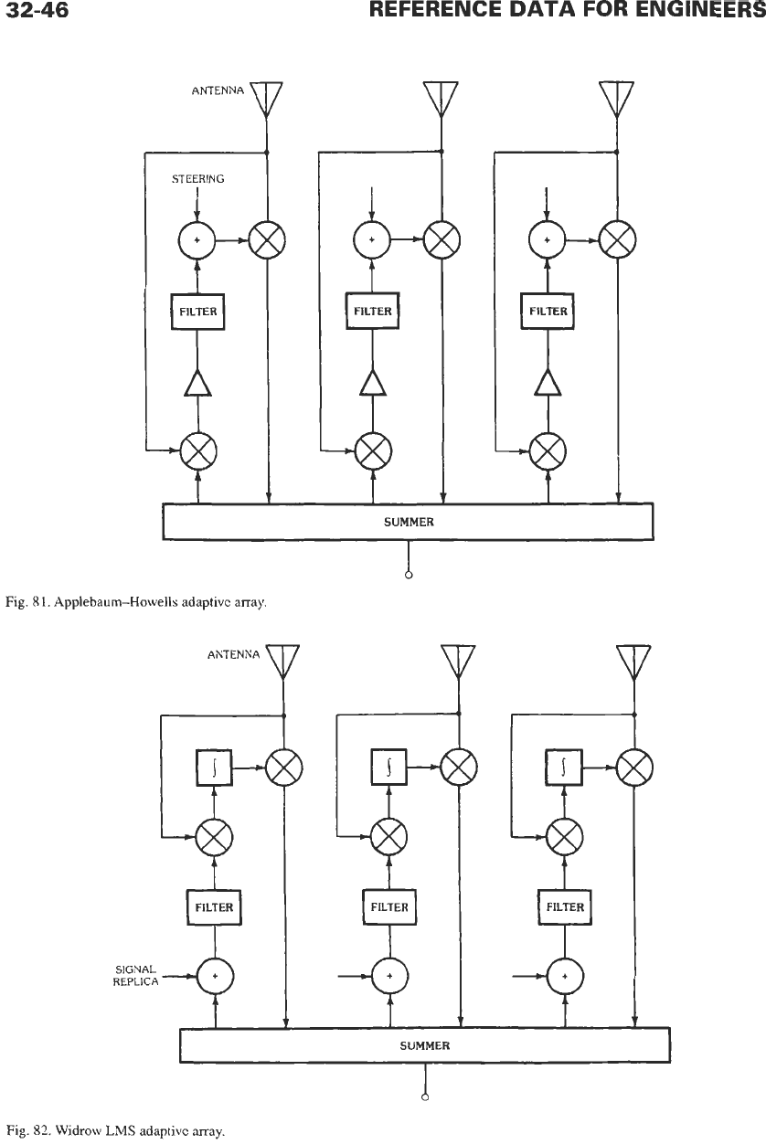
direction. This type of array is called Applebaum-
Howells (Fig.
81);
it is sensitive to errors.” The second
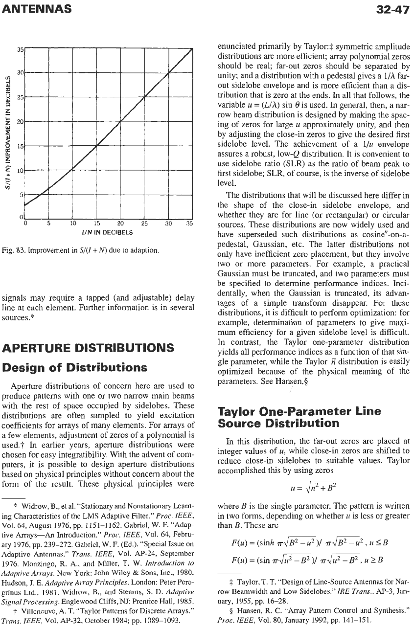
type uses
a
signal replica that correlates with the
desired signal. This replica may be from
a
subcarrier
oscillator,
a
binary sequence of the proper bit rate, etc.
This type of adaptive array is associated with Widrow
and is frequently called an LMS array. Fig. 82 shows
a
simplified configuration. The control loops produce
a
least-mean-square error between the desired signal and
the replica, hence the LMS name. The third type
of
adaptive array does
not
have an externally supplied
reference signal. This array is called
a
power inversion
array and has been associated with Compton. It will
form
a
null
on
the strongest signal with additional
nulls formed
on
weaker signals.
All of these adaptive arrays have
N
-
1
degrees of
freedom, where
N
is the number of elements in one
plane, and
N
-
1
nulls can, in general, be placed in this
plane.
If
there are more degrees of freedom than inter-
ferers, the power inversion array tends to null out the
desired signal as well, since it cannot tell the desired
signal from interfering signals. The improvement
available, essentially independent of the type of adap-
tion, is related to the interference-to-noise ratio. To
illustrate,
a
single interferer is assumed. The ratio
of
signal
to
interference plus noise before and after adap-
tion indicates the improvement (Fig. 83). For large
IiN,
the improvement in
Sl(I
+
N)
is essentially just
IIN,
but
for small values the improvement rapidly decreases.
Convergence depends
on
the ratio of the strongest sig-
nal to the desired signal; strong interferers require
reduced loop gain
to
avoid instability, and this slows
convergence. Methods of accelerating convergence
can utilize orthogonalization of Eigenvalues, or
a
mod-
ified control law. The control loops and weighting can
be performed either with analog or digital hardware.
Thus, there are several configurations possible. Analog
control loops are simple, but some control laws such
as
accelerated convergence are difficult to implement
other than digitally. Adaption in beam space, after
a
beamformer, allows preservation of desired signals
and better rejection control.# Adaptation
of
wideband
’‘
Compton,
R.
T.
Adaptive Antennas.
Englewood Cliffs,
#
Gabriel, W.
F.
“Adaptive Processing Array Systems.”
NJ:
Prentice Hall,
1988.
Puoc.
IEEE,
Vol.
80,
January
1992,
pp.
152-161.
32-46
REFERENCE
DATA
FOR ENGINEERS
ANTENNA
\
SIGN
REPL
$-+
FILTER
4
I
SUMMER
FILTER
T
Fig.
81.
Applebaum-Howells adaptive array.
ANTENNA
I
FILTER
c;]
7
SUMMER
-0
L
A
I
Fig.
82.
Widrow
LMS
adaptive array.
ANTENNAS
32-47
0
5
10
15
20
25
30
35
IIN
IN
DECIBELS
Fig.
83.
Improvement
in
S/(I
+
N)
due
to
adaption.
signals may require a tapped (and adjustable) delay
line at each element. Further information is in several
sources.*
APERTURE DISTRIBUTIONS
Design
of
Distributions
Aperture distributions of concern here are used to
produce patterns with one or two narrow main beams
with the rest of space occupied by sidelobes. These
distributions are often sampled to yield excitation
coefficients for arrays of many elements. For arrays of
a few elements, adjustment
of
zeros of a polynomial is
used.?
In
earlier years, aperture distributions were
chosen for easy integratibility. With the advent of com-
puters, it is possible to design aperture distributions
based
on
physical principles without concern about the
form of the result. These physical principles were
*
Widrow,
B.,
et
al. “Stationary and Nonstationaq
Leam-
ing Characteristics
of
the
LMS Adaptive Filter.”
Proc.
IEEE,
Vol.
64,
August
1976,
pp.
1151-1162.
Gabriel, W.
F.
“Adap-
tive
Arrays-An Introduction.”
Proc.
IEEE,
Vol.
64,
Febru-
ary
1976,
pp.
239-272.
Gabriel,
W.
F.
(Ed.). “Special
Issue
on
Adaptive Antennas.”
Trans.
IEEE,
Vol.
AI-24,
September
1976.
Monzingo,
R.
A,,
and
Miller, T. W.
Introduction to
Adaptive Arrays.
New
York
John
Wiley
&
Sons, Inc.,
1980.
Hudson,
J.
E.
Adaptive Array Principles.
London: Peter
Pere-
grinus
Ltd.,
1981.
Widrow,
B.,
and Steams,
S.
D.
Adaptive
Signal Processing.
Englewood
Cliffs,
NJ Prentice Hall,
1985.
t
Villeneuve,
A.
T.
“Taylor
Patterns
for
Discrete
Arrays.”
Trans.
IEEE,
Vol.
AP-32,
October
1984;
pp.
1089-1093.
enunciated primarily by Taylor:
$
symmetric amplitude
distributions are more efficient; array polynomial zeros
should be real; far-out zeros should be separated by
unity; and a distribution with a pedestal gives a
l/h
far-
out sidelobe envelope and is more efficient than a dis-
tribution that is zero at the ends.
In
all that follows, the
variable
u
=
(Lih)
sin
0
is used. In general, then, a nar-
row beam distribution is designed by making the spac-
ing of zeros for large
u
approximately unity,
and
then
by adjusting the close-in zeros to give the desired first
sidelobe level. The achievement of a
l/u
envelope
assures a robust, 1ow-Q distribution. It is convenient to
use sidelobe ratio
(SLR)
as
the ratio of beam peak to
first sidelobe;
SLR,
of course, is the inverse of sidelobe
level.
The distributions that will be discussed here differ in
the shape of the close-in sidelobe envelope, and
whether they
are
for line (or rectangular) or circular
sources. These distributions are now widely used and
have superseded such distributions as cosine”-on-a-
pedestal, Gaussian, etc. The latter distributions not
only have inefficient zero placement, but they involve
two or more parameters. For example,
a
practical
Gaussian must be truncated, and two parameters must
be specified to determine performance indices. Inci-
dentally, when the Gaussian is truncated, its advan-
tages of a simple transform disappear. For these
distributions, it is difficult to perform optimization: for
example, determination of parameters to give maxi-
mum efficiency for a given sidelobe level is difficult.
In
contrast, the Taylor one-parameter distribution
yields all performance indices as a function of that sin-
gle parameter, while the Taylor
E
distribution is easily
optimized because of the physical meaning of the
parameters. See Hansen.3
Taylor One-Parameter Line
Source Distribution
In
this distribution, the far-out zeros are placed at
integer values of
u,
while close-in zeros are shifted to
reduce close-in sidelobes
to
suitable values. Taylor
accomplished this by using zeros
u
=
7/122+B2
where
B
is the single parameter. The pattern is written
in two forms, depending
on
whether
u
is less or greater
than
B.
These are
F(u)
=
(sinh
mJn)/
mJ-, u
5
B
F(u)
=
(sin
,rrJn)/
mJ=,
u
t
B
$
Taylor, T. T. “Design
of
Line-Source Antennas for Nar-
row Beamwidth and Low
Sidelobes.”
IRE
Trans.,
AI-3,
Jan-
5
Hansen,
R. C.
“Array Pattern Control
and
Synthesis.”
uary,
1955,
pp.
16-28.
Proc.
IEEE,
Vol.
80,
January
1992,
pp.
141-151.