Middleton W.M. (ed.) Reference Data for Engineers: Radio, Electronics, Computer and Communications
Подождите немного. Документ загружается.

32-1
8
REFERENCE
DATA
FOR ENGINEERS
and the cross-polarized radiation also increase, with
undesirable pattern effects. Surface waves may be a
problem for larger arrays or large substrates. An easy
technique to obviate these is
to
make the dielectric
anisotropic, by drilling holes perpendicular to the slab.
Such a slab is sometimes called a Photonic Band Gap
material in analogy to quantum mechanics, but this
nomenclature
is
at best misleading. Most techniques
for extending the bandwidth of patches have done
so
at
the expense of efficiency, i.e., through use of matching
networks with high standing waves. However, the par-
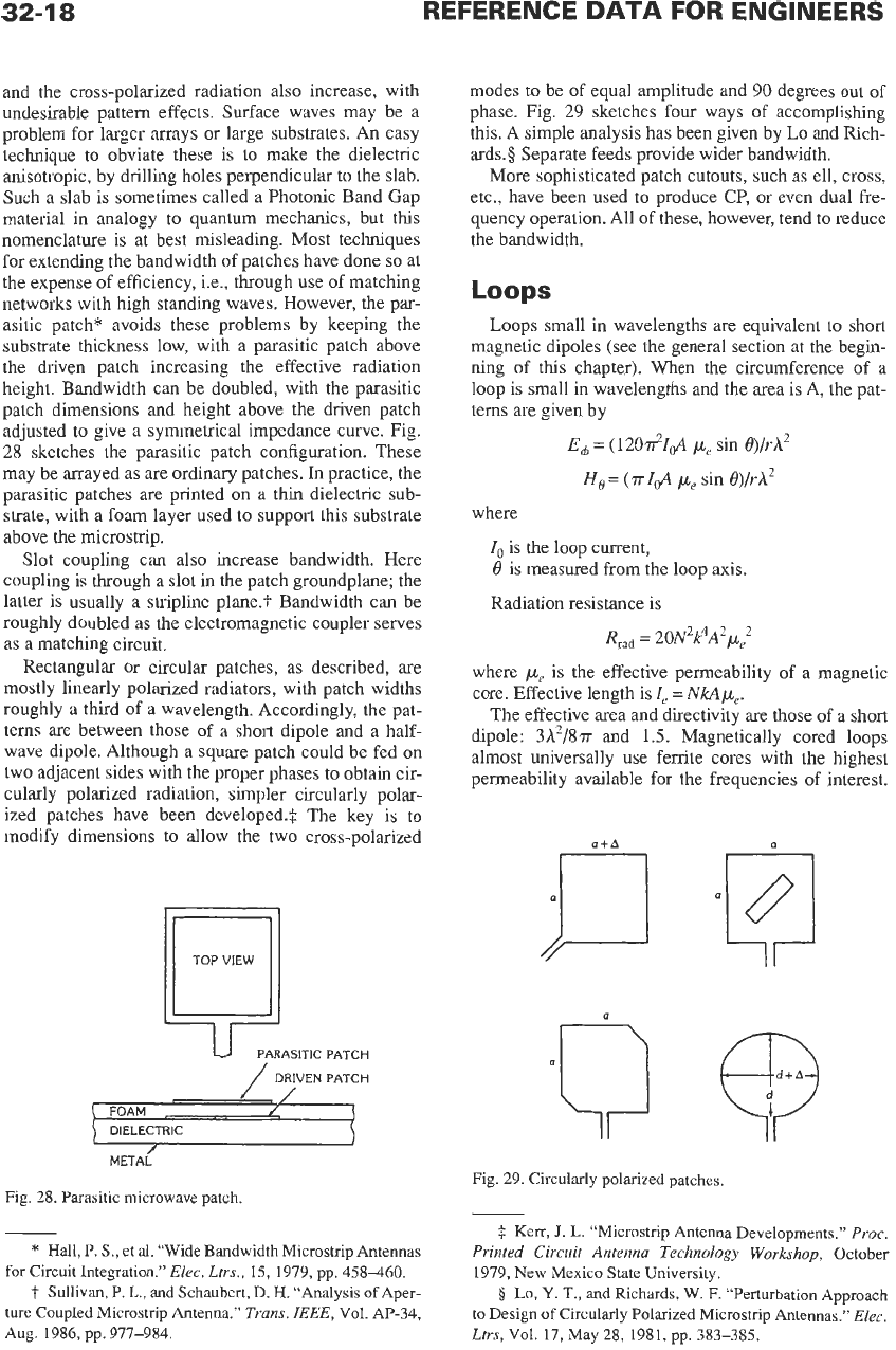
asitic patch* avoids these problems by keeping the
substrate thickness low, with a parasitic patch above
the driven patch increasing the effective radiation
height. Bandwidth can be doubled, with the parasitic
patch dimensions and height above the driven patch
adjusted to give a symmetrical impedance curve. Fig.
28
sketches the parasitic patch configuration. These
may be arrayed as are ordinary patches. In practice, the
parasitic patches are printed on a thin dielectric sub-
strate, with a foam layer used to support this substrate
above the microstrip.
Slot coupling can also increase bandwidth. Here
coupling is through a slot in the patch groundplane; the
latter
is
usually a stripline plane.? Bandwidth can be
roughly doubled as the electromagnetic coupler serves
as a matching circuit.
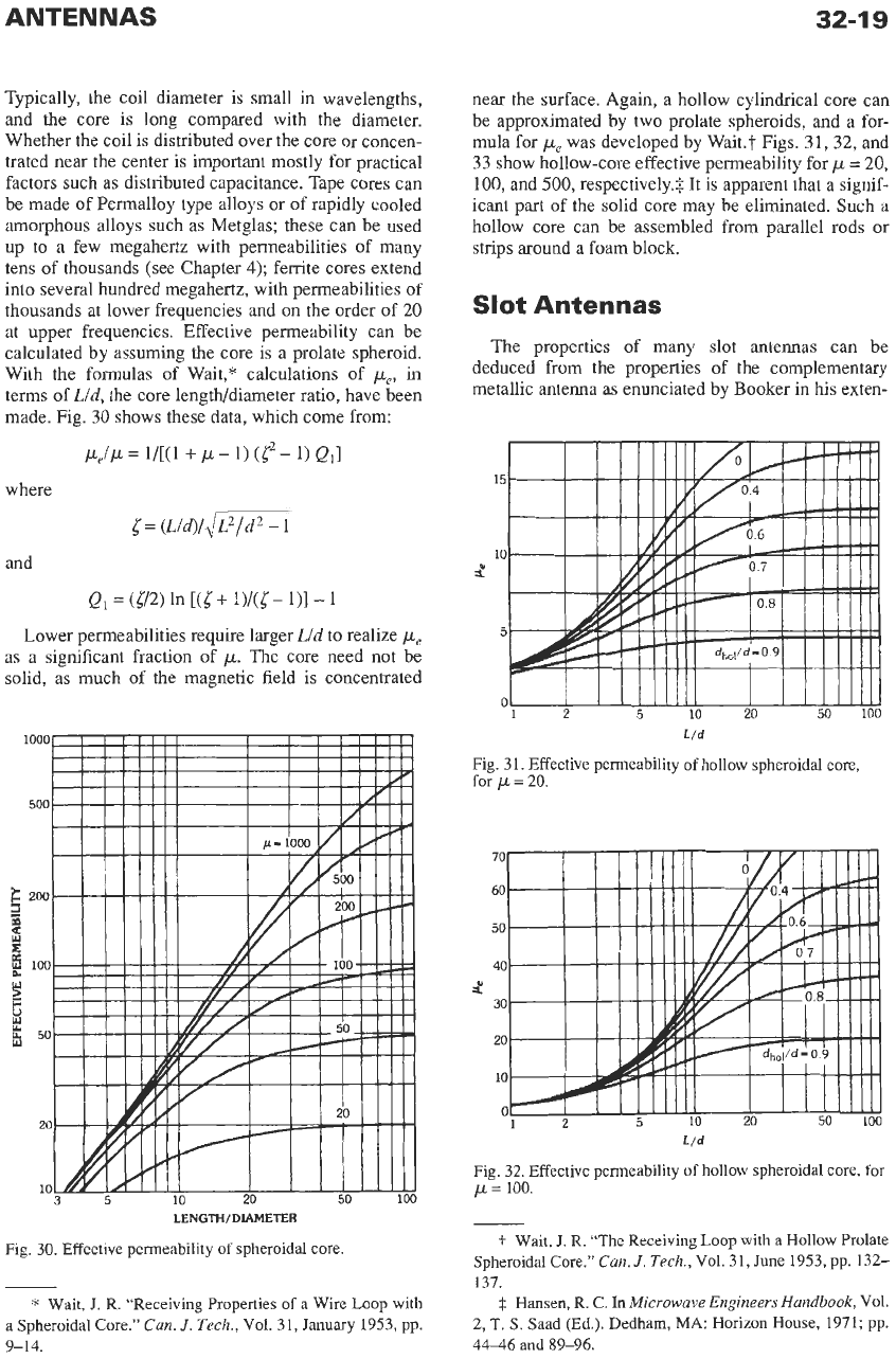
Rectangular or circular patches, as described, are
mostly linearly polarized radiators, with patch widths
roughly a third of a wavelength. Accordingly, the pat-
terns are between those
of
a short dipole and a half-
wave dipole. Although a square patch could be fed on
two adjacent sides with the proper phases to obtain cir-
cularly polarized radiation, simpler circularly polar-
ized patches have been developed.$ The key is to
modify dimensions
to
allow the two cross-polarized
u
,PATCH
DRIVEN
PATCH
/
FOAM
,
/,
DIELECTRIC
modes
to
be of equal amplitude and 90 degrees out of
phase. Fig. 29 sketches four ways of accomplishing
this. A simple analysis has been given by
Lo
and Rich-
ards.
§
Separate feeds provide wider bandwidth.
More sophisticated patch cutouts, such as ell, cross,
etc., have been used to produce CP, or even dual fre-
quency operation. All of these, however, tend to reduce
the bandwidth.
Loops
Loops small in wavelengths are equivalent to short
magnetic dipoles (see the general section at the begin-
ning of this chapter). When the circumference of a
loop is small in wavelengths and the area is A, the pat-
terns are given by
E,
=
(12OdI,,A
p,
sin
O)/uh2
H,
=
(rr
I&
p,
sin
O)/uh2
where
I,
is the loop current,
O
is measured from the loop axis.
Radiation resistance is
Rrad
=
20N2k4A2p:
where
p,
is the effective permeability of a magnetic
core. Effective length is
1,
=
NkAp,.
The effective area and directivity
are
those of a short
dipole:
3h2/8rr
and 1.5. Magnetically cored loops
almost universally use ferrite cores with the highest
permeability available for the frequencies of interest.
f
METAL
Fig. 28. Parasitic microwave patch.
Fig. 29. Circularly polarized patches
*
Hall, P.
S.,
et
al.
“Wide Bandwidth Microstrip Antennas
for Circuit Integration.”
Elec. Ltrs.,
15,
1979, pp. 458460.
t
Sullivan, P.
L.,
and Schaubert, D.
H.
“Analysis of Aper-
ture
Coupled Microstrip Antenna.”
Trans. IEEE,
Vol.
AP-34,
Aug.
1986, pp. 977-984.
$
Kerr,
J.
L.
“Microship Antenna Developments.”
Proc.
Printed Circuit Antenna Technology Workshop,
October
1979,
New
Mexico State University.
5
Lo,
Y.
T.,
and Richards, W.
F.
“Perturbation Approach
to Design of Circularly Polarized Microstrip Antennas.”
Elec.
Ltrs,
Vol.
17, May 28, 1981, pp. 383-385.
ANTENNAS
32-1
9
Typically, the coil diameter is small in wavelengths,
and the core is long compared with the diameter.
Whether the coil is distributed over the core or concen-
trated near the center is important mostly for practical
factors such as distributed capacitance. Tape cores can
be made of Permalloy type alloys or of rapidly cooled
amorphous alloys such as Metglas; these can be used
up
to
a few megahertz with permeabilities of many
tens
of
thousands (see Chapter
4);
ferrite cores extend
into several hundred megahertz, with permeabilities
of
thousands at lower frequencies and
on
the order of
20
at upper frequencies. Effective permeability can be
calculated by assuming the core is a prolate spheroid.
With the formulas
of
Wait,” calculations of
pe,
in
terms
of
Lid,
the core length/diameter ratio, have been
made. Fig.
30
shows these data, which come from:
where
and
Lower permeabilities require larger
Lid
to realize
pe
as a significant fraction of
p.
The core need not be
solid, as much of the magnetic field is concentrated
near the surface. Again, a hollow cylindrical core can
be approximated by two prolate spheroids, and a for-
mula for
pe
was developed by Wait.t Figs.
31, 32,
and
33
show hollow-core effective permeability for
p
=
20,
100,
and
500,
respectively.$ It is apparent that a signif-
icant part of the solid core may be eliminated. Such a
hollow core can be assembled from parallel rods or
strips around a foam block.
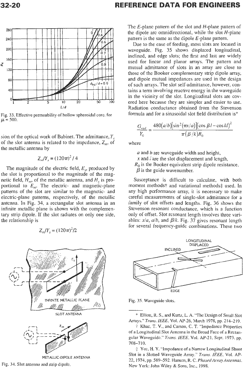
Slot Antennas
The properties of many slot antennas can be
deduced from the properties of the complementary
metallic antenna as enunciated by Booker in
his
exten-
Lld
Fig. 31. Effective permeability
of
hollow spheroidal core,
for
p
=
20.
LENGTH/DIAMETER
t
Wait,
J.
R.
“The Receiving Loop with
a
Hollow Prolate
Spheroidal Core.”
Can.
J.
Tech.,
Vol.
31,
June
1953, pp. 132-
137.
$
Hansen, R. C. In
Microwave Engineers Handbook,
Vol.
2,
T.
S.
Saad (Ed.). Dedham,
MA:
Horizon
House,
1971; pp.
Fig. 30. Effective permeability
of
spheroidal core.
*
Wait,
J.
R.
“Receiving Properties of a Wire Loop with
a
Spheroidal Core.”
Can.
J.
Tech.,
Vol.
31, January 1953, pp.
9-14. 44-46 and 89-96.
32-20
REFERENCE
DATA
FOR
ENGINEERS
Lld
Fig.
33.
Effective permeability of hollow spheroidal core, for
p
=
500.
sion of the optical work of Babinet. The admittance,
Y,
of
the slot antenna is related to the impedance, Z,, of
the metallic antenna by
Zm/Ys=(120~)2/4
The magnitude of the electric field, E,, produced by
the slot is proportional to the magnitude of the mag-
netic field,
H,,,,
of the metallic antenna, and
H,
is pro-
portional to
E,.
The electric- and magnetic-plane
patterns
of
the slot are similar to the magnetic- and
electric-plane patterns, respectively,
of
the metallic
antenna.
In
Fig.
34,
a rectangular slot antenna in an
infinite metallic plane is shown with the complemen-
tary
strip dipole.
If
the slot radiates
on
only one side,
the relationship is
ZJYS
=
(120?r)2/2
/y
INFINITE METALLIC PLANE
h,
SLOT
ANTENNA
METALLIC-DIPOLE ANTENNA
Fig.
34.
Slot antenna and
strip
dipole.
The E-plane pattern of the slot and H-plane pattern of
the dipole are omnidirectional, while the slot H-plane
pattern is the same as the dipole E-plane pattern.
Due to the ease of feeding, most slots are located in
waveguide. Fig.
35
shows displaced longitudinal,
inclined, and edge slots; the first and last are widely
used for linear and planar arrays. The pattern and
mutual admittance of slots in an array are close to
those
of
the Booker complementary strip dipole array,
and dipole mutual impedances are used in the design
of
such arrays. The slot self-admittance, however, con-
tains a term involving reactive energy in the waveguide
in the vicinity of the slot. Longitudinal slots are cov-
ered here because they are simpler and easier
to
use.
Radiation conductance obtained from the Stevenson
formula and for a sinusoidal slot field distribution is*
where
a
and b are waveguide width and height,
x
and
I
are the slot displacement and length,
/3
is the guide wavenumber.
R,
is the Booker equivalent strip dipole resistance,
Susceptance is difficult to calculate, with both
moment methodst and variational methods$ used.
In
any high performance array, it is necessary
to
make
careful measurements of single-slot admittance for a
family of slot offsets and lengths. Fig.
36
shows the
Stevenson resonant conductance, which
is
a function
only of offset. Slot resonant length involves three vari-
ables:
xia,
alb, and
Pik.
Fig.
37
gives resonant length
for several frequency-guide combinations. These two
LONGITUDINAL
Fig.
35.
Waveguide slots.
*
Elliott,
R.
S., and
Kurtz,
L.
A.
“The
Design
of
Small Slot
Arrays.”
Trans.
IEEE,
Vol.
A€-26,
March
1978,
pp.
214-219.
f
Khac,
T.
V., and Carson,
C.
T.
“Impedance Properties
of
a Longitudinal Slot Antenna
in
the
Broad Face
of
a
Rectan-
gular Waveguide.”
Trans.
IEEE,
Vol.
m-21,
Sept.
1973,
pp.
$
Yee,
H.
Y. “Impedance
of
aNarrow Longitudinal Shunt
Slot in a Slotted Waveguide Array.”
Trans.
IEEE,
Vol.
AE-
22,1974,
pp.
589-592.
Hansen,
R.
C.
PhasedAl-ray Antennas.
New York
John
Wiley
&
Sons,
Inc.,
1998.
708-710.
ANTENNAS
32-2
1
10
05
02
01
t”
0‘
0 05
0 02
0
01
0
005
0
005
0
10
0
15
020
025
xla
Fig.
36. Resonant conductance of longitudinal
slot.
was originally thought
to
be a single symmetric curve
for
G/Yo
and a single asymmetric curve for
B/Yo.
As
Fig.
38
shows, it now appears that although all longitu-
dinal slots fit these curves approximately, there are dif-
ferences that vary with
xla,
alb,
and
Plk.
The precise
control of aperture distribution allowed by waveguide
slots and the use
of
computer design have allowed
high-performance low-sidelobe or tailored-sidelobe
arrays to be c0nstructed.t
Slots are sometimes used on cylinders, in either an
axial or circumferential configuration. A circumferen-
tial half-wave slot has a smooth pattern, with the cylin-
der reducing the back lobes. Axial half-wave slots also
exhibit shadowing, with pattern ripples around
4
=
T.
As
ka
increases, the number of ripples increases, but
their depth and angular extent decrease. For both types
of slots, larger cylinders give more shadowing and
lower field at
4
=
T.
Fig.
39
shows typical axial and
circumferential slot patterns in the azimuth plane for
ka
=
8.
These were calculated with the formulas of
Wait:$
Axial
Circumferential
1.4
1.2
1
.o
0.8
0.6
’
0.4
0.2
0
0.6
0.4
0.2
co
$
-0.2
-
0.4
-
0.6
0.90 0.94 0.98
1.02
1.06
1.10
Ill.
Fig.
38. Longitudinal slot admittance,
a
=
0.9,
b
=
0.4,
fre-
quency
=
9375 MHz.
*
Blass, J. “Slot Antennas.” Chapter 8
of
Antenna Engi-
neering Handbook.
R.
C.
Johnson and H. Jasik (Eds.). New
parameters, resonant length and conductance,
are
York: McGraw Hill Book
Co.,
1984.
important because they allow slot admittances versus
frequency to be plotted in the Kaminow and Stegen
“universal” form.* Slot length is given in terms of res-
onant length, and both conductance and susceptance
are given in terms of resonant conductance. The result
t
Elliott,
R.
S.
Antenna
Theory
and Design.
Englewood
Cliffs, NJ: Prentice-Hall, Inc., 1981. Hansen, R. C.
Phased
Array Antennas.
New York: John Wiley
&
Sons,
Inc.,
1998.
$
Wait,
J.
R.
Electromagnetic Radiation from Cylindrical
Structures.
Elmsford, NY: Pergamon Press, Inc., 1959.
32-22
REFERENCE
DATA
FOR ENGINEERS
AZlMUTH
ANGLE
IN
DEGREES
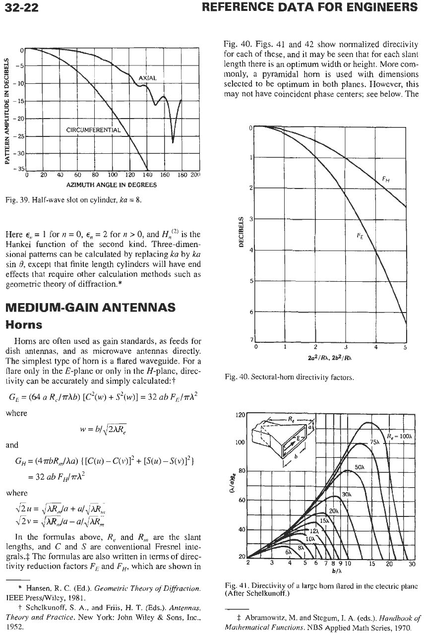
Fig. 39. Half-wave
slot
on cylinder,
ka
=
8.
Here
E,
=
1
for
n
=
0,
E,
=
2
for
n
>
0,
and
H,(2)
is the
Hankel function of the second kind. Three-dimen-
sional patterns can be calculated by replacing
ka
by
ka
sin
8,
except that finite length cylinders will have end
effects that require other calculation methods such as
geometric theory of diffraction.*
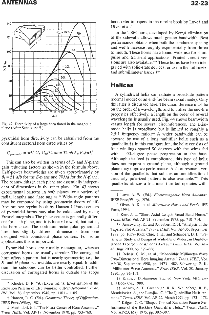
MEDIUM-GAIN ANTENNAS
Horns
Horns
are
often used as gain standards, as feeds for
dish antennas, and as microwave antennas directly.
The simplest type of horn is a flared waveguide. For a
flare only in the E-plane or only in the H-plane, direc-
tivity can be accurately and simply calculated:?
GE
=
(64
a
R,/.rrhb)
[C2(w)
+
S2(w)]
= 32
ab
FE/rA2
where
w
=
b/.J2hRp
and
GH
=
(4.rrbRJAa)
{
[C(u)
-
C(v)I2
+
[S(u)
-
S(V)]~]
=
32 ab
FH/n-A2
where
fiu
=
JQ)a
+
a/&
&v
=
IlhR,Ja
-
a/&
In the formulas above,
Re
and
R,
are the slant
lengths, and
C
and
S
are
conventional Fresnel inte-
grals.$ The formulas are also written
in
terms of direc-
tivity reduction factors
FE
and
FH,
which are shown in
*
Hansen,
R.
C.
(Ed.).
Geometric Theory
of
Diffraction.
IEEE Press/Wiley, 198
1.
t
Schekunoff, S. A.,
and
Friis,
H.
T.
(Eds.).
Antennas,
Theory and Practice.
New York John Wiley
&
Sons,
Inc.,
1952.
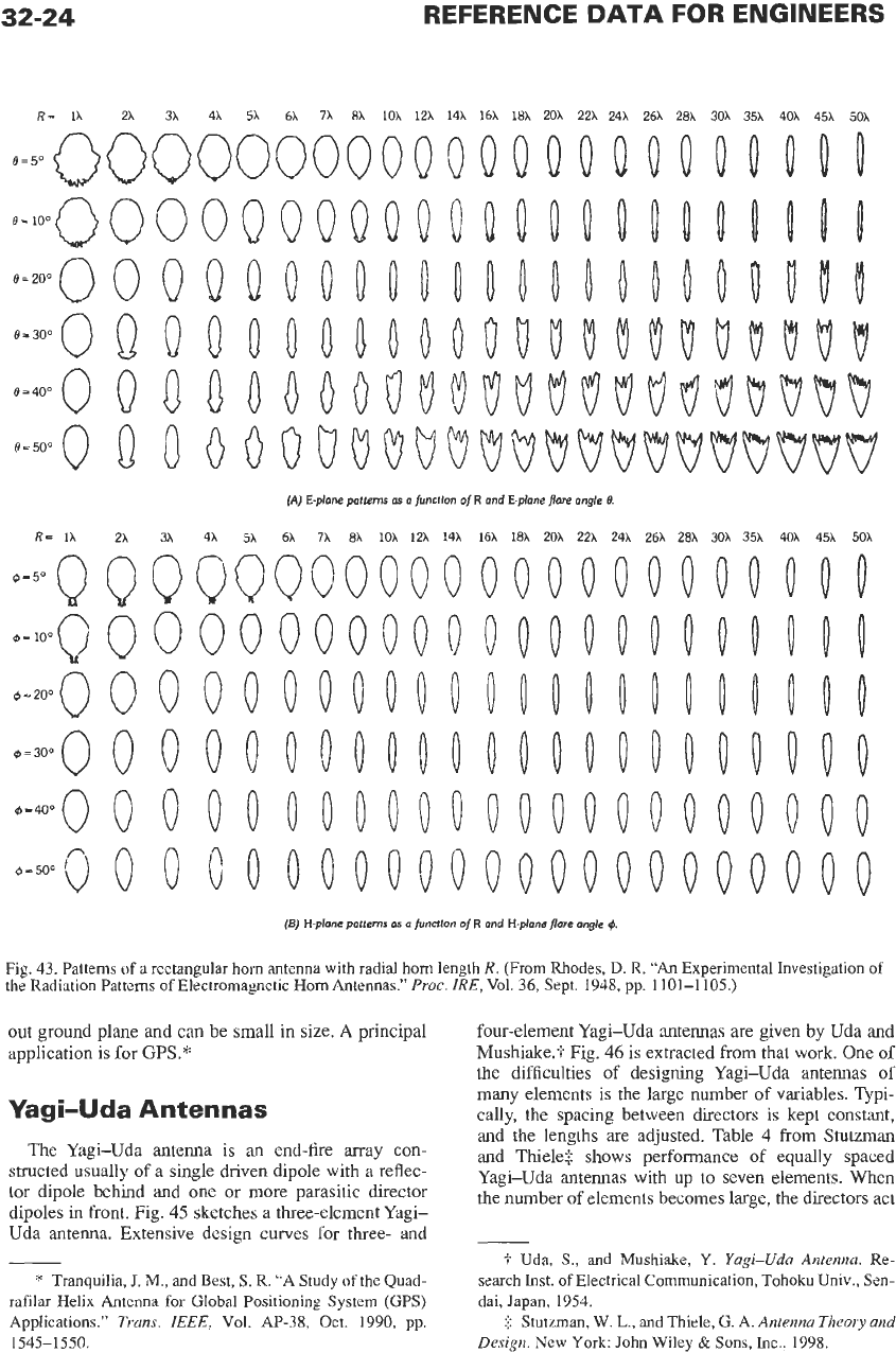
Fig.
40.
Figs.
41
and
42
show normalized directivity
for each of these, and it may be seen that for each slant
length there is an
optimum
width or height. More com-
monly, a pyramidal horn is used with dimensions
selected to be optimum in both planes. However,
this
may not have coincident phase centers; see below. The
0'
y
1
2
23
rp
U
4.
x
5
6-
7.
0
1
4
5
2021RX.
2bZIRh
Fig. 40. Sectoral-horn directivity factors.
b/X
Fig. 41. Directivity of
a
large horn
flared
in
the electric plane
(After Schelkunoff.)
$
Abramowitz,
M.
and
Stegum,
I.
A.
(eds.).
Handbook
of
Mathematical Functions. NBS
Applied
Math
Series, 1970.
ANTENNAS
32-23
here; refer to papers in the reprint book by Love5 and
Olver et al.”
In
the TEM horn, developed by Ken-,# elimination
of the sidewalls allows much greater bandwidth. Best
performance obtains when both the conductor spacing
and width increase roughly exponentially from throat
to mouth. These horns have found wide use for short-
pulse and transient applications. Printed circuit ver-
sions are also available.** These horns have been inte-
grated with solid-state devices for use in the millimeter
and submillimeter bands.tt
o/A
Fig.
42.
Directivity
of
a large horn flared in the magnetic
plane (After Schelkunoff.)
pyramidal horn directivity can be calculated from the
constituent sectoral horn directivities by
Gpyramidd
=
,rrh2
GE
GH/32
ab
=
32
ab
FE
FHf.rrh2
This can also be written in terms of E- and H-plane
gain reduction factors
as
shown in the formula above.
Half-power beamwidths are given approximately by
0,
=
51
h/b
for the E-plane and
7Ohla
for the H-plane.
The beamwidths in each plane are essentially indepen-
dent of dimensions
in
the other plane. Fig.
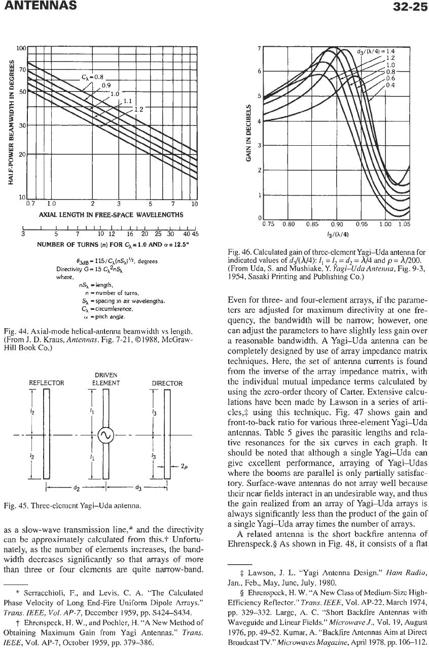
43
shows
experimental patterns in both planes for a variety of
radial lengths and flare angles.* Wide-angle patterns
may be computed by using geometric theory of dif-
fraction; see reprint book by Hansen.? Phase centers
of pyramidal horns may also be calculated by using
Fresnel integrals.$ The phase center is generally differ-
ent for each plane, and it is located toward, but not at,
the horn apex. The optimum rectangular pyramidal
horn has slightly different dimensions from one
designed with coincident phase centers. For some
applications this is important.
Pyramidal horns are usually rectangular, whereas
corrugated horns are usually circular. The corrugated
horn offers
a
pattern that is nearly symmetric; i.e., the
E-
and H-plane beamwidths
are nearly equal.
In
addi-
tion, the sidelobes can be better controlled. Further
discussion of corrugated
horns
is outside the scope
*
Rhodes,
D.
R. “An Experimental Investigation of the
Radiation Patterns of Electromagnetic Horn Antennas.”
Proc.
IRE,
Vol.
36,
September
1948,
pp.
1101
-
1105.
t
Hansen,
R.
C. (Ed.).
Geometric Theoly
of
Diffraction.
IEEE
PressNiley,
1981.
$
Muehldorf,
E.
I.
“The
Phase Center
of
Horn Antennas.”
Trans.
IEEE,
Vol.
AP-18,
November
1970,
pp.
753-760.
Helices
A
cylindrical helix can radiate a broadside pattern
(normal mode) or an end-fire beam (axial mode). Only
the latter is discussed here. The circumference must be
on
the order of a wavelength, and to utilize the end-fire
properties effectively, a length
on
the order of several
wavelengths
is
usually used. Fig.
44
shows beamwidth
versus length for several circumferences. The axial-
mode helix is broadband but is limited to roughly a
2.5:l frequency ratio.$$
A
wider bandwidth can be
covered by use of a long multifilar helix such
as
a
quadhelix.§§
In
this
configuration, the helix consists of
four windings spaced 90 degrees with the wires fed
with
a
90-degree phase progression
at
the base.
Although the feed is complicated, this type of helix
does not require a ground plane, although
a
ground
plane may improve performance.
A
short resonant ver-
sion of the quadhelix that radiates an omnidirectional
circularly polarized pattern is also available.”” This
quadhelix utilizes
a
fractional
turn
but operates with-
§
Love, A. W. (Ed.).
Electromagnetic Horn Antennas.
IEEE
PressNiley,
1976.
Olver, A. D., et
al.
Microwave Horns and Feeds.
IEE
Press,
1994.
#
Ken,
J.
L.
“Short Axial Length Broad-Band Horns.“
Trans.
IEEE,
Vol.
AP-21,
September
1973,
pp.
710-714.
**
Janaswamy,
R.,
and Schaubert, D. H. “Analysis of the
Tapered Slot Antenna.”
Trans.
IEEE,
Vol.
AP-35,
September
1987,
pp.
1058-1065;
Chio,
T.
H., and Schaubert,
D.
H. “Pa-
rameter Study and Design of Wide-Band Widescan Dual-Po-
larized Tapered Slot Antenna Arrays.”
Trans.
IEEE,
Vol
AP-
48,
June
2000,
pp.
879-886.
tt
Rebeiz,
G.
M.,
et.
al., “Monolithic Millimeter-Wave
Two-Dimensional Horn Imaging Arrays.”
Trans.
IEEE,
Vol.
AP-38,
September
1990,
pp.
1473-1482.
Schwering, F.
K.
“Millimeter Wave Antennas.”
Proc.
IEEE,
Vol.
80,
January
1992,
pp.
92-102.
$I
Kraus,
J.
D.
Antennas.
2nd. ed. New York: McGraw-
Hill
Book
Co.,
1988.
§§
Adams, A.
T.,
Greenough,
R.
K.,
Wallenberg, R.
F.,
Mendelovicz, A,, and Lumjiak, C. “The Quadrifilar Helix
At-
tenna.”
Trans.
IEEE,
Vol.
AP-22,
March
1974,
pp.
173
-
178.
””
Kilgus, C. C. “Shaped-Conical Radiation Pattern Per-
formance of
the
Backfire Quadrifilar Helix.”
Truns.
IEEE,
Vol.
AP-23,
May
1975,
pp.
392-397.
32-24
REFERENCE
DATA
FOR ENGINEERS
R=
IX
2X
3X
4h
5X
6X
7X
8X
1OX
1ZX
14X
16X
18X
2OX
22X
24X
26X
28X
30.4
35X
40X
45h
50X
(A)
E-plane patterns
os
a
functlon
of
R
and E-plane
pare
angle
E.
R=
1X
2X
3X
4X
5h
6X
7h
8X
1OX
12X
14X
16X
18X
2OX
22X
24X
26X
28X
30X
35h
40X
45X
50h
4-4)
0
0
0
0
0
0
0
0
0
c
B
0
0
0
0
0
0
0
0
0
0
0
m-300
0
0
0
0
0
0
0
0
0
0
0
0
0
0
0
0
0
0 0
0
0
0
+400OG
0
00
000000000000000000
+=50‘00
0
00000000000000000000
(B)
H-plane patterns
as
a
functlon
of
R
end H.pbne
jlare
angle
4.
Fig. 43. Patterns of a rectangular horn antenna with radial horn length
R.
(From Rhodes,
D.
R.
“An
Experimental Investigation of
the
Radiation Patterns
of
Electromagnetic
Horn
Antennas.”
Proc.
IRE,
Vol.
36,
Sept. 1948, pp. 1101-1105.)
out ground plane and can be small in size.
A
principal
application is for
GPS.”
Yagi-Uda Antennas
The Yagi-Uda antenna is
an
end-fire array con-
structed usually
of
a single driven dipole with
a
reflec-
tor dipole behind and one
or
more parasitic director
dipoles
in
front. Fig.
45
sketches a three-element Yagi-
Uda antenna. Extensive design curves for three- and
*
Tranquilia,
J.
M.,
and Best,
S.
R.
“A Study
of
the Quad-
rafilar Helix Antenna for Global Positioning System
(GPS)
Applications.”
Trans.
ZEEE,
Vol. AP-38, Oct. 1990, pp.
1545-1550.
four-element Yagi-Uda antennas are given by Uda and
Mushiake.? Fig.
46
is extracted
from
that work. One of
the difficulties of designing Yagi-Uda antennas of
many elements is the large number
of
variables. Typi-
cally, the spacing between directors is kept constant,
and the lengths are adjusted. Table
4
from
Stutzman
and Thiele3 shows performance of equally spaced
Yagi-Uda antennas with up to seven elements. When
the number
of
elements becomes large, the directors act
t
Uda,
S.,
and Mushiake,
Y.
Yagi-Uda Antenna.
Re-
search Inst. of Electrical Communication,
Tohoku
Univ., Sen-
dai, Japan, 1954.
$
Stutzman, W.
L.,
and Thiele,
G.
A.
Antenna Theory and
Design.
New
York:
John
Wiley
&
Sons, Inc., 1998.
ANTENNAS
32-25
1W
v)
a
70
E
0
W
50
E
F
3
E
30
m
8
20
10
i!
0.7
1.0
2
3
5
7
10
AXlAL
LENGTH IN FREE-SPACE WAVELENGTHS
I
I
I
IIIII
IIIII
I
Ill1
3
5
7
10
12
16
20
25
30
4045
NUMBER OF TURNS
(n)
FOR
C,=
1.0
AND
a=
12.5O
BQ~B=
115/C,(nS,)”z.
degrees
Directivity
G-
15
C,ZnS,
where,
nSh
-length.
n
-number
of
turns,
Si
-spacing
in
air
wavelengths.
C,
=circumference.
u
=pitch angle.
Fig. 44. Axial-mode helical-antenna beamwidth vs length.
(From
J.
D. Kraus,
Antennas.
Fig. 7-21,01988, McGraw-
Hill Book
Co.)
DRIVEN
REFLECTOR ELEMENT DIRECTOR
T
7
dz
-1-
d3
-
Fig. 45. Three-element Yagi-Uda antenna.
as a slow-wave transmission line,* and the directivity
can
be
approximately
calculated
from
this.?
Unfortu-
nately, as the number of elements increases, the band-
width decreases significantly
so
that arrays of more
than three or four elements are quite narrow-band.
*
Serracchioli, F., and Levis, C.
A.
“The Calculated
Phase Velocity of Long End-Fire Uniform Dipole Arrays.”
Trans.
IEEE,
Vol.
AP-7,
December 1959, pp. S4244434.
t
Ehrenspeck, H.
W.,
and Poehler, H. “A New Method of
Obtaining Maximum Gain from Yagi Antennas.”
Trans.
IEEE,
Vol. AP-7, October 1959, pp. 379-386.
075
080
085
090
095
100
1[
13/(A/4)
Fig.
46.
Calculated gain of
three-element Yagi-Uda
antenna for
indicated values of
d,l(h/4):
I,
=
l2
=
d2
=
h/4 and
p
=
h1200.
(From Uda,
S.
and Mushiake,Y.
Yagi-Uda Antenna,
Fig. 9-3,
1954, Sasaki Printing and Publishing Co.)
Even for three- and four-element arrays, if the parame-
ters are adjusted for maximum directivity at one fre-
quency, the bandwidth will be narrow; however, one
can adjust the parameters to have slightly less gain over
a reasonable bandwidth.
A Yagi-Uda antenna can be
completely designed by use of array impedance matrix
techniques. Here, the set of antenna currents is found
from the inverse of the array impedance matrix, with
the individual mutual impedance terms calculated by
using the zero-order theory of Carter. Extensive calcu-
lations have been made by Lawson in a series of arti-
cles,$ using this technique. Fig.
47
shows gain and
front-to-back ratio for
various
three-element Yagi-Uda
antennas. Table
5
gives the parasitic lengths and rela-
tive resonances for the six curves in each graph. It
should be noted that although a single Yagi-Uda can
give excellent performance, arraying of Yagi-Udas
where the booms are parallel is only partially satisfac-
tory. Surface-wave antennas do not array well because
their near fields interact in an undesirable way, and thus
the gain realized from an array of Yagi-Uda arrays is
always significantly less than the product of the gain of
a single Yagi-Uda array times the number of arrays.
A
related
antenna
is
the short
backfire
antenna
of
Ehrenspeck.5
As
shown
in
Fig.
48,
it consists of a flat
$
Lawson,
J.
L.
“Yagi Antenna Design.”
Ham Radio,
Jan., Feb., May,
June,
July,
1980.
5
Ehrenspeck,
H.
W.
“A New Class of Medium-Size High-
Efficiency Reflector.”
Trans.
IEEE,
Vol. A€-22, March 1974,
pp. 329-332. Large, A. C. “Short Backfire Antennas with
Waveguide and Linear Fields.”
Microwave
J.,
Vol.
19, August
1976, pp. 49-52. Kumar,
A.
“Backfire Antennas
Aim
at Direct
Broadcast
TV.”Microwaves Magazine,
Apnll978, pp. 1061 12.
TBLE
4.
CHARACTERISTICS
OF
EQUALLY SPACED YAGI-UDA ANTENNAS*
I€-Plane E-Plane
N,
~
.-
Front- Input
~.
~
Element Lengths
No.
of
Spacing
Reflector,
L,
Driver,
L
Directors,
L,
Gain to-Back
Impedance
HP,
SLL,
HPE
SLL,
Elements (wavelengths)
(Wavelengths) (wavelengths) (wavelengths) (dB) Ratio(dB)
(ohms)
(degrees)
(dW
(degrees)
(a)
3 0.25
0.479 0.453
0.45
I
9.4 5.6 22.3
+
jlS.0
84
-11.0 66
-34.5
4
0.15
0.486 0.459
0.453
9.7 8.2 36.7 +,j9.6
84 -11.6 66 -22.8
4 0.20
0.503 0.474
0.463 9.3
7.5 5.6
+
j20.7
64 -5.2 54 -25.4
4 0.25 0.486 0.463
0.456 10.4
6.0
10.3
+
j23.S
60 -5.8 52 -15.8
4 0.30 0.475
0.453 0.446
10.7
5.2 25.8
+
j23.2
64 -7.3 56 -18.5
5 0.15 0.505
0.476 0.4.56
10.0 13.1
9.6
+
j13.0
76 -8.9 62 -23.2
5 0.20 0.486 0.462 0.449
11.0
9.4
18.4 +j17.6
68 -8.4 58 -18.7
5
0.2s 0.477 0.451
0.442 11.0
7.4
53.3
+
j6.2
66
-8.1 58 -19.1
5
0.30 0.482 0.459 0.45
1
9.3
2.9 19.3
-k
j39.4
42 -3.3 40 -9.5
6
0.20 0.482 0.456
0.437
11.2 9.2
51-
3 j1.9
68 -9.0 58 -20.0
6
0.25 0.484
0.459 0.446
11.9
9.4 23.2 +j21.0
56 -7.1 50 -13.8
6
0.30 0.472
0.449 0.437
11.6
6.7 61.2
i
j7.7
56
-7.4 52 -14.8
7 0.20 0.489 0.463
0.444 11.8
12.6 20.6 +j16.8
58 -7.4 52 -14.1
7 0.25 0.477 0.454
0.434 12.0
8.7
57.2
+
j1.9
58 -8.1 52 -15.4
7 0.30 0.475 0.455
0.439 12.7
8.7 35.9
+
j21.7
50 -7.3 46 -12.6
*-
Conductor diameter
=
0.005h.
From Stutzman, W.
L.,
and Thiele,
G.
A.
Antennu
Theory
andDesign.
New York: John Wiley
&
Sons, Inc.,
1981.
ANTENNAS
32-27
FREQUENCY IN MEGAHERTZ
FREQUENCY IN MEGAHERTZ
40
30
m
n
20
z
Y
:
10
0
90
100
110
FREQUENCY IN MEGAHERTZ
FREQUENCY~N MEGAHERTZ---
40
3
30
-
8
g
20
2
10
z
FREQUENCY
IN
MEGAHERTZ
FREQUENCY IN MEGAHERTZ
,-
_“I
FREQUENCY IN MEGAHERTZ
40
3
30
m_
x
20
z
2
10
V
rp
sn
inn
110
...
FREQUENCY
IN
MEGAHERTZ
1
r
a
2
0
Y
m
Y
n
z
2
Y
rp
FREQUENCY IN MEGAHERTZ
40
30
20
10
90
100
110
FREQUENCY IN MEGAHERTZ
Fig.
47.
Gain
and
front-to-back
(FIB)
ratio
for
three-element Yagi beams with varying boom lengths and for changing reflector and
director lengths.
(From
Lawson,
J.
L.
“Yagi
Antenna Design.”
Ham
Radio,
Jan.,
Feb., May, June, July,
1980.)
plate with
a
dipole in front of the plate, and with
a
rim. However, when more than four feed elements
are
cylindrical rim around the plate. The dipole feed typi- used,
a
parabolic reflector may be competitive.
cally has
a
dipole and small plate reflector. Perfor- Because the antenna has dimensions that are
in
the res-
mance of the antenna is affected by
both
the plate onance region, analyses have only been partially suc-
diameter and the depth of the rim. A single feed can cessful. Precise analysis will probably require patch
produce gains in the region of
10
dB. Several of these moment methods. Information on bandwidth is
may be arrayed, all over
a
flat reflector with
a
common sketchy, but the aperture efficiencies tend to be well