Middleton W.M. (ed.) Reference Data for Engineers: Radio, Electronics, Computer and Communications
Подождите немного. Документ загружается.

obtained from biquads as in the
RC
case. Using
biquads lends regularity to the design process and can
reduce considerably the chip layout effort.
As active
RC
biquads realize biquadratic transfer
functions in the s-domain,
SC
biquads realize biqua-
dratic z-domain transfer functions. Thus, the transfer
functions to be realized are of the form
N(z)
y
+
&z-1+
62-2
D(z)
1
+
az-1
+
pz-2
H(')
=
-
=
(Eq.
121)
The well-known special cases of Eq. 121, namely low-
pass (LP), high-pass
(HP),
bandpass (BP), low-pass
notch (LPN), high-pass notch
(HPN),
and all-pass
(AP), can be derived by applying the bilinear trans-
form
to
the corresponding second-order s-domain
transfer functions.
One important property of the bilinear transfer func-
tion to be considered at this point is that the a-plane
zeros
at
the one-half sampling frequency (Le.,
z
=
-1)
are
mapped by Eq. 120 into s-plane zeros at infinity.
Such zeros appear in low-pass (LP) and bandpass (BP)
functions. Although use of the bilinear transform pro-
vides desirable steep cutoff to BP and LP filters in
the
vicinity of the half-sampling frequency (at
s
+
m),
it
may
not
result in the most economical
SC
realization.
The additional attenuation provided at the half-sam-
pling frequency is of little importance and diminishes
in importance for relatively small pole,
q,,
and zero,
a,,
frequencies of the biquad (as
wP7
and
wZ7
become
small for the typical high sampling frequencies). When
this relation is taken into account, several alternative
LP and BP biquadratic transfer functions can be
derived by replacing the zeros factors
1
+
z-' (i.e., for
zeros at
z
=
-1)
with either
2
or
22'.
In
Table 4, the numerators
N(z)
are listed for the var-
ious elementary z-domain second-order forms. The LP
and BP forms are referred to in this table as LPij and
BPij,
where
i
and
j
may have the value
0,
1, or
2.
The
suffix
i
denotes the number of
1
+
z-' factors andj the
number of
z-'
factors.
The recommended design procedure is first
to
obtain
D(z)
and
N(z)
via the bilinear transform. This
will ensure the proper placement of the poles and zeros
(other than those at
z
=
-1).
One or more of the zeros at
z
=
-1 can then be replaced by either
2
or
2z-l.
To place
the gain level accurately, the gain constant
K
may then
require slight alteration.
Pa
rasi
t
i
c-l
n
se
n
si
t
ive
S
C
Biquads
A general
SC
biquad that realizes Eq.
121
and its
special cases in Table 4 was introduced by Fleischer
and Laker, and by others."
This
parasitic-insensitive
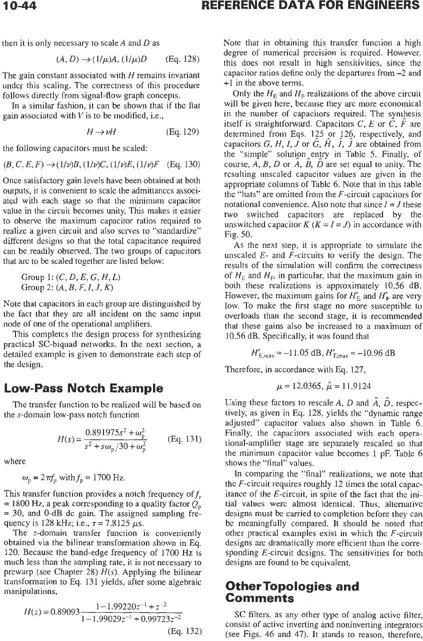
biquad is shown in Fig. 49, in which capital letters
A
through
L,
of course, identify capacitors.
This
circuit is
widely used throughout the industry. Because of space
limitations, only the salient properties of this circuit
will be highlighted. The interested reader is referred
to
the references for detailed derivations and demonstra-
tions of individual features.
It simplifies the general analysis of
this
biquad
to
assume the input,
Vh,
is sampled and held for the full
clock period. Although not necessary in every special-
case implementation of Fig. 49, the condition is
readily arranged. Furthermore, if the input to a cascade
of such
SC
biquads is presented with a full-clock-
period sampled-and-held signal, the switch timing in
the biquads will propagate this condition through the
entire filter. This condition is provided inherently by
LP02 and BPOl biquads for any properly band-limited
input signal.
Since, depending
on
the application, the desired
out-
put may be either at
V
or
V',
both the corresponding
transfer functions are of interest. They are derived as
H
=
V/V,,
=
-N/D
and
H'
=
V'/&
=
N'/D
(Eq.
1224
*
References
1
and
26.
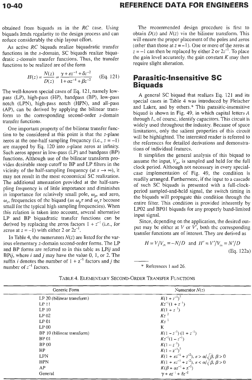
TABLE
4.
ELEMENTARY
SECOND-ORDER
TRANSFER
FUNCTIONS
Generic
Form
Numerator
N(z)
LP
20
(bilinear
transform)
LP
11
LP
10
LP
02
LP
01
LP
00
BP
10
(bilinear transform)
BP
01
BP
00
HP
LPN
HPN
Ap
General
K(l
+
Y1)*
Kz-'(l
+
z-I)
K(l
+
8)
Kz-'
Kz-'
K
K( 1
-
2')
(1
+
z-')
Kz-'(l
-
z-')
K(
1
-
z-')
K(
1
-
z-')'
K(l
+~Y~+z-~),~>af.,/-:p>O
K(l
+
EZ-'
+
z-~),
E
<
a/&,
p
>
0
K(p
+
aF1+
z-~)
y
+
&I1
+
82-2
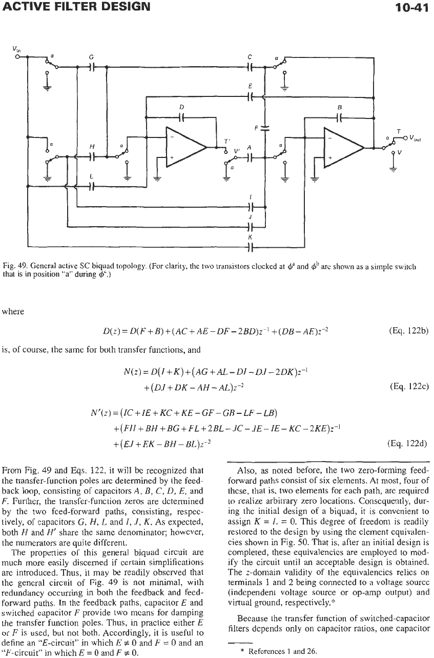
ACTIVE FILTER DESIGN
10-41
I
K
I
I1
Fig.
49.
General active
SC
biquad topology. (For clarity, the two transistors clocked at
@
and
+b
are
shown
as
a simple
switch
that
is
in
position “a” during
+‘.)
where
D(z)=
D(F+B)+(AC+AE-DF-~BD)~-‘+(DB-AE)Z-~
is, of course, the same for both transfer functions, and
N(z)=
D(I+K)+(AG+AL-DI-DJ-2DK)z-l
+
(DJ
+
DK
-
AH
-
AL)z-~
N’(z)
=
(IC
+
IE
+
KC
+
KE
-
GF
-
GB
-
LF
-
LB)
+(FH
+
BH
+
BG+ FL+2BL-
JC-
JE-
IE-
KC-2KE)z-’
+
(EJ
+
EK
-
BH
-
BL)z-~
(Eq. 122d)
(Eq. 122b)
(Eq. 122c)
From Fig.
49
and Eqs. 122, it will be recognized that
the transfer-function poles are determined by the feed-
back loop, consisting of capacitors A, B,
C,
D,
E,
and
F.
Further, the transfer-function zeros
are
determined
by the two feed-forward paths, consisting, respec-
tively, of capacitors G, H,
L
and
I,
J,
K.
As expected,
both
H
and
H‘
share the same denominator; however,
the numerators are quite different.
The properties
of
this general biquad circuit are
much more easily discerned if certain simplifications
are introduced. Thus, it may be readily observed that
the general circuit of Fig.
49
is not minimal, with
redundancy occurring
in
both the feedback and feed-
forward paths.
In
the feedback paths, capacitor E and
switched capacitor
F
provide two means for damping
the transfer function poles. Thus,
in
practice either
E
or
F
is used, but not both. Accordingly, it is useful to
define an “E-circuit’’ in which
E
#
0
and
F
=
0
and
an
“F-circuit” in which
E
=
0
and
F
#
0.
Also, as noted before, the two zero-forming feed-
forward paths consist of six elements. At most, four of
these, that is, two elements for each path, are required
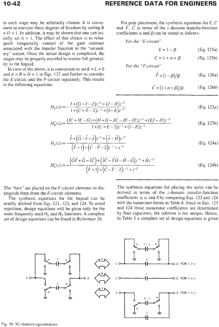
to realize arbitrary zero locations. Consequently, dur-
ing the initial design of a biquad, it is convenient
to
assign
K
=
L
=
0.
This degree
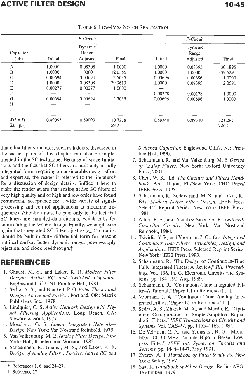
of
freedom is readily
restored to the design by using the element equivalen-
cies shown in Fig.
50.
That is, after an initial design is
completed, these equivalencies are employed to mod-
ify the circuit until an acceptable design is obtained.
The z-domain validity of the equivalencies relies
on
terminals
1
and 2 being connected
to
a voltage source
(independent voltage source or op-amp output) and
virtual ground, respectively.*
Because the transfer function of switched-capacitor
filters depends only
on
capacitor ratios, one capacitor
*
References
1
and
26.
10-42
REFERENCE
DATA
FOR ENGINEERS
in each stage may be arbitrarily chosen. It is conve-
nient to exercise these degrees of freedom by setting
B
=
D
=
1.
In addition, it may be shown that one can ini-
tially set
A
=
1.
The effect of this choice
is
to relin-
quish temporarily control of the gain constant
associated with the transfer function to the “second-
ary”
output. Once the initial design is completed, the
stages may be properly rescaled to restore full general-
ity to the biquad.
In view
of
the above, it is convenient to set
K
=
L
=
0
and
A
=
B
=
D
=
1 in
Eqs.
122 and further to consider
the E-circuit and the F-circuit separately. This results
in the following equations:
Fotpole placement, the synthesis equations for
E,
C
and
F,
C
in
terms of the z-domain transfer-function
coefficients
a
and
p
can be stated as follows:
For
the
“E-circuit”
E=1-P
(Eq.
125a)
c=1+a+p
(Eq.
125b)
For
the “F-circuit”
P
=
(1
-
P)/P
(Eq.
126a)
E
=
(1
+a
+
p)/p
(Eq.
126b)
I
+
(G
-
I
-J)z-’
+(I
-
H)z-~
1
+
(C
+
E
-
2)2-’+ (1
-
E)z-’
HE(z)
=
-
(IC+
IE
-
G)+(H
+
G-
JC-
JE
-IE)~-‘
+(EJ-
H)~-~
Hk(z)
=
1
+
(C
+
E
-
2)~-’+
(1
-
E)z-~
i
+
(G-
i
-+1+
(j
-
2)z-2
p
+
1)
+(E
-P-2)2-’+
2-2
(%+
6
-2)
+
[Z
-
P2
-
2
-
qz-1
(P+l)+(E-P-2
1
z-1
+z-2
HF(z)
=
-
H;(z)
=
-
~ ~~
(Eq.
123a)
(Eq.
123b)
(Eq.
124a)
(Eq.
124b)
The “hats” are placed on the F-circuit elements to dis-
tinguish them from the E-circuit elements.
The synthesis equations for the biquad can be
readily derived from Eqs. 121, 123, and 124. TO avoid
repetition, design equations will be given only for the
more frequently used
HE
and
HF
functions.
A
complete
set of design equations can be found in Reference 26.
The synthesis equations for placing the zeros Can be
derived in terms
of
the z-domain transfer-function
coefficients and 6bY Comparing
Eqs.
123 and 124
with the numerator
forms
in Table
4.
Since in
Eqs.
123
and 124 those numerator coefficients are determined
by four capacitors, the solution
is
not unique. Hence,
in
Table
5
a complete set
of
design equations is given
Fig.
50.
SC
element
equivalencies.
10-43
TABLE
5.
ZERO
PLACEMENT
FORMULAS
FOR
HE
AND
HF
Filter
Type
Design
Equations
Simple
Solution
I=J=IKI
LP
20
I
=
IKI
LP
11
LP
10
LP
02
LP
01
LP
00
BP
10
BP
01
BP
00
HP
HPN
and
LPN
Ap
(P
>
0)
General
(y
>
0)
G
-
I
-
J=
2
IKI
J-H=IKI
I=0
G
-
I
-
J
=
kIKI
J-H=
kIKI
I
=
IKI
G
-I
-
J
=
IKI
J-H=O
I=O
G-I-J=O
J-
H
=
*IKI
I=O
G
-I
-
J=
+IM
J-H=O
I=IM
G-I-J=O
J-H=O
I
=
IKI
G-I-J=O
J-
H
=
-IKI
I=O
G
-
I
-
J
=
+IKI
J- H
=
+IK1
I
=
IKI
G
-
I
-
J
=
-/Kl
J-H=O
I=IM
G
-
I
-
J=
-21M
J-H=IKI
I=IM
G
-I
-J
=
IKk
J-
H
=
IKI
I
=
IKlP
J-H=IKI
G
-I-
J
=
lKla
I=
y
G-I-J=&
J-H=S
G=4
IM,
H=
0
I
= 0,
J
=
IKI
G
=
2
IKI, H
=
0
I
=
IKI,
J
=
0
G
=
2
IKI,
H=
0
Z=J=O
G
=
0.
H= IKI
I=J=O
G
=
IKI,
H
=
0
I
=
IKI,
J
=
0
G
=
IKI,
H
=
0
I
=
IKI,
J
=
0
G
=H
=
IKI
I
=
0,
J=
IKI
G=H=O
I
=
IKI,
J
=
0
G=H=O
I=J=IKI
G=H=O
I=J=IKI
G
=
IKl(2
+
E),
H
=
0
I
=
IKIP, J
=
IKI
G
=
IKI(1
+
P
+
a)
=
lMC
H=O
J=S+x
G=y+S+c+x
H=xtO
I=
y
Note:
&=G(1
+
k),
H=H(1
+
k),
i=
I(1
+
k),
and
j=
.?(I
+
k).
for each case. For each
of
the cases, a “simple”
solu-
tion is also offered.
The synthesis equations given in the previous para-
graphs result in unscaled capacitor values.
To
complete
the
synthesis in practice, some scaling is required. The
first order
of
business is to adjust the voltage level at
the “secondary” output.
If
this voltage
is
too high,
amplifier overloads may result; if it is too
low,
unnec-
essary noise penalties may be taken.
Although the voltage levels and necessary scaling
factors may be obtained by using analysis techniques,”
the
simplest procedure is to simulate the unscaled cir-
cuit on an analysis program. This method serves
also
as a confirmation
of
the
correctness of the design.
To
adjust the voltage level
V’,
i.e., the flat gain
of
H’,
without affecting
H,
only capacitors
A
and
D
need to
be scaled. More precisely, if it is desired
to
modify the
gain constant associated
with
V’
according
to
H’+
1.H’
(Eq.
127)
*
Reference
1.
then it is only necessary to scale
A
and
D
as
(AD)
+
(llp)A,
(l/p)D
0%.
128)
The gain constant associated with
H
remains invariant
under this scaling. The correctness of this procedure
follows directly from signal-flow graph concepts.
In a similar fashion, it can be shown that if the flat
gain associated with
V
is to be modified, i.e.,
H+vH
(Eq.
129)
the following capacitors must be scaled:
(B,
C,
E,
0
-+
(llvIB, (llv)C,
(llv)E,
(1lv)F
(Eq.
130)
Once satisfactory gain levels have been obtained at both
outputs, it is convenient to scale
the
admittances associ-
ated with each stage
so
that the minimum capacitor
value in the circuit becomes unity.
This
makes it easier
to observe the maximum capacitor ratios required to
realize a given circuit and also serves to “standardize”
different designs
so
that the total capacitance required
can be readily observed. The two groups of capacitors
that are to be scaled together are listed below:
Group
1:
(C,
D,
E,
G,
H,
L)
Group
2:
(A,
B,
F,
I,
J,
K)
Note that capacitors in each group are distinguished by
the fact that they are all incident
on
the same input
node of one of the operational amplifiers.
This completes the design process for synthesizing
practical SC-biquad networks.
In
the next section, a
detailed example is given to demonstrate each step of
the design.
Low-Pass
Notch
Example
The transfer function to be realized will be based on
the s-domain low-pass notch function
0.891975s’
+w;
H(s)
=
(Eq.
131)
s2
+
swp/30
+
w,”
where
wp
=
2nfjP
with
fp
=
1700
Hz.
This
transfer function provides a notch frequency off,
=
1800
Hz,
a
peak corresponding
to
a
quality factor
Qp
=
30,
and 0-dB dc gain. The assigned sampling fre-
quency is
128
kHz;
Le.,
T=
7.8125
ps.
The z-domain transfer function is conveniently
obtained via the bilinear transformation shown in Eq.
120.
Because the band-edge frequency of
1700
Hz is
much less than the sampling rate, it is not necessary to
prewarp (see Chapter
28)
H(s).
Applying the bilinear
transformation to Eq.
131
yields, after some algebraic
manipulations,
1
-
1.992202-‘
+
z-’
1
-
1.990292-’
+
0.99723~-’
H(z)
=
0.89093
(Eq.
132)
Note that in obtaining this transfer function a high
degree of numerical precision is required. However,
this does not result in high sensitivities, since the
capacitor ratios define only the departures from
-2
and
+1
in
the above terms.
Only the
HE
and
HF
realizations of the above circuit
will be given here, because they are more economical
in the number of capacitors required. The synthesis
itself is straightforward. Capacitors
C,
E
or
C,
F
are
determined from Eqs.
1?5
,Or
j2$,
respectively, and
capacitors
G,
H,
I,
J
or
G,
H,
I,
J
are
obtained from
the “simple” solutipAenApy in Table
5.
Finally, of
course,
A,
B,
D
or
A,
8,
D
are set equal to unity. The
resulting unscaled capacitor values are given in the
appropriate columns of Table
6.
Note that
in
this table
the “hats” are omitted from the F-circuit capacitors for
notational convenience.
Also
note that since
I
=
J
these
two switched capacitors
are
replaced by the
unswitched capacitor
K
(K =I
=
J)
in accordance with
Fig.
50.
As
the next step, it is appropriate to simulate the
unscaled E- and F-circuits to verify the design. The
results of the simulation will confirm the correctness
of
HE
and
HF,
in particular, that the maximum gain
in
both these realizations is approximately
10.56
dB.
However, the maximum gains for
Hk
and
HL
are very
low. To make the first stage no more susceptible to
overloads than the second stage, it is recommended
that these gains also be increased to a maximum of
10.56
dB. Specifically, it was found that
-1 1.05
dB,
HL,,max
=
-10.96
dB
Therefore, in accordance with Eq.
127,
p
=
12.0365,
fi
=
11.9124
Using these factors to rescale
A,
D
and
2,
b,
respec-
tively, as given in Eq.
128,
yields the “dynamic range
adjusted” capacitor values also shown in Table
6.
Finally, the capacitors associated with each opera-
tional-amplifier stage
are
separately rescaled
so
that
the minimum capacitor value becomes
1
pF. Table
6
shows the “final” values.
In
comparing the “final” realizations, we note that
the F-circuit requires roughly
12
times the total capac-
itance of the E-circuit, in spite of the fact that the ini-
tial values were
almost
identical.
Thus,
alternative
designs must be carried
to
completion before they can
be meaningfully compared. It should be noted that
other practical examples exist
in
which the F-circuit
designs are dramatically more efficient than the corre-
sponding E-circuit designs. The sensitivities for both
designs
are
found to be equivalent.
Other Topologies and
Comments
SC filters, as any other type of analog active filter,
consist
of
active inverting and noninverting integrators
(see Figs.
46
and
47).
It stands to reason, therefore,
10-45
TABLE
6.
LOW-PASS NOTCH REALIZATION
E-Circuit F-Circuit
Dynamic Dynamic
Capacitor
Range
Range
(PF)
Initial Adiusted Final Initial Adiusted Final
A
B
C
D
E
F
G
H
I
J
K(I
=
J)
CC
(PF)
1
.oooo
I
.oooo
0.00694
1
.oooo
0.00277
0.00694
-
-
-
-
0.89093
-
0.08308
1
.oooo
0.00694
0.08308
0.00277
0.00694
-
-
-
-
0.89093
-
1
.oooo
12.0365
2.5035
29.9613
1
.oooo
2.5035
-
-
-
-
10.7238
59.7
1
.oooo
1.0000
0.00696
1
.oooo
0.00278
0.00696
-
-
-
-
0.89340
-
0.08395
1.0000
0.00696
0.08395
0.00278
0.00696
-
-
-
-
0.89340
-
30.1895
1.0000
12.0591
1
.oooo
I
.oooo
359.629
-
-
-
-
321.293
726.1
that other filter structures, such as ladders, discussed in
the earlier parts of
this
chapter can also be imple-
mented in the SC technique. Because of space limita-
tions and the fact that SC filters are built only in fully
integrated form, requiring a considerable design effort
and expertise, the reader is referred
to
the literature*
for a discussion of design details. Suffice it here to
make the reader aware that analog active
SC
filters of
very high quality and of high and low order have found
commercial acceptance for a wide variety of signal-
processing and control applications at moderate fre-
quencies. Attention must be paid only to the fact that
SC filters are sampled-data circuits, which calls for
some care in the system design. Finally, we emphasize
again that integrated SC filters,
just
as
g,-C
circuits,
should be built in fully differential form for reasons
outlined earlier: better dynamic range, power-supply
rejection, and clock feedthr0ugh.t
REFERENCES
1.
Ghausi, M.
S.,
and Laker,
K.
R.
Modern Filter
Design: Active RC and Switched Capacitor.
Englewood Cliffs, NJ: Prentice Hall,
1981.
2.
Sedra,
A.
S.,
and Brackett, P.
0.
Filter Theory and
Design: Active and Passive.
Portland,
OR
Matrix
Publishers, Inc.,
1978.
3.
Lindquist, C.
S.
Active Network Design with Sig-
nal Filtering Applications.
Long
Beach, CA:
Steward
&
Sons,
1977.
4.
Moschytz, G.
S.
Linear Integrated Network-
Design.
New York: Van Nostrand Reinhold,
1975.
5.
Van Valkenburg,
M.
E.
Analog Filter Design.
New
York Holt, Rinehart and Winston,
1982.
6.
Schaumann, R., Ghausi, M.
S.,
and Laker, K. R.
Design
of
Analog Filters: Passive, Active RC and
*
References
1,6,
and
24-27.
7
Reference
27.
7.
8.
9.
10.
11.
12.
13.
14.
15.
Switched Capacitor.
Englewood Cliffs, NJ: Pren-
tice Hall,
1990.
Schaumann,
R.,
and Van Valkenburg,
M.
E.
Design
of
Analog Filters.
New York Oxford University
Press,
2001.
Chen, W.
K.,
Ed.
The Circuits and Filters Hand-
book.
Boca Raton, FL/New York CRC Press/
BEE Press,
1995.
Schaumann, R., Soderstrand, M.
S.,
and Laker, R.,
Eds.
Modern Active Filter Design.
IEEE Press
Selected Reprint Series. New York: IEEE Press,
1981.
Allen, P. E., and Sanchez-Sinencio, E.
Switched-
Capacitor Circuits.
New York: Van Nostrand
Reinhold,
1984.
Tsividis,
Y.
P.,
and
Voorman, J.
O.,
Eds.
Integrated
Continuous-Time Filters-Principles, Design, and
Applications.
IEEE Press Selected Reprint Series.
New York: EEE Press,
1993.
Schaumann, R. “The Design of Continuous-Time
Fully Integrated Filters: A Review,”
ZEE Proceed-
ings,
Vol.
136,
Pt. G, Electronic Circuits and Sys-
tems, pp.
184-190,
Aug.
1989.
Schaumann, R. “Continuous-Time Integrated Fil-
ter-A Tutorial,” Paper
l. l
in Reference
[
1
l].
Voorman, J. A. “Continuous-Time Analog Inte-
grated Filters,” Paper
l
.2
in Reference
[
l l].
Sedra, A.
S.,
Zharab,
M.
A., and
Martin,
K.
“Opti-
mum Configuration
of
Single-Amplifier
Biqua-
dratic Filters,”
IEEE Transactions
on
Circuits and
Svstems,
Vol.
CAS-27,
vu.
1155-1163, 1980.
16.
De Veirman, G. A., and Yamasaki, R. G. “Mono-
lithic
10-30
MHz Tunable Bipolar Bessel Low-
pass Filter,”
ZEEE Znt. Symp.
on
Circuits and
Systems,
pp.
1444-1447,
May
1991.
17.
Zverev, A.
I.
Handbook
of
Filter Synthesis.
New
York Wiley,
1967.
18.
Saal R.
Handbook
of
Filter Design.
Berlin: AEG-
Telefunken,
1979.
19.
Wu,
P.. and Schaumann, R. “A 200 MHz Elliptic
OTA-C Filter in GaAs Technology,”
Proc. IEEE
Int. Symp. on Circuits and Systems,
pp. 1745-
1748, June 1991.
20. Tan, M. A., and Schaumann, R. “Simulating Gen-
eral-Parameter LC-Ladder Filters for Monolithic
Realizations with Only Transconductance Ele-
ments and Grounded Capacitors,”
IEEE Transac-
tions
on
Circuits and Systems,
Vol. CAS-36,
No.
2,
pp. 299-307, Feb. 1989.
21. Snelgrove,
W.
M., and Sedra, A.
S.,
“Optimization
of
Dynamic Range in Cascade Active Filters,”
Proc. IEEE Int. Symp. on Circuits and Systems,
22. Chiou, C.
E,
and Schaumann, R. “Comparison
of
Dynamic Range Properties
of
High-Order Active
Bandpass Filters,”
Proc. IEE,
Vol. 127, Pt. G,
Electronic Circuits and Systems,
No.
3, pp. 101-
108, 1980.
23.
Khoury,
J.
M. “Design of a 15-MHz CMOS Con-
tinuous-Time Filter with On-Chip Tuning,”
IEEE
pp. 151-155, 1978.
Journal on Solid State Circuits,
Vol. SC-26,
No.
24. Gray,
P.
R., Hodges, D. A., and Broderson, R.
W.,
Eds.
Analog
MOS
Integrated Circuits,
IEEE Press
Selected Reprint Series, 1980.
25. Martin,
K.,
and Sedra, A.
S.
“Effects of Op Amp
Finite Gain and Bandwidth on the Performance
of
Switched Capacitor Filters,”
IEEE Transactions
on
Circuits and Systems,
Vol. CAS 28, pp. 822-
829, Aug. 1981.
26. Fleischer,
P.
E.,
and Laker,
K.
R.
“A Family of
Active Switched-Capacitor Biquad Building
Blocks,”
The Bell System Technical Journal,
Vol.
58,
No.
10, Dec. 1979. (Reprinted in [9])
27. Choi, T. C., et al. “High-Frequency CMOS
Switched-Capacitor Filters for Communications
Applications,”
IEEE J. Solid-state Circuits,
Vol.
32-18, pp. 652-664, Dec. 1983.
28. Li, D., and Tsividis,
Y.
“Active LC Filters
on
Sili-
con,”
IEE Proceedings-Circuits,
Devices and Sys-
tems, Vol. 147,
No.
1, pp. 49-56, Feb. 2000.
12, pp. 1988-1997,1991,
11
Attenuators
Revised
by
Bruno
0.
Weinschel
Definitions
I1
-2
Typical Designs of Resistive Attenuators
Resistance Networks for Attenuators
Power Dissipation Within a Tee Pad
1
1-2
Connectors
I1
-4
Measurement
of
Attenuation
1
1-4
Fixed-Frequenc
y
Broadband
Swept or Stepped in Frequency
11-1
11-2
REFERENCE DATA FOR ENGINEERS
DEFINITIONS
An attenuator
is
a network that reduces the input
power by a predetermined ratio. The ratio of input
power to output power is expressed in logarithmic terms
such as decibels (dB).
Attenuation in dB
=
10 loglo
flnlPout
E
20 loglo
Ei,lEout
NOTE:
ZSOU~C~
=
zload
=
Zattenuatoi
All resistive, matched
Examples:
1)
P,,lP,,,
=
13.18
=
10
X
1.318
10 log~oP,,lP,,~ dB
=
10
(log10 10
+
loglo 1.318) dB
=
lO(1
+
0.1199) dB
=
11.2 dB
2)
Ein/Eout
=
3.630
20 loglo
Ei,lEout
dB
=
20 loglo 3.630 dB
=
20
X
0.560
dB
=
11.2 dB
To convert attenuation in decibels into power or voltage
ratio:
PinlPou,
=
logl0-l dBllO
=
IOdB'"
Ei,lEoul
=
loglo-' dBl20
=
10dB'20
Examples
:
3) 11.2 dB
Pin/Poul
=
10"
2110
=
4)
11.2 dB
EinlE,,,
=
10".2/20
=
Table
1
lists a few decibel values together with the
corresponding power and voltage ratios.
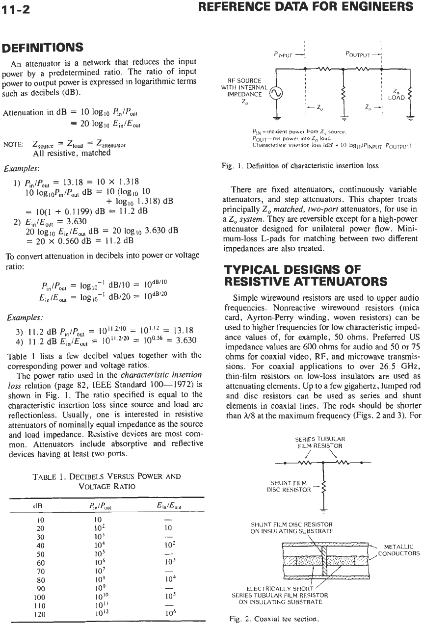
The power ratio used in the
characteristic insertion
loss
relation (page 82,
IEEE
Standard 100-1972) is
shown in Fig.
1.
The ratio specified is equal to the
characteristic insertion
loss
since source and load are
reflectionless. Usually, one is interested in resistive
attenuators of nominally equal impedance as the source
and load impedance. Resistive devices are most com-
mon. Attenuators include absorptive and reflective
devices having at least two ports.
=
13.18
=
3.630
TABLE
1. DECIBELS VERSUS POWER
AND
VOLTAGE RATIO
10
20
30
40
50
60
70
80
90
100
110
120
10
lo2
103
io4
io5
1
o6
107
108
109
10'0
10"
10'2
-
10
-
102
103
104
105
-
-
-
-
106
I I
I
PINPUT
-:
POUTPUT
I
I
1
I
I
RF SOURCE
I
PIN
=
incident
power
from
Z,,
SOUTCP
POUT=
net
power
into
Z,
ioad
Characteristic
insertion
loss idB)
=
10
logll,lPlhpliT
PoUTpUT]
Fig.
1.
Definition
of
characteristic insertion
loss.
There are fixed attenuators, continuously variable
attenuators, and step attenuators. This chapter treats
principally
Z,
matched,
two-port
attenuators, for use in
a
Z,
system.
They are reversible except for a high-power
attenuator designed for unilateral power flow. Mini-
mum-loss L-pads for matching between two different
impedances
are
also treated.
TYPICAL DESIGNS OF
RESISTIVE ATTENUATORS
Simple wirewound resistors are used to upper audio
frequencies. Nonreactive wirewound resistors (mica
card, Ayrton-Perry winding, woven resistors) can be
used to higher frequencies for low characteristic imped-
ance values of, for example,
50
ohms. Preferred US
impedance values
are
600
ohms for audio and
50
or 75
ohms for coaxial video, RF, and microwave transmis-
sions. For coaxial applications to over 26.5
GHz,
thin-film resistors on low-loss insulators are used as
attenuating elements. Up to a few gigahertz, lumped
rod
and disc resistors can be used as series and shunt
elements in coaxial lines. The rods should be shorter
than
AI8
at the maximum frequency (Figs. 2 and 3). For
SERIES TUBULAR
FILM RESISTOR
/\
SHUNT FILM
3Hll?-T
FILM DISC RCSiSIOR
ON
IhSbLi\
I
IN6
bU8STRATF
\
\
METALLIC
CONDUCTORS
ELECTRICALLY
StiOR:
/
SERIES TUBULAR FILM RESISTOR
ON INSULATING SUBSTRATE
Fig.
2.
Coaxial
tee
section.
ATTENUATORS
11-3
SERIES TUBULAR
FILM RESISTOR
\
SHUNT FILM DISC RESISTOR
ON INSULATING SUBSTRATE
ELECTRICALLY SHORT METALLIC
SERIES TUBULAR FILM RESISTOR CONDUCTORS
ON INSULATING SUBSTRATE
Fig.
3.
Coaxial pi section.
higher frequencies, distributed resistive films on sus-
pended substrates are used (Fig.
4).
Resistance Networks
for
Attenuators
Four types
of
symmetrical pads
are
shown in Fig.
5.
The formulas for the resistance values in ohms for these
pads when
R,
=
1
ohm are given below. If R, has a
value other than
1
ohm, multiply each of the resistance
values
(u,
b,
c,
]/a,
Ilb,
and l/c) by
R,.
An unsymmetrical matching pad is shown in Fig.
6.
The formulas for this pad are:
J
=
Rl
-
kR,/(k
+
R,)
k
=
[RlR3/(R1
-
R2)]1’2,
where
Rl
>
R2
Minimum loss in
dB
=
20 loglo{[(RI
-
R2)/R2]1’2
+
(R
IR,)
’’*}
Typical values for the pads in Fig.
5
are listed in
Table 2. Typical values for the pad in Fig.
6
are listed in
Table
3.
Balanced pads are used in balanced transmission
lines. For voice,
Z,
is
typically
600
ohms; for VHF TV,
Z,
is typically
300
ohms. Bridged tee pads are common
in low-frequency step attenuators. Lumped-element pi
pads are short and easily matched up to about
1.5
GHz,
with
75-
or 50-ohm impedance. Coaxial tee pads of
%-ohm impedance can work above
10
GHz if the series
elements are short in comparison with the wavelength.
For low frequency sensitivity, thin resistive films (Ni-
66
9
I1
I
(A)
6
dB
tee
section--50
ohms.
(5)
SIX
I
dB
tee
sectlons
In
serles--50
ohms.
LOW RESISTANCE LAUlLCHlhG
AND RECEIVING ELECTRODES
LOW RESISTANCE
GROUND ELECTRODES
RESISTIVE FILM
OK
INSULATING SUBSTRATE
(C)
Dlstrlbuted
serles
and
shunt
reslrton.
Fig.
4.
Distributed series and shunt resistive attenuator element
on
suspended substrate in coaxial line.