Middleton W.M. (ed.) Reference Data for Engineers: Radio, Electronics, Computer and Communications
Подождите немного. Документ загружается.

10-30
REFERENCE
DATA
FOR ENGINEERS
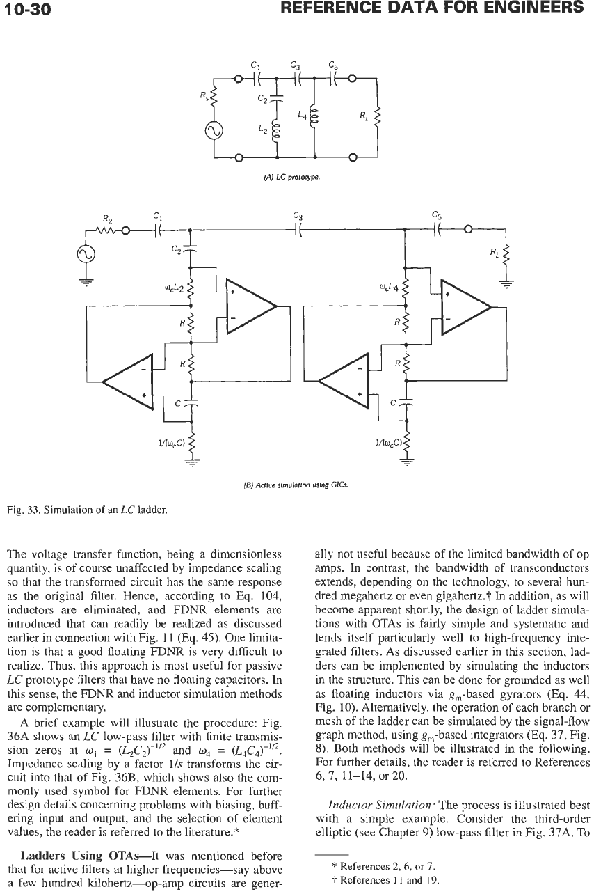
(A)
LC
prototype
(Bj
Actlve
slrnulotlon
uslng
GlCs
Fig.
33.
Simulation
of
an
LC
ladder.
The voltage transfer function, being a dimensionless
quantity, is
of
course unaffected by impedance scaling
so
that the transformed circuit has the same response
as the original filter. Hence, according to Eq. 104,
inductors are eliminated, and FDNR elements
are
introduced that can readily be realized as discussed
earlier in connection with Fig.
11
(Eq. 45). One limita-
tion
is
that a good floating FDNR is very difficult
to
realize. Thus, this approach is most useful for passive
LC
prototype filters that have no floating capacitors. In
this sense, the FDNR and inductor simulation methods
are complementary.
A brief example will illustrate the procedure: Fig.
36A shows an
LC
low-pass filter with finite transmis-
sion zeros at
w1
=
(L,C,)-1/2
and
o4
=
(L4C4)-”*.
Impedance scaling by a factor
l/s
transforms the cir-
cuit into that of Fig.
36B,
which shows also the com-
monly used symbol for FDNR elements. For further
design details concerning problems with biasing, buff-
ering input and
output, and the selection of element
values, the reader is referred to the literature.*
Ladders
Using OTAs-It was mentioned before
that for active filters at higher frequencies-say above
a few hundred kilohertz-op-amp circuits are gener-
ally not useful because of the limited bandwidth of
op
amps.
In
contrast, the bandwidth of transconductors
extends, depending on the technology, to several hun-
dred megahertz or even gigahertz.?
In
addition, as will
become apparent shortly, the design of ladder simula-
tions with
OTAs
is fairly simple and systematic and
lends itself particularly well
to
high-frequency inte-
grated filters.
As
discussed earlier in this section, lad-
ders can be implemented by simulating the inductors
in the structure. This can be done for grounded as well
as floating inductors via g,-based gyrators (Eq.
44,
Fig.
10).
Alternatively, the operation of each branch or
mesh of the ladder can be simulated by the signal-flow
graph method, using g,-based integrators
(Eq.
37, Fig.
8).
Both methods will be illustrated in the following.
For further details, the reader is referred to References
6,7, 11-14, or
20.
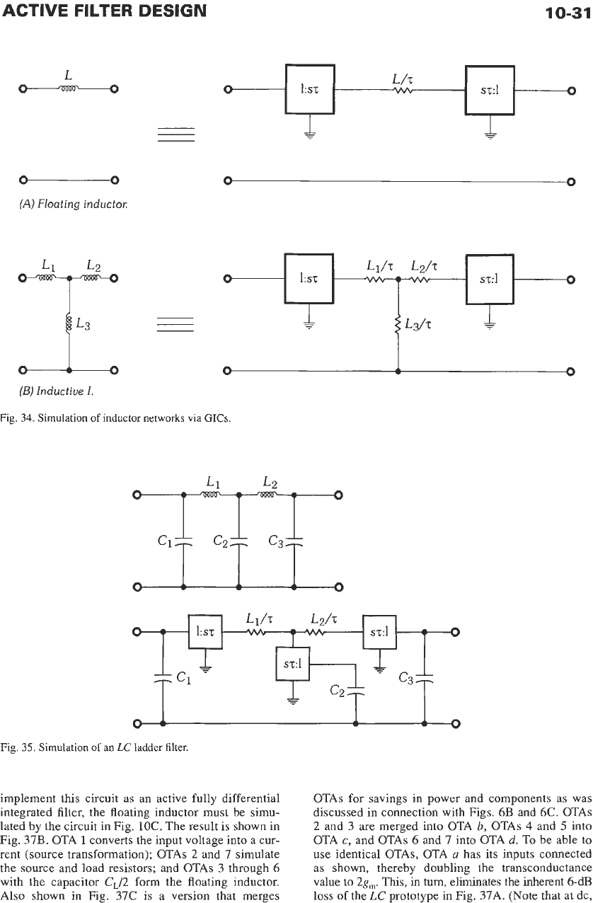
Inductor
Simulation: The process
is
illustrated best
with a simple example. Consider the third-order
elliptic (see Chapter
9)
low-pass filter in Fig. 37A. To
*
References
2,6,
or
7.
t
References
11
and
19.
ACTIVE
FILTER
DESIGN
10-31
-0
(A)
Floating inductor
i
L3
i,
(B)
Inductive
I.
Fig. 34.
Simulation
of
inductor networks via
GICs.
Fig.
35.
Simulation
of
an
LC
ladder filter.
implement this circuit as an active fully differential
integrated filter, the floating inductor must be simu-
lated by the circuit in Fig. 1OC. The result is shown in
Fig. 37B. OTA
1
converts the input voltage into a cur-
rent (source transformation); OTAs
2
and
7
simulate
the source and load resistors; and OTAs 3 through
6
with the capacitor
CJ2
form the floating inductor.
Also shown in Fig. 37C is a version that merges
OTAs for savings in power and components as was
discussed in connection with Figs. 6B and 6C. OTAs
2
and 3 are merged into OTA
b,
OTAs
4
and
5
into
OTA
c,
and
OTAs
6 and 7 into OTA
d.
To
be
able to
use identical OTAs, OTA
a
has its inputs connected
as shown, thereby doubling the transconductance
value to
2g,.
This,
in
turn,
eliminates the inherent 6-dB
loss
of
the
LC
prototype in Fig. 37A. (Note that at dc,
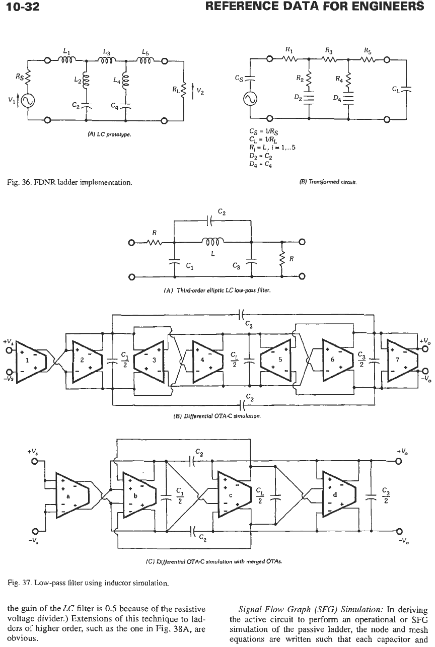
10-32
R
REFERENCE
DATA
FOR ENGINEERS
0
L
--
_-
R
--
Cl
c3
--
(A)
LC
prototype
Fig.
36.
FDNR
ladder implementation.
c,
=
I/Rs
CL
=
Zm;
D:,
=
C,
D,
=
C,
Ri
=
Li,
i
=
1,
...
5
(E)
Transformed circuit.
+
"s
0
0
-vs
(BJ
Differential
OTA-C
simulation.
fCJ
Differential
OTA-C
simulation with merged
OTAs.
Fig.
37.
Low-pass
filter
using inductor simulation.
the gain
of
the
LC
filter is
0.5
because
of
the resistive
voltage divider.) Extensions
of
this technique to lad-
ders
of
higher order, such
as
the one in Fig.
38A,
are
obvious.
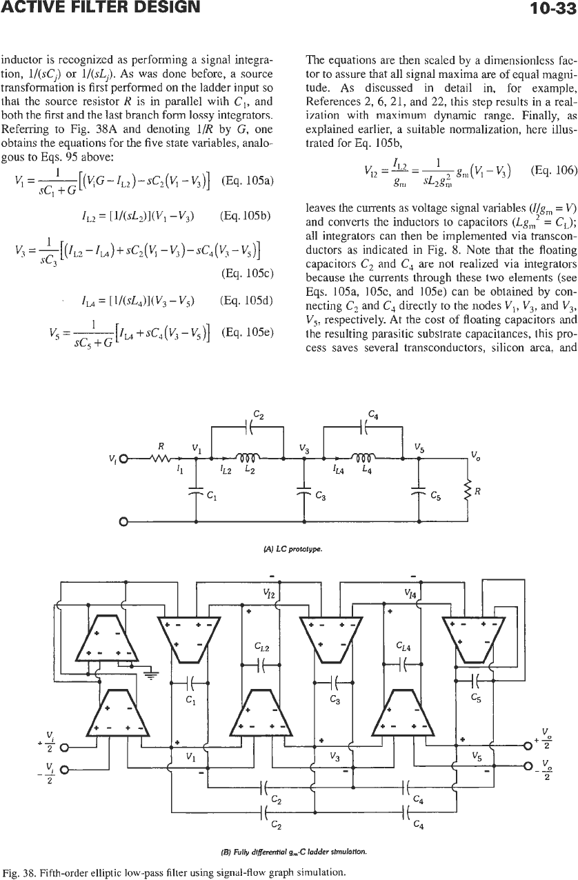
Signal-Flow Graph (SFG) Simulation:
In
deriving
the active circuit to perform
an
operational
or SFG
simulation
of
the passive ladder, the node and mesh
equations are written such that each capacitor and
ACTIVE
FILTER
DESIGN
10-33
inductor is recognized as performing a signal integra-
tion, l/(sCj)
or
l/(sLj).
As
was done before, a source
transformation is first performed on the ladder input so
that the source resistor R
is
in parallel with
C,,
and
both the first and the last branch form lossy integrators.
Referring to Fig.
38A
and denoting 1/R by
G,
one
obtains the equations for the five state variables, analo-
gous
to
Eqs.
95
above:
1
sCl
+G
V,
=-[(~G-ZL,)-sCz(V,
-V3)]
(Eq. 105a)
IL2
=
[~/(sLJ](V~
-V3)
(Eq. 10%)
The equations
are
then scaled by a dimensionless fac-
tor to assure that all signal maxima are
of
equal magni-
tude.
As
discussed
in
detail in, for example,
References
2,
6, 21, and
22,
this
step results in a real-
ization with maximum dynamic range. Finally, as
explained earlier, a suitable normalization, here illus-
trated for Eq. 105b,
leaves the currents as voltage signal variables
(Z/g,,,
=
V)
and converts the inductors
to
capacitors
(Lg,’
=
CL);
all integrators can then be implemented via transcon-
ductors as indicated in Fig.
8.
Note that the floating
capacitors
C,
and
C,
are not realized via integrators
because the currents through these two elements (see
Eqs. 105a, 105c, and 105e) can be obtained by con-
necting
C,
and
C,
directly to the nodes
V,, V,,
and
V3,
V,,
respectively.
At
the cost
of
floating capacitors and
the resulting parasitic substrate capacitances, this pro-
cess saves several transconductors, silicon area, and
f
c,
(A)
LC
prototype.
V
Fig.
38
(B)
Fully
dlferentlal
g,-C
ladder simulatton.
.
Fifth-order
elliptic low-pass
filter
using signal-flow graph simulation.
power and reduces noise. Making use of multiple-
input transconductors to achieve a fully differential
circuit, the five equations (Eqs. 105) are implemented
step by step, and interconnected
as
indicated in Fig.
38B. The normalized signal voltages, representing the
state variables
V12, VI,,
VI,
V,,
and
V,,
are marked in
Fig. 38B for easy reference.
Observe that the ladder simulation technique leads
to
a
very efficient and systematic active realization of
the passive prototype. The fifth-order active ladder
requires five two-input summing transconductors, plus
two
for simulating the source and load resistors, and
five capacitors, plus two for each floating
C
in the pas-
sive prototype. All transconductors are identical.
Again,
it
should be apparent how the method is
extended
to
filters of higher order.
SWITCHED-CAPACITOR
FILTERS
Metal-oxide-semiconductor (MOS) integrated cir-
cuit (IC) technology
is
used widely in industry because
of its superior logic density and lower power consump-
tion compared to that achievable with other
IC
tech-
nologies. With very large scale integration
(VLSI),
hundreds of thousands to millions of MOS transistors
can be placed on a single chip. The ubiquitous pres-
ence of CMOS chips in appliances, entertainment elec-
tronics, and personal computers indicates the
economic and social impact
of
MOS
VLSI
on modern
society.
Switched-capacitor (SC) techniques, in addition to
the
g,-C
circuits discussed earlier, provide analog sig-
nal processing capability that
is
needed
in
MOS tech-
nology for “mixed-mode’’ analog/digital signal
processing requirements. The marriage of analog
SC
functions and high-density digital logic on the same
piece of silicon extends to mixed-mode systems the
same cost and space savings associated with memories
and microcomputers. One advantage of properly
designed
SC
filters over
g,-C
implementations is that
the realized characteristics usually require no trim-
ming and are inherently stable over process and envi-
ronmental variations. However, because of their
sampled-data nature, at the time of this writing, SC fil-
ters are commercially useful only at relatively moder-
ate frequencies (from the audio range up to possibly a
few hundred kilohertz), whereas continuous-time (c-t)
g,-C
circuits can be made to operate commercially at
several tens and even hundreds of megahertz. Conse-
quently, these two integrated analog filter design tech-
niques rarely compete in the same applications.
SC filters* consisting of
MOS
capacitors, switches,
and op amps realize infinite impulse response
(IIR)
analog sampled-data filters, similar topologically to
the active
RC
filters described
in
previous sections.
Narrow and flat passbands can be realized efficiently.
*
References
1,6,7,
10,24,
and
25.
Unlike their c-t active
RC
and
g,-C
counterparts,
SC
filters are sampled-data systems. This complicates
their use and design, but SC filters do indeed take full
advantage of the inherent precision achieved by
MOS
technology. As shown later, the transfer functions are
completely determined by precise crystal-controlled
clocks and capacitor ratios. Capacitor ratios can be
held
to
an accuracy
of
about
0.3
percent or less and,
with appropriate parasitics insensitive circuit tech-
niques,? capacitors
as
small as
0.2
pF can be used.
Furthermore,
MOS
capacitors are nearly ideal, with
very low dissipation factors and good temperature sta-
bility. These properties can be achieved with either
NMOS
or CMOS processing, but CMOS, with its
added flexibility for realizing high-gain, low-noise op
amps and low power dissipation, is recognized as the
technology of choice.
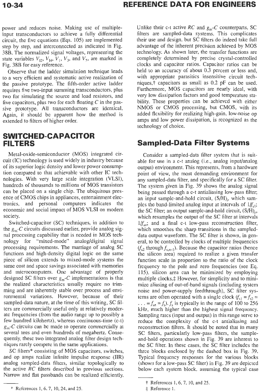
Sampled-Data Filter Systems
Consider a sampled-data filter system that is suit-
able for use in a c-t analog (i.e., analog input/analog
output) environment. This represents, from
a
hardware
point
of
view, the most demanding environment for
any sampled-data filter, and specifically for
a
SC
filter.
The system given in Fig. 39 shows the analog signal
being passed through
a
c-t antialiasing low-pass filter;
an input sample-and-hold circuit,
(SEI),,
which sam-
ples the band-limited analog input
at
intervals of
lRs1;
the
SC
filter;
an
output sample-and-hold circuit,
(SEI),,
which resamples the output of the SC filter at intervals
lNsfl; and a final c-t low-pass reconstruction filter,
which smoothes the sharp transitions
in
the sampled-
data output waveform. The SC filter is shown, in gen-
eral, to be controlled by clocks of multiple frequencies
(fs2
throughf,,,,). Because the capacitor ratios (hence
the silicon area) required to realize
a
given transfer
function scale in proportion to the ratio of the clock
frequency to the pole and zero frequencies (see Eq.
115), silicon area can be minimized by employing
multiple clocks.$ However, for simplicity and to
mini-
mize aliasing of out-of-band signals (including system
noise and power-supply feedthrough), SC filter sys-
tems are often operated with
a
single clock
(fsl
=fr2
=
.
.
.
=f,,
=f,).f,
is
typically in the range
of
100
to
256
kHz,
much higher than the highest signal frequency.
Sampling rates (input and output) in this range serve to
reduce the complexity of the c-t antialiasing and
reconstruction filters.
It
should be noted that in many
SC filters, particularly low-pass filters, the sample-
and-hold operations shown in Fig. 39 are inherent to
the
SC
filter. In these cases, the
SC
filter includes the
three blocks enclosed by the dashed box in Fig. 39.
Typical frequency responses for the various blocks
(shown for
a
low-pass SC filter) in Fig. 39 are depicted
below each system block. assuming the typical case
-
t
References
1,6,7,
10,
and
25.
$
Reference
1.
ACTIVE
FILTER
DESIGN
10-35
Fig.
39.
Sampled-data filter
system
for continuous-time analog input and smooth analog output.
that all clock frequencies are the samefsi
=fs,
i
=
I,
...,
n.
It is noted that when an input or output is interfaced
with digital or sampled-data circuitry, such as D/A and
A/D converters, some of this circuitry is no longer
needed. For example, when the output is to be inter-
faced to another sampled-data function, the recon-
struction filter is not required, and a sample-and-hold
circuit is typically included at the input of this func-
tion. Although the need for c-t filtering is reduced,
interfacing to digital and sampled-data circuits
requires careful synchronization between the clocks
that control the SC filter and those that control the
external sampling operations. This is accomplished by
passing synchronization pulses between the
SC
net-
work and the external samplers. One reason for syn-
chronization is to ensure that the
SC
network output is
sampled after all transients have settled and the output
is
steady.
Another consequence of the sampled-data character
of SC networks is the mathematical convenience of the
z
transform in analyzing or specifying SC filters. The
z
transform, where
z
=
exp
($7)
and
r
is the clock period,
is
covered in Chapter 28
(or
refer to References
I,
6-8,
or
10)
as a mathematical tool for digital filters and dis-
crete-time systems. The sampling instants, the instants
at which switches open, are the times at which capaci-
tor charges are updated. These discrete instants
of
time
are the most important times in the operation
of
the fil-
ter.
In
fact, one can completely describe the behavior
of the filter by considering operation at only these dis-
crete instants. This aspect of
SC
filter behavior is anal-
ogous to the operation of digital filters; hence, the
mathematical analysis follows
in
a similar manner.
It has been mentioned that
the
input and output of an
analog sampled-data system are analog signals. Note
that the antialiasing filter serves to band-limit the input
spectrum to
f,
<
fJ2
so
that the signal can be recon-
structed without error. Here,
f,
refers to the lest
component allowed in the input spectrum, andfs
1/5-
is the sampling frequency. The antialiasing filter will
also serve to band-limit high-frequency input noise,
which would otherwise be aliased back into the base-
band. Inherent
in
all analog sampled-data systems is
the means to provide some
sort
of analog reconstruc-
tion. With
r
=
I&
the simplest form of reconstruction
is the zero-order hold or sample-and-hold
(S/H)
cir-
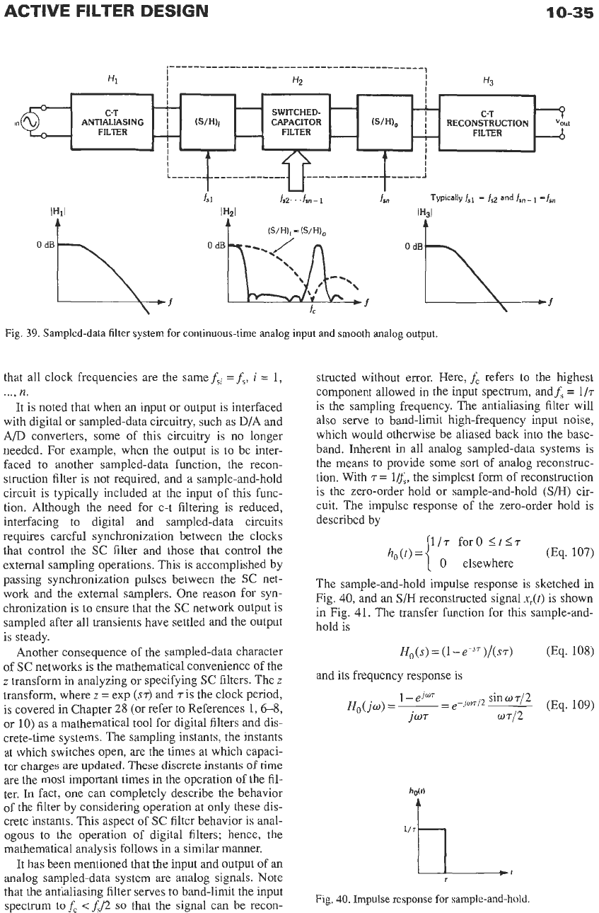
cuit. The impulse response of the zero-order hold is
described by
I/r
for0
<t<r
0
elsewhere
(Eq.
107)
h0
(t)
=
The sample-and-hold impulse response is sketched
in
Fig.
40,
and an
S/H
reconstructed signal
x,(t)
is shown
in Fig.
41.
The transfer function for this sample-and-
hold is
Ho(s)
=
(I-e-")/(s5-)
(Eq.
108)
and its frequency response
is
Fig,
40.
Impulse response
for
sample-and-hold.
10-36
REFERENCE
DATA
FOR ENGINEERS
Fig.
41.
Reconstruction with sample-and-hold.
It
can be seen that
Ho(jw)
has the (sin
x)/x
magnitude
response shown in Fig. 42A and the phase characteris-
tic shown in Fig. 42B.
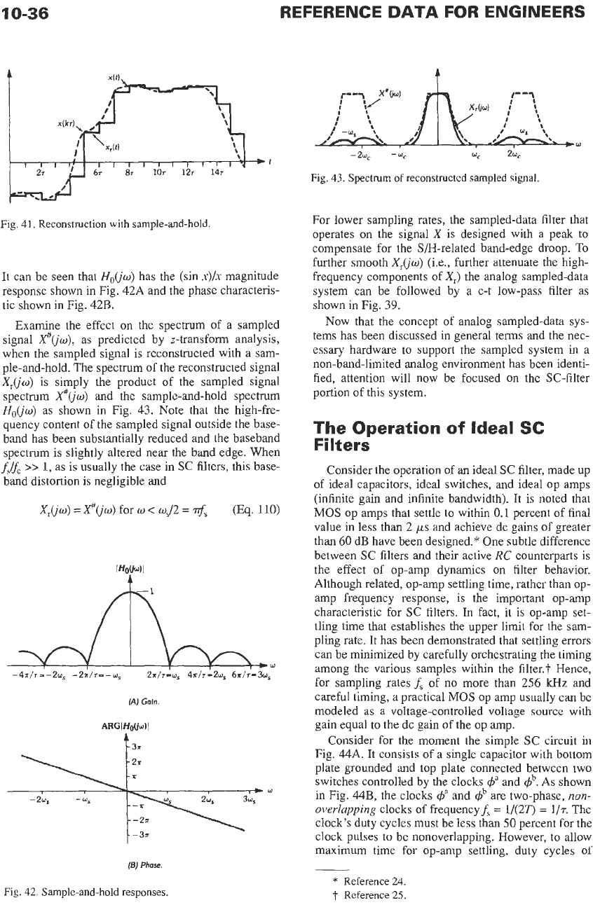
Examine the effect on the spectrum of a sampled
signal
pow),
as predicted by z-transform analysis,
when the sampled signal is reconstructed with a sam-
ple-and-hold. The spectrum of the reconstructed signal
X,(jw)
is simply the product of the sampled signal
spectrum
x#(jw)
and the sample-and-hold spectrum
Ho(jw)
as shown in Fig. 43. Note that
the
high-fre-
quency content of the sampled signal outside the base-
band has been substantially reduced and the baseband
spectrum is slightly altered near the band edge. When
&lf,
>>
1,
as is usually the case in SC filters, this base-
band distortion is negligible and
X,(jo)
=
x#(jw)
for
w
<
wJ2
=
..f,
(Eq.
110)
(A)
Gain
\
t:
-2w,
-us
(6)
Phase.
Fig. 42. Sample-and-hold responses.
-20,
-wc
wc
2%
Fig. 43. Spectrum
of
reconstructed sampled signal.
For lower sampling rates, the sampled-data filter that
operates on the signal
X
is designed with a peak to
compensate for the S/H-related band-edge
droop.
To
further smooth
X,(jw)
(i.e., further attenuate the high-
frequency components of
X,)
the analog sampled-data
system can be followed by a c-t low-pass filter as
shown in Fig. 39.
Now that the concept of analog sampled-data sys-
tems has been discussed in general terms and the nec-
essary hardware to support the sampled system in a
non-band-limited analog environment has been identi-
fied, attention will now be focused on the SC-filter
portion of
this
system.
The
Operation
of
Ideal
SC
Filters
Consider the operation of an ideal
SC
filter, made up
of
ideal capacitors, ideal switches, and ideal op amps
(infinite gain and infinite bandwidth). It is noted that
MOS
op amps that settle
to
within
0.1
percent of final
value in less than
2
ps
and achieve dc gains of greater
than
60
dB have been designed.* One subtle difference
between
SC
filters and their active
RC
counterparts is
the effect of op-amp dynamics on filter behavior.
Although related, op-amp settling time, rather than op-
amp frequency response, is the important op-amp
characteristic for
SC
filters.
In
fact, it is op-amp set-
tling time that establishes the upper limit for the sam-
pling rate. It has been demonstrated that settling errors
can be minimized by carefully orchestrating the timing
among the various samples within the filter.? Hence,
for sampling rates
f,
of no more than
256
kHz
and
careful timing, a practical
MOS
op
amp usually can be
modeled as a voltage-controlled voltage source with
gain equal
to
the dc gain of the op amp.
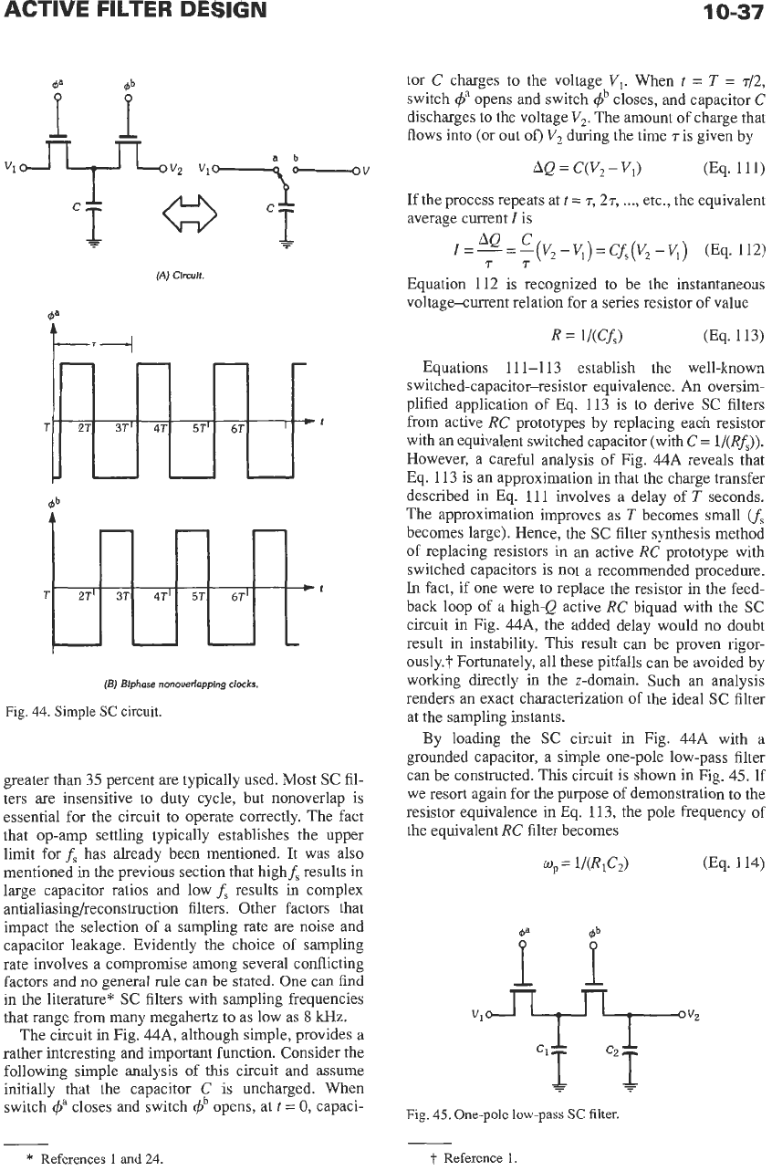
Consider for the moment the simple
SC
circuit
in
Fig. 44A. It consists of a single capacitor with bottom
plate grounded and top plate connected between two
switches controlled by
the
clocks
+a
and
+b.
As shown
in Fig. 44B, the clocks
+a
and
+b
are
two-phase,
non-
overlapping
clocks of frequency&
=
1/(2T)
=
117.
The
clock's duty cycles must be less than
50
percent for the
clock pulses to be nonoverlapping. However,
to
allow
maximum time for op-amp settling, duty cycles of
*
Reference 24.
t
Reference 25.
ACTIVE
FILTER
DESIGN
T
10-37
-
-
-
23'
3T
47'
5T
67'
+l
---
(A)
CIrcuL.
(5)
Blphase nonouerlapping clocks.
Fig.
44.
Simple
SC
circuit.
greater than
35
percent
are
typically used. Most SC fil-
ters are insensitive to duty cycle, but nonoverlap
is
essential for the circuit to operate correctly. The fact
that op-amp settling typically establishes the upper
limit forf, has already been mentioned. It was also
mentioned in the previous section that highf, results in
large capacitor ratios and low
f,
results in complex
antialiasing/reconstction
filters. Other factors that
impact the selection of a sampling rate are noise and
capacitor leakage. Evidently the choice of sampling
rate involves a compromise among several conflicting
factors and no general rule can be stated. One can find
in the literature" SC filters with sampling frequencies
that range from many megahertz to as low as
8
kHz.
The circuit
in
Fig. 44A, although simple, provides a
rather interesting and important function. Consider the
following simple analysis of
this
circuit and assume
initially that the capacitor
C
is uncharged. When
switch
+a
closes and switch
+b
opens, at
t
=
0,
capaci-
tor
C
charges to the voltage
V,.
When
t
=
T
=
r/2,
switch
4a
opens and switch
4b
closes, and capacitor
C
discharges to the voltage
V,.
The amount of charge that
flows into (or
out
of)
V,
during the time
r
is given by
AQ
=
C(Vz
-
VI)
(Eq.
11
1)
If the process repeats at
t
=
T,
27,
...,
etc., the equivalent
average current
I
is
AQ
C
I=-=-(V2
rr
-V,)=Cfs(V2
-V,)
(Eq. 112)
Equation 112
is
recognized to be the instantaneous
voltage-cunrent relation for a series resistor of value
R
=
MCfJ
(Eq. 113)
Equations
11
1-1
13 establish the well-known
switched-capacitor-resistor equivalence. An oversim-
plified application of Eq. 113 is to derive SC filters
from active
RC
prototypes by replacing each resistor
with
an
equivalent switched capacitor (with
C
=
l/(Rf,)).
However, a careful analysis of Fig. 44A reveals that
Eq. 113 is an approximation in that the charge transfer
described in Eq.
111
involves a delay of
T
seconds.
The approximation improves as
T
becomes small
(f,
becomes large). Hence, the
SC
filter synthesis method
of replacing resistors
in
an active
RC
prototype with
switched capacitors is not a recommended procedure.
In
fact, if one were to replace the resistor in the feed-
back loop of a high-Q active
RC
biquad with the SC
circuit
in
Fig. 44A, the added delay would no doubt
result in instability. This result can be proven rigor-
ously.? Fortunately, all these pitfalls can be avoided by
working directly in the z-domain. Such an analysis
renders an exact characterization of the ideal
SC
filter
at the sampling instants.
By loading the SC circuit in Fig. 44A with a
grounded capacitor, a simple one-pole low-pass filter
can be constructed.
This
circuit is shown in Fig.
45.
If
we resort again for the purpose of demonstration to the
resistor equivalence in Eq.
113,
the pole frequency of
the equivalent
RC
filter becomes
Fig.
45.
One-pole low-pass
SC
filter.
*
References
1
and
24.
t
Reference
1.
10-38
REFERENCE
DATA
FOR ENGINEERS
Substituting the SC equivalent for resistor
R,
in Eq.
114
yields the pole frequency for the SC filter, i.e.,
wp
=f,(C,/C,)
forf,
>>
2rfP
(Eq. 115)
Equation 115 provides much of the motivation for
SC filters. From Eq. 115, the inherent accuracy of the
SC implementation is seen immediately:
wp
no longer
depends
on
the
product
of
the components
R
and
C,
but on the clock,&, and the
ratio
of
two
Cs.
It was
mentioned previously that MOS capacitor ratios can
be held to tight tolerances and
f,
is derived from a very
precise crystal-controlled master clock.
In
addition,
note that the capacitor ratio
CJC,
equalsf,/wp., That is,
for constant
up,
C,/C,
scales in direct proporhon to&.
As
a consequence, the silicon area required to realize
the SC filter in Fig. 44 (for a fixed
wp
and minimum
capacitance
C,)
scales with
&.
For IC realizations,
minimum capacitors on the order of 1 pF are typically
used.
SC
Integrators
Most practical SC filters are realized with one op
amp per pole (and zero), and they use SC integrators
as
basic building blocks. Moreover, SC filters imple-
mented in this manner can be made insensitive to the
unavoidable parasitic capacitances that occur in an IC
realization and can, therefore, be implemented with
minimum-size capacitors.
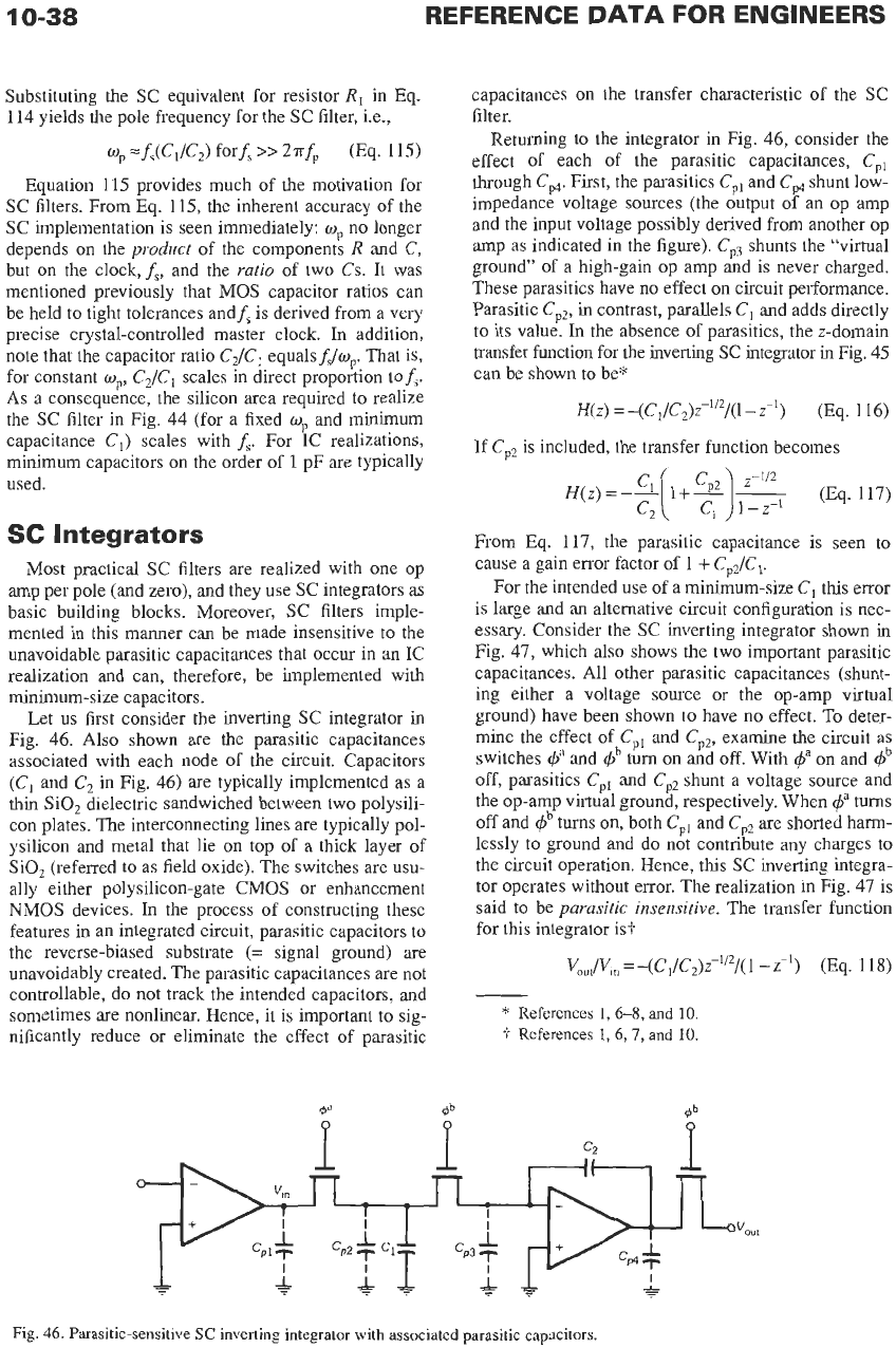
Let
us
first consider the inverting SC integrator
in
Fig. 46. Also shown are the parasitic capacitances
associated with each node of the circuit. Capacitors
(C,
and
C,
in Fig. 46) are typically implemented as a
thin SiO, dielectric sandwiched between two polysili-
con plates. The interconnecting lines are typically pol-
ysilicon and metal that lie on top
of
a thick layer of
SiO, (referred to as field oxide). The switches are
usu-
ally either polysilicon-gate CMOS or enhancement
NMOS devices.
In
the process of constructing these
features in an integrated circuit, parasitic capacitors to
the reverse-biased substrate
(=
signal ground) are
unavoidably created. The parasitic capacitances are not
controllable, do not track the intended capacitors, and
sometimes are nonlinear. Hence, it is important to sig-
nificantly reduce or eliminate the effect of parasitic
capacitances on the transfer characteristic of the SC
filter.
Returning to the integrator in Fig. 46, consider the
effect of each
of
the parasitic capacitances,
Cp,
through
Cp4.
First, the parasitics
Cpl
and
Cp4
shunt low-
impedance voltage sources (the output of an op amp
and the input voltage possibly derived from another op
amp as indicated in the figure).
Cp3
shunts the “virtual
ground”
of a high-gain op amp and is never charged.
These parasitics have
no
effect
on
circuit performance.
Parasitic
Cpz,
in contrast, parallels
C,
and adds directly
to its value.
In
the absence
of
parasitics, the z-domain
transfer function for the inverting SC integrator in Fig. 45
can be shown to be*
H(z)
=
-(c,/cz)z-1’2/(l
-
z-I)
(Eq.
116)
If
Cp2
is included, the transfer function becomes
H(z)=-C‘b+s)-
z-1/2
(Eq. 117)
e,
c,
1-z-’
1
0
1
I
I
I
I
From Eq. 117, the parasitic capacitance is seen to
cause a gain error factor of 1
+
Cp2/C,.
For the intended use
of
a minimum-size
C,
this error
is large and an alternative circuit configuration is nec-
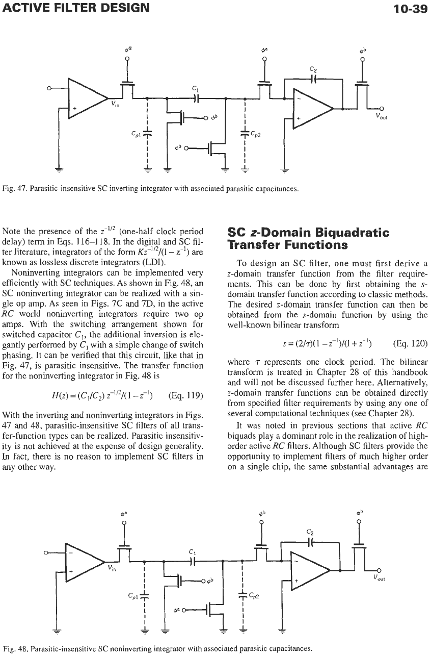
essary. Consider the SC inverting integrator shown
in
Fig. 47, which also shows the two important parasitic
capacitances. All other parasitic capacitances (shunt-
ing either a voltage source or the op-amp virtual
ground) have been shown to have no effect.
To
deter-
mine the effect of
C,,
and
Cp2,
examine the circuit as
switches and
4b
turn on and
off.
With
@
on
and
+b
off, parasitics
Cpl
and
Cp2
shunt a voltage source and
the op-amp virtual ground, respectively. When
turns
off and
$b
turns
on,
both
Cpl
and
Cp2
are shorted harm-
lessly to ground and do not contribute any charges to
the circuit operation. Hence, this SC inverting integra-
tor operates without error. The realization in Fig. 47 is
said to be
parasitic insensitive.
The transfer function
for this integrator is?
V,,,/V,,
=
-(C~/Cz)z-l’z/( 1
-
z-’)
(Eq.
1
18)
*
References
1,643,
and
10.
t
References
1,6,7,
and
10.
0
VO”
t
P
-0VO”t
Fig.
46.
Parasitic-sensitive
SC
inverting integrator with associated parasitic capacitors.
ACTIVE FILTER DESIGN
10-39
Fig.
47.
Parasitic-insensitive
SC
inverting integrator with associated parasitic capacitances
Note
the
presence of the z? (one-half clock period
delay) term
in
Eqs.
116-1
18.
In
the
digital and
SC
fil-
ter literature, integrators of the form Kz-'"/(l-
z-')
are
known as lossless discrete integrators
(LDI).
Noninverting integrators can be implemented very
efficiently with SC techniques. As shown in Fig.
48,
an
SC
noninverting integrator can be realized with a
sin-
gle op amp. As seen in Figs. 7C and 7D, in the active
RC
world noninverting integrators require two op
amps. With the switching arrangement shown for
switched capacitor
C,,
the additional inversion is ele-
gantly performed by
C,
with a simple change
of
switch
phasing. It can be verified that this circuit, like that in
Fig. 47, is parasitic insensitive. The transfer function
for the noninverting integrator in Fig.
48
is
H(z)
=
(C,/C,)
z-'"/(
1
-
z-') (Eq.
119)
With the inverting and noninverting integrators in Figs.
47 and 48, parasitic-insensitive
SC
filters of all trans-
fer-function types can be realized. Parasitic insensitiv-
ity is not achieved at the expense of design generality.
In
fact, there is
no
reason to implement
SC
filters in
any other way.
SC
z-Domain Biquadratic
Transfer Functions
To
design an SC filter, one must first derive a
z-domain transfer function from the filter require-
ments. This can be done by first obtaining the
s-
domain transfer function according
to
classic methods.
The desired z-domain transfer function can then be
obtained from the s-domain function by using the
well-known bilinear transform
s
=
(2/7)(
1
-
z-l)/(l
+
z-I) (Eq.
120)
where
r
represents one clock period. The bilinear
transform is treated in Chapter
28
of
this
handbook
and will not be discussed further here. Alternatively,
z-domain transfer functions can be obtained directly
from specified filter requirements by using any one of
several computational techniques (see Chapter
28).
It was noted in previous sections that active
RC
biquads play a dominant role
in
the realization of high-
order active
RC
filters. Although
SC
filters provide the
opportunity to implement filters of much higher order
on
a single chip, the same substantial advantages are
P
I
CPl
I
I
I
I
+
P
P
T
i
"in
I
I
I
I
","I
Fig.
48.
Parasitic-insensitive
SC
noninverting integrator
with
associated
parasitic capacitances.