Middleton W.M. (ed.) Reference Data for Engineers: Radio, Electronics, Computer and Communications
Подождите немного. Документ загружается.

21
-26
REFERENCE
DATA
FOR ENGINEERS
scintillating material, typically thallium-activated NaI
crystals, photomultipliers are extensively used to detect
the single flashes of light generated by the scintillating
material on bombardment by a single triggering parti-
cle, typically
X
rays or
a
gamma ray from a nuclear
disintegration process. If the scintillating material gene-
rates an average of
N
photons per disintegration incident
on
the effective photocathode of peak quantum efficien-
cy,
Y,,,,
the resultant average charge pulse, QA,
appearing in the anode circuit (disregarding all photons
or electrons producing no output charge) will be given
by the equation
QA
=
NY,,,aGe
where
a
is a spectral matching factor describing the
relative match between the scintillator spectral output
and cathode sensitivity.
Because of the random statistical fluctuations of
cathode quantum efficiency
Y,,,
and electron-multi-
plier gain
G,
as well as in the number of effective
photons,
N,
generated by the scintillator, the anode
charge, QA, will vary in magnitude from pulse to pulse,
introducing ambiguity in the determination of the
average magnitude of
N,
which in turn is used to
determine the energy of the triggering input particle, for
example the gamma ray. The ratio of the spread of the
amplitude of individually observed values of charge QA
at half maximum to the most probable value
QA(,,,,,)
is
called the “energy resolution” of the photomultiplier-
plus-scintillator combination and is commonly
7-
10%
minimum (see Fig.
23).
RESOLlJT[ON
=-\QA’QAlmari
ZE
OlLI
CHARGE MAGNITUDE
Qa
Fig.
23.
Energy
resolution
of
photomultiplier.
If
the input flux has no time-coherent groups of
photons, as it does in scintillation detection, photoelec-
trons are emitted singly at random emission times from
the photocathode and also generate an average output
charge,
QA,
given by
QA
=
Gq
where all photons or electrons generating
no
output
pulse are disregarded in measuring
G
and computing
QA. Assuming sufficiently large gain
G
and sufficiently
low generation of dark pulses
of similar charge ampli-
tude, the individual anode pulses of charge amplitude
Gq
can be detected and counted individually,
the
photomultiplier then acting as a single-electron counter.
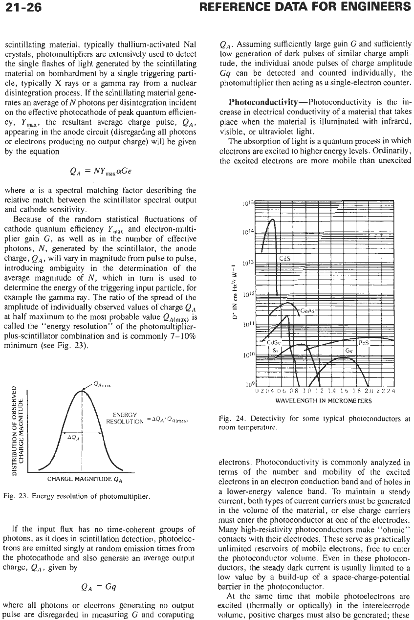
Photoconductivity-Photoconductivity is the in-
crease in electrical conductivity of a material that takes
place when the material is illuminated with infrared,
visible, or ultraviolet light.
The absorption of light is a quantum process in which
electrons are excited to higher energy levels. Ordinarily,
the excited electrons are more mobile than unexcited
10’4
1013
I
3
9
2
z
n
5
10’2
1011
1010
109
020406
08
10
12
14 16
18
202224
WAVELENGTH
IN
MICROMETERS
Fig. 24. Detectivity for some
typical
photoconductors
at
room temperature.
electrons. Photoconductivity is commonly analyzed in
terms of the number and mobility
of
the excited
electrons in an electron conduction band and of holes
in
a lower-energy valence band.
To
maintain a steady
current, both types
of
current carriers must be generated
in the volume of the material, or else charge carriers
must enter the photoconductor at one of the electrodes.
Many high-resistivity photoconductors make “ohmic”
contacts with their electrodes. These serve as practically
unlimited reservoirs
of
mobile electrons, free to enter
the photoconductor volume. Even in these photocon-
ductors, the steady dark current
is
usually limited to a
low value by a build-up
of
a space-charge-potential
barrier in the photoconductor.
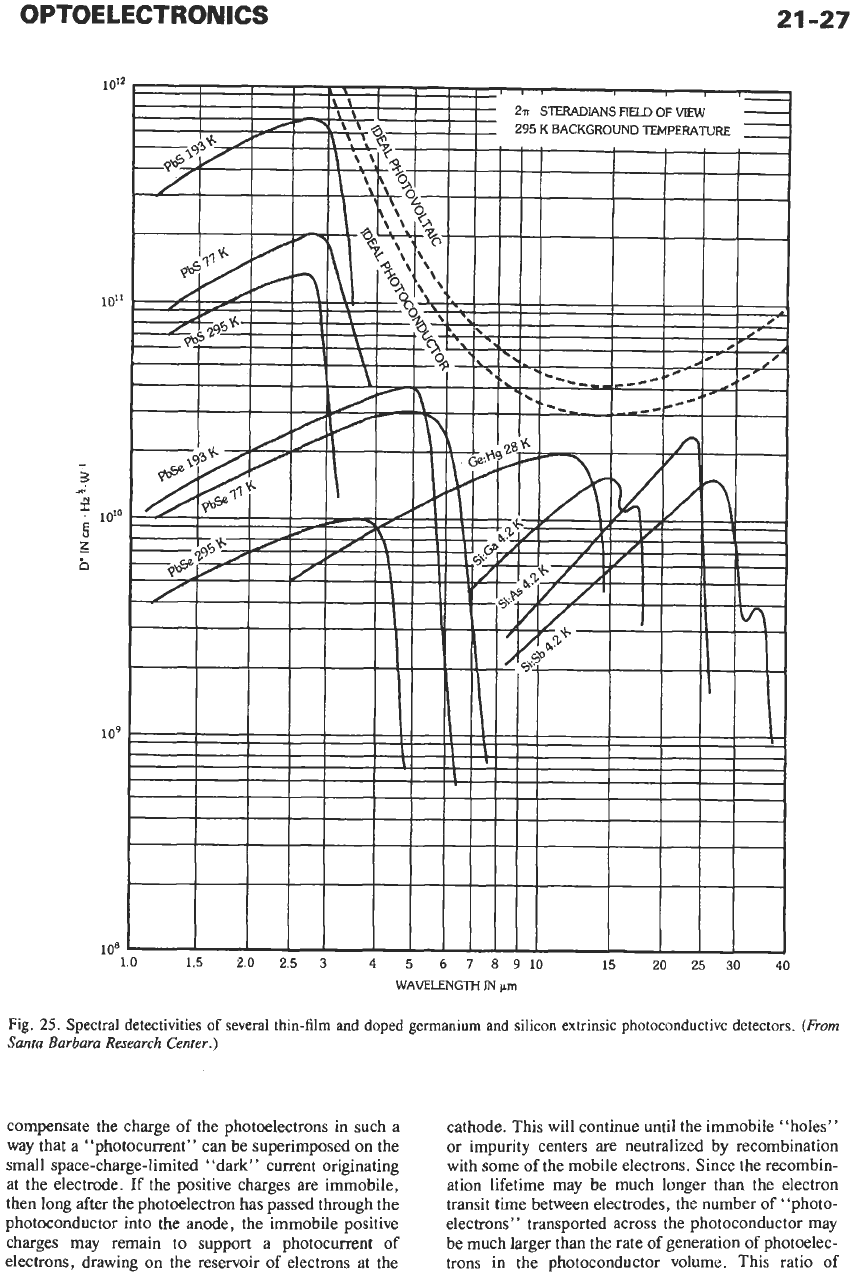
At the same time that mobile photoelectrons are
excited (thermally or optically) in the interelectrode
volume, positive charges must also be generated; these
OPTOELECTRONICS
1
o’*
io9
108
21
-27
15 20 25
30
40
1.0
1.5
2.0
2.5
3
4
5
6
7
8
9
10
WAVELENGTH
IN
pm
Fig.
25.
Spectral detectivities
of
several thin-film and doped germanium and silicon extrinsic photoconductive detectors.
(From
Santa
Barbara
Research
Center.)
compensate the charge of the photoelectrons in such a
way that a “photocurrent” can be superimposed
on
the
small space-charge-limited “dark” current originating
at the electrode.
If
the positive charges are immobile,
then
long
after the photoelectron has passed through the
photoconductor into the anode, the immobile positive
charges may remain to support a photocurrent
of
electrons, drawing
on
the reservoir of electrons at the
cathode. This will continue until the immobile “holes”
or impurity centers are neutralized by recombination
with some
of
the mobile electrons. Since the recombin-
ation lifetime may be much longer than the electron
transit time between electrodes, the number
of
“photo-
electrons” transported across the photoconductor may
be much larger than the rate
of
generation
of
photoelec-
trons
in the photoconductor volume. This ratio of
21-28
REFERENCE
DATA
FOR ENGINEERS
photocurrent to generation rate is called the photocon-
ductive gain.
The photoconductive gain of a pure material can
often be greatly increased by addition of localized traps
lying near the conducting band. Since these are in
thermal equilibrium with the conducting band, they
serve as an additional reservoir of the charge carriers.
This can increase both the response time and the
sensitivity by a large factor.
Practically all materials are photoconductors in the
sense that light of the correct wavelengths will generate
current carriers. However, in many materials the photo-
conductivity is not detectable by ordinary measure-
ments, either because of very short carrier lifetimes or
because of a large dark current. The useful photocon-
ductors, characterized by comparatively long lifetimes
and low dark currents, have most of their charge carriers
immobile (in the dark). Light of the proper energy can
excite these carriers through the forbidden energy
regions into the conduction bands. The long-wavelength
limit of photoconductivity at low temperatures is given
approximately by
A,,,
=
hc/E,
where,
E,
is the forbidden band gap,
h
is Planck’s constant,
c
is the velocity of light.
For wavelengths longer than
5
micrometers, this equa-
tion gives a band gap smaller than
‘/4
electronvolt.
Photoconductors with such small energy gaps are
usually cooled to reduce the dark conductivity due to
thermal excitation of carriers across the gap.
Values
of
D*,
a commonly used figure of merit for
photoconductors, for several typical photoconductors at
room temperature are shown in Fig.
24.
The photocon-
ductors with long-wavelength cutoffs will be considera-
bly more sensitive if they are cooled below room
temperature.
Photodiodest-When photons irradiate a semicon-
ductor having a band gap less than the energy of the
photons, hole-electron pairs are produced. By forming
a pn junction
in
a semiconductor, those hole-electron
pairs can be collected. The resulting photodiode may
have a quantum efficiency (ratio of collected photoelec-
trons to impinging photons) of from
0.2
to
0.7
or higher
with antireflection coating.
Photodiodes have two primary operating modes, the
photovoltaic mode and the reverse-biased mode that is
often referred to incorrectly as the photoconductive
mode. In the photovoltaic mode, the unbiased junction
is illuminated to stimulate the production of hole-
?
Stillman,
G.
E.,
and
Wolfe,
C.
M.,
“AvalanchePhotodi-
odes,” in
Semiconductor and Semimetals,
Vol.
12
(New
York:
Academic Press,
Inc.,
1977;
pp. 291-393).
electron pairs. Charge separation then occurs in the
field of the junction, and a current and/or voltage
results. Since photovoltaic cells produce a short-circuit
photocurrent that is linear with respect
to
the radiation
incident upon the pn junction, they are well suited for
low-level light detection and measurement. This is
especially true for narrow-band-gap materials and de-
vices where the leakage current of reverse-biased diodes
is often high enough to contribute undesirable noise.
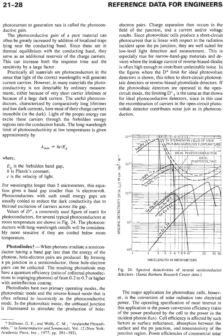
In
the figures where the
D*
limit for ideal photovoltaic
detectors is shown, this refers to short-circuit photovol-
taic detectors or reverse-biased photodiode detectors. If
the photovoltaic detectors are operated in the open-
circuit mode, the limiting
D**
is the same as that shown
for ideal photoconductive detectors, since in this case
the recombination of carriers in the open-circuit photo-
voltaic detector contributes noise
just
as in photocon-
duction.
10“
1
I
i
i
i
iiii
I I
2a
STERADIANS FIELD
OF
VIEW
295
K
BACKGROUND TEMPERATURE
c
k
2
8
2
109
u.
8
F-
a
v,
108
1
2
3
4
5
678910
20
30
40
WAVELENGTH IN MICROMETERS
10’’
10“’
I I
,
I
VI
IYI
I II
Fig.
26. Spectral detectivities
of
several semiconductor
detectors.
(Santa Barbara Research Center data.)
The major application for photovoltaic cells, howev-
er, is the conversion of solar radiation into electrical
power. The operating specification of most interest in
this application
is
the power conversion efficiency (ratio
of
the power produced by the cell to the power in the
incident photon flux). Cell efficiency is affected by such
factors as surface reflectance, absorption between the
surface and the pn junction, and transmissivity of the
junction region. Power efficiencies
of
commercial solar
OPTOELECTRONICS
21-29
0.5
1
5
10
20
WAVELENGTH
IN
MICROMETERS
Fig.
27.
Spectral response
of
detectors.
cells range from
5%
to
a
maximum of about
15%.
The
best developed solar-cell material is silicon,
but
consid-
erable work has been expended
on
gallium arsenide,
indium phosphide, and cadmium sulfide. Fabrication
advances now permit the production
of
long
silicon
ribbons, and this should eventually result in significant
cost reductions for silicon solar-energy converters.
In
the photoconductive mode, a photodiode (usually
of
special construction) is reverse biased and exposed to
optical radiation.,The resulting hole-electron pairs sep-
arate at the junction and establish a current that consists
of a small and constant reverse leakage (the dark
current) and the photocurrent (the signal). The photo-
current is linear with respect to the incident radiation.
The dark current establishes a minimum noise level
below which operation is impractical.
An
important
advantage of photoconductive operation over the photo-
voltaic mode is response time.
A
photodiode resembles
a parallel-plate capacitor. Unbiased operation is slowed
by high junction capacitance, whereas reverse-biased
operation reduces junction capacitance and enhances
response time.
21
-30
REFERENCE
DATA
FOR ENGINEERS
1.0
1.5
2.0
2.5
3
4
5
6
7
8
9
10
15
20
25
30
40
WAWLENGHTS
IN MICROMETERS
Fig.
28.
Spectral response
of
detectors.
A photodiode of major importance is the avalanche
photodiode. This device is a modified photodiode
biased just below the avalanche breakdown region.
Photons impinging upon the junction region create
hole-electron pairs that initiate an avalanche multiplica-
tion of carriers across the junction. The resulting
internal gain and response time make avalanche photo-
diodes suitable for operation in wide-bandwidth appli-
cations, where the
s/n
ratio is limited by the thermal
noise of the load resistor and amplifier noise
of
wide-
bandwidth amplifiers, formerly reserved for the photo-
multiplier tube.
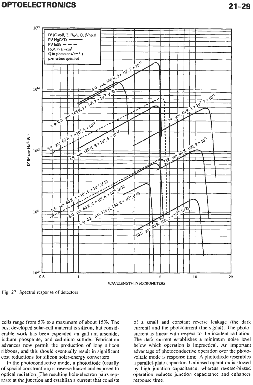
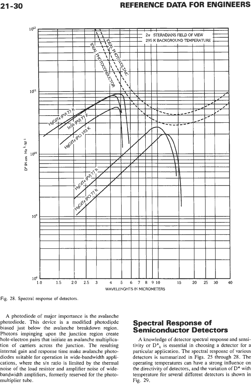
Spectral Response
of
Semiconductor Detectors
A
knowledge of detector spectral response and sensi-
tivity or
D**
is essential in choosing a detector for a
particular application. The spectral response of various
detectors is summarized in Figs.
25
through
28.
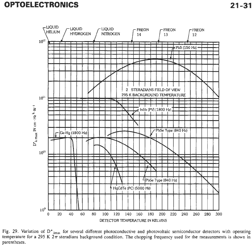
The
operating temperatures can have a strong influence
on
the directivity of detectors, and the variation of
D*
with
temperature for several different detectors is shown in
Fig.
29.
OPTOELECTRONICS
21-31
DETECTOR
TEMPERATURE
IN
KELVINS
Fig.
29.
Variation of
D*Amar
for
several different photoconductive and photovoltaic semiconductor detectors with operating
temperature for a
295
K
2~
steradians background condition. The chopping frequency used
for
the measurements
is
shown
in
parentheses.
22
Optical
Communications
Chester
S.
Gardner and George Papen
Optical Detectors and Noise
22-2
Modulation Techniques
22-3
Pulse-Position Modulation
Binary Orthogonal Signaling
Optical Transmitters
22-5
Incoherent Sources
Coherent Sources
Optical Receivers
22-8
Direct-Detection Receivers
Heterodyne-Detection Receivers
Background Radiation
22-12
Atmospheric Effects
22-13
Absorption
Scattering
Turbulence
Fiber Waveguide Transmission
22-19
Terminology
Losses
Dispersion
Fiber Bandwidth
Splicing
Connectors
Sample Calculation
22-
1
22-2
REFERENCE DATA FOR ENGINEERS
In
recent years, advances in device technology have
significantly enhanced the capabilities
of
optical com-
munication systems. High-data-rate systems have been
constructed for space applications, and fiber-optic
systems are finding wide use in telephone and
data communications.
In
this chapter, the design of
both fiber and free-space optical communication sys-
tems
is
discussed. Systems aspects are emphasized in
this chapter. More detailed information
on
device
technology can be found in Chapter
21
on Optoelec-
tronics.
OPTICAL DETECTORS AND
NOISE
Optical detectors can be classified into two general
categories. Photomultiplier tubes (PMT) and vacuum
photodiodes are photoemissive devices that emit elec-
trons into a vacuum or gas. Avalanche photodiodes
(APD). pin photodetectors, and phototransistors are
solid-state devices in which the excited charge is
transported in the solid by holes and electrons. Pho-
tomultiplier tubes, APDs, and pin photodetectors
are the most widely used in optical communication
systems.
Photomultiplier tubes are typically used when high
sensitivity and bandwidth are required. Because their
internal gain can be as high as
IO7,
the output signal
level is large compared to the thermal noise
of
the
succeeding amplifiers. Receivers employing PMTs are,
therefore, shot-noise limited. The disadvantages of
PMTs are that they are relatively bulky and fragile
compared to solid-state detectors and they require
high-voltage power supplies. Solid-state detectors are
small, reliable, and inexpensive, and they exhibit high
quantum efficiency through the visible to near-infrared
portions of the spectrum. Avalanche photodiodes are
characterized by high gain and bandwidth.
Optical detectors are square-law devices because they
respond to intensity rather than amplitude. The detec-
tion process involves the interaction of incident photons
with the detector material.
In
the case of vacuum
photodiodes and PMTs, the incident photons generate
photoelectrons that are ejected from the photocathode
and flow to the anode. Electron-hole pairs are created in
the lattice structure
of
solid-state detectors by the
incident photons. The quantum efficiency
(7)
of
a
detector is the fraction
of
incident photons that produce
a photoelectron or electron-hole pair. The quantum
efficiencies
of
photocathodes
in
PMTs range from a few
tenths of a percent to about
30
percent. Silicon photo-
detectors can have quantum efficiencies exceeding
80
percent.
In
either case, each detected photon causes an
impulse of current to flow in the detector load resistor.
The photocurrent is equal
to
the number of electrons
emitted per second times the electron charge
(e
=
1.6
X
C).
Photodetector efficiency is sometimes ex-
pressed in terms
of
responsivity, which is defined as the
photocurrent divided by the incident optical power.
Responsivity
(R)
can be written in terms
of
the detector
quantum efficiency, electron charge, and photon energy
(hf)
where,
h
is Planck’s constant
(6.63
X
f
is the optical frequency.
The detector output current can be modeled by using
J
*
s),
the following formula:
N(0
i(t)
=
Gjg(t
-
T~)
+
i~h(t)
(Eq.
2)
j=
1
where,
N(t)
=
number
of
photons that have been detected
during the time interval
(-00,
t),
T~
=
arrival time
of
the jth photon,
Gj
=
detector gain for the jth photon,
g(t)
=
detector impulse response,
iTh(t)
=
detector thermal noise current.
In
the above expression,
N
is a random process whose
statistics are related to the optical intensity.
If
the
intensity is deterministic,
N
is Poisson distributed
Prob
(N
=
k)
=
(pk/k!)e-’
(Eq.
3)
where,
P(t)
is the optical power.
The expected value and variance of
N
equal
p.
E(N)
=
Var(N)
=
(r]/hf)
P(T)
d~
(Eq.
5)
The internal amplification processes
of
PMTs and
APDs are noisy
so
that
G
is also random. This effect
introduces additional noise into the detection process.
Amplification noise is most significant in APDs and
should be considered in analyzing receiver perform-
ance. However, if the gain is assumed to be constant,
the mean and variance
of
the detector output current are
given by Campbell’s theorem
The first term on the right-hand side
of
Eq.
7
is called
shot noise. It is caused by the statistical nature
of
the
22-3
photon detection process. The term
dTh
is the thermal
noise variance, which is given by
where,
RL
=
detector load resistance,
k
=
Boltzmann’s constant,
TL
=
equivalent temperature of the detector load
resistor (kelvins),
B
=
detector bandwidth.
Typically, the detector bandwidth will be larger than or
equal
to
the bandwidth of
P(t).
In
this case, the
convolutions in
Eqs.
6
and
7
can be approximated by
g2(T)
dT
=
2e2BP(t)
(Eq.
10)
In
deriving Eqs.
9
and
10,
it
was assumed that
g(t)
is an
ideal low-pass filter, with bandwidth
B.
Consequently,
the mean and variance
of
the output current are given by
E[i(t)l
=
(veG/hf)
(P,
+
6)
(Eq.
11)
Var[i(r)l
=
(2ve2G2B/hf) (P,
+
Pb)
+
4kTLB/RL
0%.
12)
where,
P,
is the signal power,
Pb
is the optical background noise power.
For atmospheric systems operating during the daytime,
pb
can be quite large. For fiber systems,
Pb
is negligible.
Eq.
12
is valid for PMTs and detectors with
no
internal gain
(G
=
1).
For APDs, the random variation
of the internal gain must be considered when calculating
the variance of the output current. The details are
complicated and need not be repeated here. The vari-
ance of the output current for an APD is given by*
~ar[i(t)l
=
[2qe2~’~(~)~/hfl
(P,
+
pb)
+
4kTLBIRL
(Eq. 13)
where,
F(G)
=
pc
+
(2
-
l/G)(l
-
p),
0%.
14)
G
is the mean gain,
p
is the ratio
of
hole collision ionization
probability to electron collision ionization
probability.
*
Reference
1
For silicon APDs, pis between
0.02
and 0.03, and
G
is
typically less than
200.
For noise-free avalanche gain,
F(G)
would be equal to
1.
The current variance is proportional to the noise
power at the detector output. The signal power is
proportional to the square of the mean signal current.
Therefore, the signal-to-noise power ratio (SNR) at the
detector output is given by
Thermal-noise-limited detection occurs when the inter-
nal gain of the detector and the optical signal power are
low.
In
this case, thermal noise dominates the detection
process, and the SNR becomes
SNR
=
[(veG/hf)PS]*/(4kTLB/RL)
Thermal noise limited (Eq.
16)
If the internal gain of the detector is high
so
that
detection is shot-noise limited, the SNR can be written
as
SNR
=
(7$2h@)
[P2,/(P,
-t
Pb)]
Shot noise limited
(Eq.
17)
MODULATION TECHNIQUES
An
optical carrier can be modulated with any of the
conventional amplitude, phase, and frequency tech-
niques employed at radio frequencies. However, intensi-
ty modulation and polarization modulation are the most
widely used methods for optical systems.
In
digital
communications, the polarization state of the optical
carrier can be used to represent the value of a data bit.
Bits can be represented as either right or left circular
polarization or as any two orthogonal linear polarization
states. Lithium niobate (LiNb03) and lithium tantalate
(LiTaO,) are two of the more commonly used electro-
optic crystals for polarization modulators. Intensity
modulation can be used for analog and digital signals.
Analog signals are sometimes used to modulate RF
subcarriers by conventional phase or frequency modula-
tion. The optical intensity is then modulated by the RF
subcarrier. Intensity modulation can be accomplished
directly in laser diodes and LEDs by varying the diode
forward current. External acousto-optic and electro-
optic modulators can also be used to vary the optical
intensity continuously.
Pulse-Position Modulation
Pulse-position modulation (PPM) is a very effective
digital intensity-modulation technique. In
M-ary
PPM,
each time slot is divided into
M
equal intervals.
A
single
pulse
of
constant energy is transmitted during one of the
M
intervals. During a single time slot, one of
M