Middleton W.M. (ed.) Reference Data for Engineers: Radio, Electronics, Computer and Communications
Подождите немного. Документ загружается.

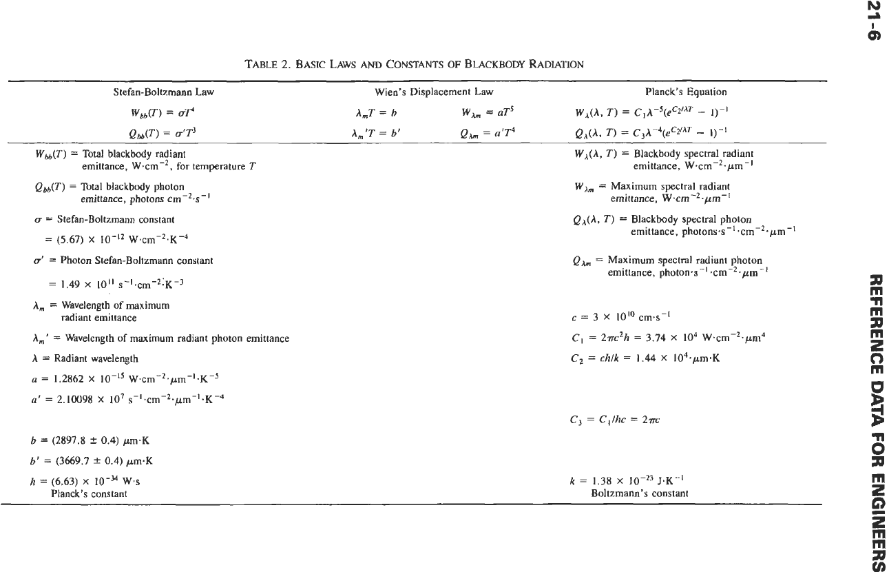
TABLE
2.
BASIC
LAWS
AND CONSTANTS
OF
BLACKBODY
RADIATION
Planck's Equation
Stefan-Boltzmann Law Wien's Displacement Law
wbb(T)
=
UT'
h,T
=
b
W,,,,
=
aT5
w,,(A,
T)
=
c,A-~(~c~/AT
-
I)-I
Qbb(T)
=
u'T3
A,'T
=
b'
QAm
=
a'T4
QA(h,
T)
=
~~~-~(e~2'~~
-
i)-1
Wn(A,
T)
=
Blackbody spectral radiant
emittance, W.cm-'.pm-'
wbb(T)
=
Total blackbody radiant
emittance, W.cm-',
for
temperature
T
Qbb(T)
=
Total blackbody photon
emittance, photons crn-'*s-I
u
=
Stefan-Boltzmann constant
=
(5.67)
X
IO-'*
WVX-'.K-~
WAm
=
Maximum spectral radiant
emittance,
Wan
-'
'firn
-I
Qh(A,
T)
=
Blackbody spectral photon
emittance, photons.
s
-
.cm
-'.
pm
u'
=
Photon Stefan-Boltzmann constant
QAm
=
Maximum spectral radiant photon
311
m
n
rn
311
0
m
0
P
311
rn
2
G)
rn
rn
XI
v)
emittance, phot0n.s
-I
an-2
'pm
-'
=
1.49
X
1011
s-l.cm-Z:K-3
A,,,
=
Wavelength
of
maximum
radiant emittance
A,
'
=
Wavelength of maximum radiant photon emittance
A
=
Radiant wavelength
o
=
1.2862
X
10-'5W.cm-2~pm-'.K-5
a'
=
2.10098
X
lo7
s-lm~-~.pm-'.K-~
c
=
3
x
1Olo
cm.s-'
C1
=
27rczh
=
3.74
X
lo4
W.cm-'.pm4
Cz
=
ch/k
=
1.44
X
104.pm.K
s
s
6
C3
=
Cllhc
=
~TC
b
=
(2897.8
5
0.4) pm.K
b'
=
(3669.7
2
0.4)
pm*K
h
=
(6.63)
X
W.s
k
=
1.38
x
J.K-~
Planck's constant Boltzmann's constant
E
OPTOELECTRONICS
21
-7
A
IN
MICROMETERS
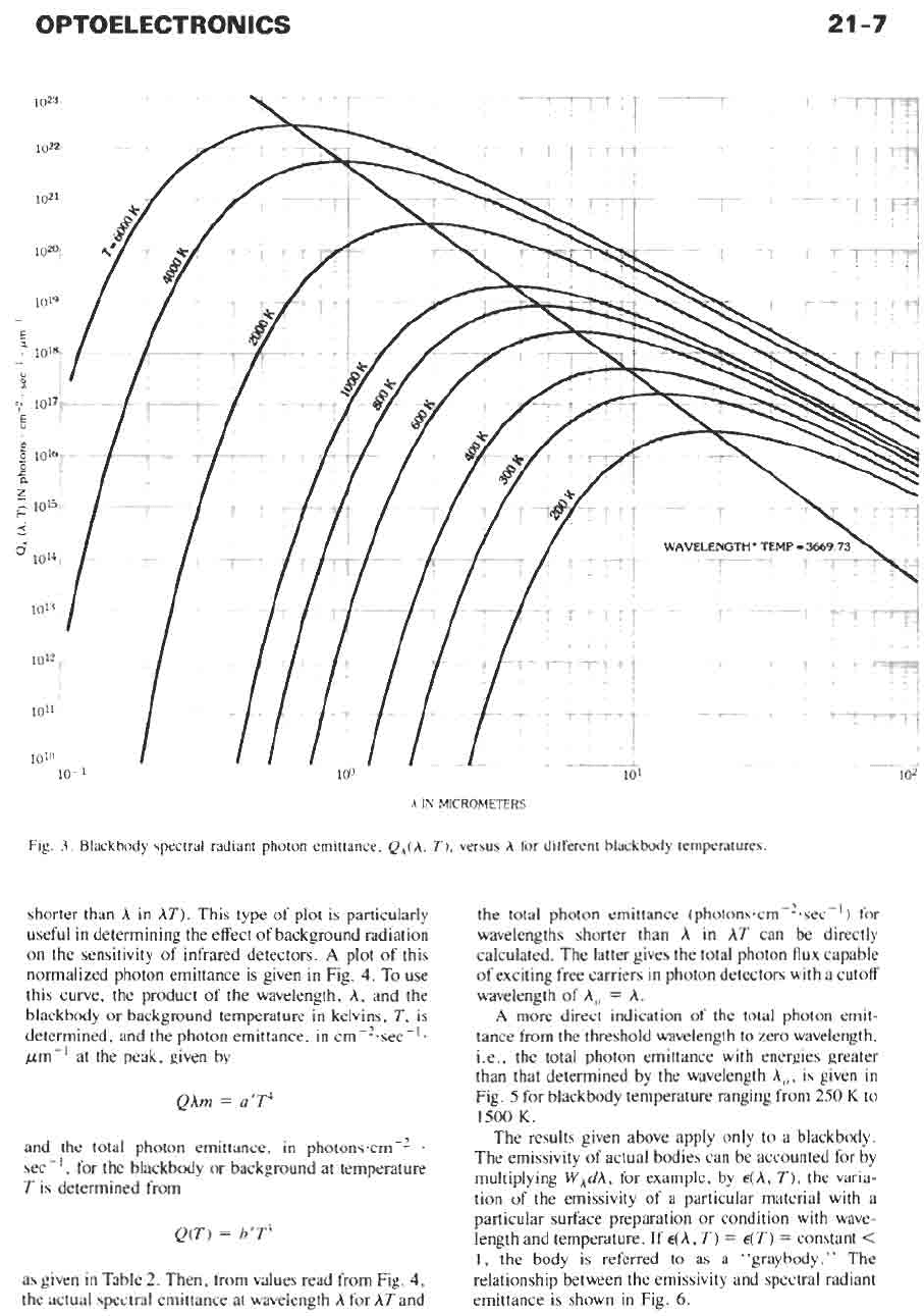
Fig.
3.
Blackbody spectral radiant photon emittance,
Qn(A,
T),
versus
A
for
different blackbody temperatures.
shorter than
A
in
AT).
This type of plot is particularly
useful in determining the effect of background radiation
on the sensitivity of infrared detectors.
A
plot of this
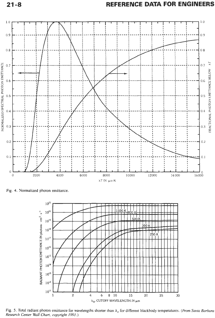
normalized photon emittance is given in Fig.
4.
To
use
this curve, the product of the wavelength,
A,
and the
blackbody
or
background temperature in kelvins,
T,
is
determined, and the photon emittance, in cm-2.sec-1*
pm-I at the peak, given by
QAm
=
a?
the total photon emittance (photons*cm-2.sec-l) for
wavelengths shorter than
A
in
AT
can
be
directly
calculated. The latter gives the total photon flux capable
of exciting free carriers in photon detectors with a cutoff
wavelength of
A,
=
A.
A
more direct indication of the total photon emit-
tance from the threshold wavelength to
zero
wavelength,
i.e., the total photon emittance with energies greater
than that determined by the wavelength
A,,
is given in
Fig.
5
for blackbody temperature ranging from
250
K
to
1500
K.
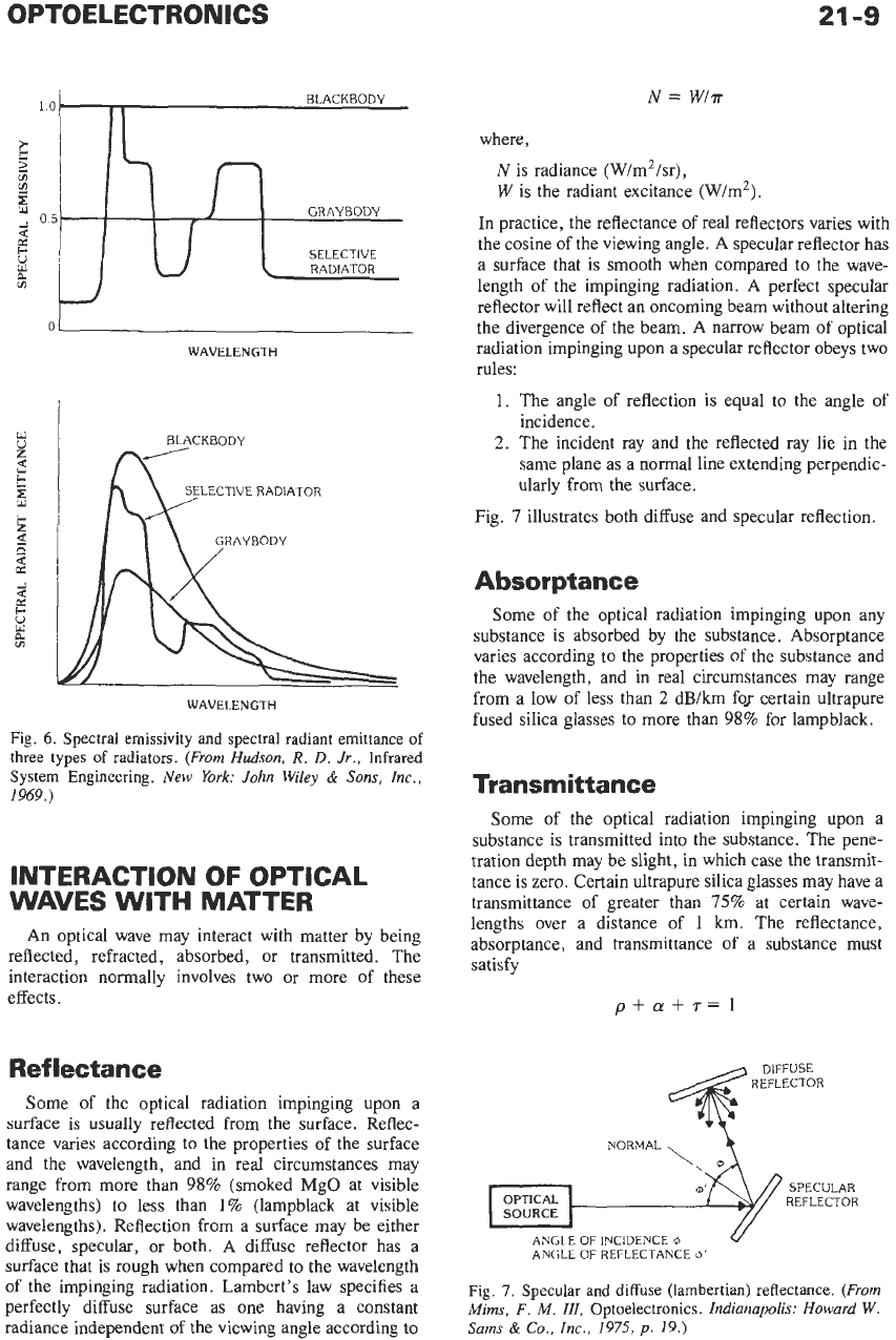
The results given above apply only to a blackbody.
The emissivity of actual bodies can
be
accounted
for
by
tion of the emissivity
of
a particular material with a
and the total photon emittance, in photons-cm-2
T
is determined from
sec-’’
for
the
Or
background
at
temperature
multiplying
WAdA,
for example, by
E(A,
T),
the varia-
particular surface preparation
or
condition with wave-
length and temperature. If
E(A,
T)
=
E(T)
=
constant
<
1,
the body is referred to as a “graybody.” The
relationship between the emissivity and spectral radiant
emittance is shown in Fig.
6.
Q(T)
=
b‘T3
as given in Table
2.
Then, from values read from Fig.
4,
the actual spectral emittance at wavelength
A
for
AT
and
21-8
REFERENCE
DATA
FOR ENGINEERS
0
2000
4000
6000
8000
10000
12000
14000 16000
AT
IN
pm.K
Fig.
4.
Normalized photon emittance.
*
N
Y)
0
c
Q
+.
6
f
B
Id'
Id0
1019
lo'*
10"
1
0l6
1015
1
014
1013
10'2
10"
15
20
25
30
1
2
4
6
810
A,,
CUTOFF
WAVELENGTH
IN
bm
Fig.
5.
Total radiant photon emittance for wavelengths shorter than
A,
for different blackbody temperatures.
(From Sum Barbara
Research Center
Wall
Chart, copyright
1991
.)
OPTOELECTRONICS
21
-9
BLACKBODY
1.0
II
WAVELENGTH
I
BLACKBODY
WAVELENGTH
Fig.
6.
Spectral emissivity
and
spectral
radiant
emittance
of
three
types
of
radiators.
(From Hudson,
R.
D.
Jr.,
Infrared
System
Engineering.
New
York:
John
Wiley
&
Sons, Inc.,
1969.)
INTERACTION
OF
OPTICAL
WAVES WITH MATTER
An optical wave may interact with matter by being
reflected, refracted, absorbed, or transmitted. The
interaction normally involves two or more of these
effects.
Reflectance
Some of the optical radiation impinging upon a
surface is usually reflected from the surface. Reflec-
tance varies according to the properties of the surface
and the wavelength, and in real circumstances may
range from more than
98%
(smoked MgO at visible
wavelengths) to less than
1%
(lampblack at visible
wavelengths). Reflection from a surface may be either
diffuse, specular,
or
both.
A
diffuse reflector has a
surface that is rough when compared to the wavelength
of
the impinging radiation. Lambert's law specifies a
perfectly diffuse surface as one having a constant
radiance independent of the viewing angle according to
N
=
Wlrr
where,
N
is radiance (W/m2/sr),
W
is
the radiant excitance (W/m2).
In practice, the reflectance
of
real reflectors varies with
the cosine of the viewing angle. A specular reflector has
a surface that is smooth when compared to the wave-
length of the impinging radiation.
A
perfect specular
reflector will reflect an oncoming beam without altering
the divergence
of
the beam. A narrow beam of optical
radiation impinging upon a specular reflector obeys two
rules:
1.
The angle of reflection is equal to the angle of
incidence.
2.
The incident ray and the reflected ray lie in the
same plane
as
a normal line extending perpendic-
ularly from the surface.
Fig.
7
illustrates both diffuse and specular reflection.
Absorptance
Some of the optical radiation impinging upon any
substance is absorbed by the substance. Absorptance
varies according
to
the properties of the substance and
the wavelength, and in real circumstances may range
from a low of less than
2
dB/km fox certain ultrapure
fused silica glasses to more than
98%
for lampblack.
Transmittance
Some of the optical radiation impinging upon a
substance is transmitted into the substance. The pene-
tration depth may be slight, in which case the transmit-
tance is zero, Certain ultrapure silica glasses may have a
transmittance of greater than
75%
at certain wave-
lengths over a distance of
1
km. The reflectance,
absorptance, and transmittance of a substance must
satisfy
p+
a+
7=
1
DIFFUSE
REFLECTOR
NORMAL
SPECULAR
REFLECTOR
OPTICAL
ANGLE
OF
INCIDENCE
d
ANGLE
OF
REFLECTANCE
0'
Fig.
7.
Specular
and
diffuse
(lambertian) reflectance.
(From
Mims,
F. M.
111,
Optoelectronics.
Indianapolis: Howard
W.
Sums
&
Co.,
Inc.,
1975,
p.
19.)
21-10
REFERENCE DATA FOR ENGINEERS
where,
p
is reflectance,
(Y
is absorptance,
7
is transmittance.
Refraction
A ray of optical radiation passing from one medium
to another is bent at the interface of the two mediums if
the angle of incidence is unequal to 90". The index of
refraction for a substance is the sine of the angle of
incidence divided by the sine of the angle
of
refraction.
Refractive index varies with wavelength and ranges from
1.002914 (air at
656
nm) to 2.7 (crystalline titanium
oxide).
OPTICAL SOURCES
Important optoelectronic sources are tungsten lamps,
fluorescent lamps, glow-discharge lamps, electrolumi-
nescent diodes, and lasers.
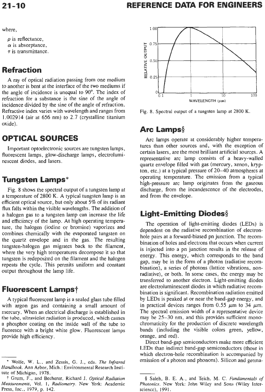
Tungsten Lamps*
Fig.
8
shows the spectral output of a tungsten lamp at
a temperature of 2800
K.
A typical tungsten lamp is an
efficient optical source, but only about
5%
of its radiant
flux falls within the visible wavelengths. The addition of
a halogen gas to a tungsten lamp can increase the life
and efficiency of the lamp. At high operating tempera-
ture, the halogen (iodine or bromine) vaporizes and
combines chemically with the evaporated tungsten on
the
quartz
envelope and in the gas. The resulting
tungsten-halogen gas migrates back to the filament,
where the very high temperatures decompose it
so
that
tungsten is redeposited on the filament and the halogen
repeats the cycle. This permits uniform and constant
output throughout the lamp life.
Fluorescent Lamps?
A typical fluorescent lamp is a sealed glass tube filled
with argon gas and containing a small amount of
mercury. When an electrical discharge is established in
the
tube,
ultraviolet radiation is produced, which causes
a phosphor coating on the inside wall of the tube to
fluoresce with a bright white glow. Fluorescent lamps
provide high efficiency.
-
*
Wolfe,
W.
L.,
and
Zessis,
G.
J.,
eds.
The Infrared
Handbook.
Ann Arbor, Mich.
:
Environmental Research Insti-
tute
of Michigan, 1978.
T
Grum,
F.,
and Becherer, Richard
J.
Optical Radiation
Measurements,
Vol.
1,
Radiometry.
New York: Academic
Press, Inc., 1979,
p.
142.
0.1
1
10
100
WAVELENGTH
(p)
Fig.
8.
Spectral output
of
a tungsten lamp at
2800
K.
Arc Lamps§
Arc lamps operate at considerably higher tempera-
tures than other sources and, with the exception of
certain lasers, are the most brilliant artificial sources.
A
representative arc lamp consists of a heavy-walled
quartz envelope filled with gas (mercury, xenon, kryp-
ton, etc.) at a typical pressure of 20-40 atmospheres at
operating temperature. The emission from a typical
high-pressure arc lamp originates from the gaseous
discharge, from the incandescence of the electrodes,
and from the envelope.
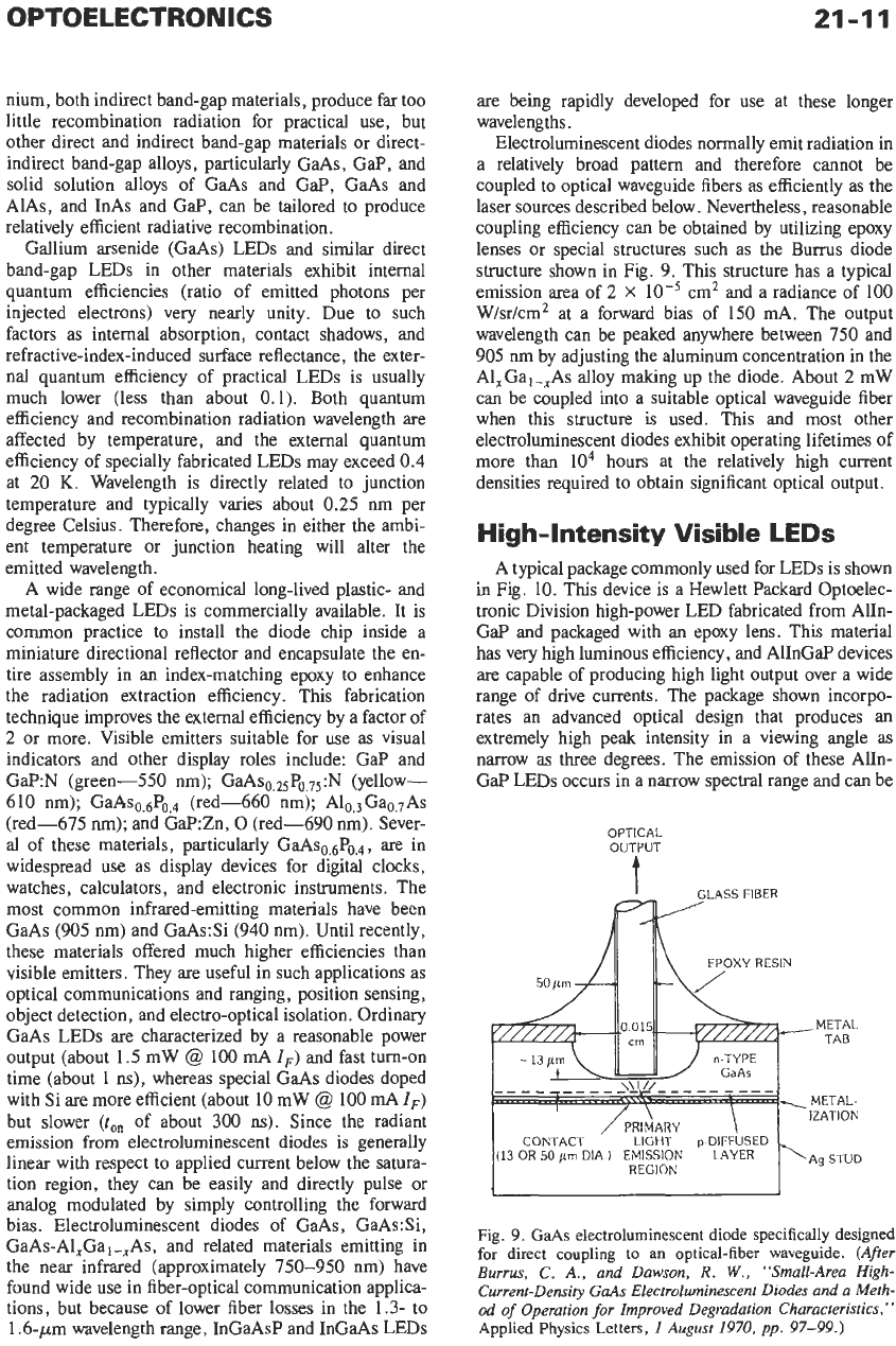
Light-Emitting Diodes§
The operation
of
light-emitting diodes (LEDs) is
dependent on the radiative recombination of electron-
hole pairs at a forward-biased pn junction. The recom-
bination of holes and electrons that occurs when current
is injected into a pn junction results in the release
of
energy. This energy, which corresponds to the band
gap, may be in the
form
of a photon (radiative recom-
bination), a series of photons (lattice vibrations, non-
radiative), or both. In some cases, the energy may be
transferred to another electron. Light-emitting diodes
are electroluminescent diodes in which radiative recom-
bination is significant. Recombination radiation emitted
by LEDs is peaked at or near the band-gap energy, and
in practical devices ranges from
0.55
pm to 34 pm.
The spectral emission width of a representative device
may be
25-30
nm, and this provides sufficient mono-
chromaticity for the production of discrete wavelength
bands (including the visible colors green, yellow,
orange, and red).
Direct band-gap semiconductors make more efficient
LEDs
than indirect band-gap semiconductors (those in
which electron-hole recombination is accompanied by
emission of a photon and phonons). Silicon and germa-
I
Saleh,
B.
E.
A,,
and Teich,
M.
C.
Fundamentals
of
Photonics.
New
York:
John Wiley and Sons (Wiley Inter-
science), 199 1.
OPTOELECTRONICS
21-11
nium, both indirect band-gap materials, produce far too
little recombination radiation for practical use, but
other direct and indirect band-gap materials
or
direct-
indirect band-gap alloys, particularly GaAs, GaP, and
solid solution alloys of GaAs and GaP, GaAs and
AlAs, and InAs and GaP, can be tailored to produce
relatively efficient radiative recombination.
Gallium arsenide (GaAs) LEDs and similar direct
band-gap LEDs in other materials exhibit internal
quantum efficiencies (ratio of emitted photons per
injected electrons) very nearly unity. Due to such
factors as internal absorption, contact shadows, and
refractive-index-induced surface reflectance, the exter-
nal quantum efficiency of practical LEDs is usually
much lower (less than about
0.1).
Both quantum
efficiency and recombination radiation wavelength are
affected by temperature, and the external quantum
efficiency of specially fabricated LEDs may exceed
0.4
at
20
K.
Wavelength is directly related to junction
temperature and typically varies about
0.25
nm per
degree Celsius. Therefore, changes in either the ambi-
ent temperature or junction heating will alter the
emitted wavelength.
A
wide range of economical long-lived plastic- and
metal-packaged LEDs is commercially available. It
is
common practice to install the diode chip inside a
miniature directional reflector and encapsulate the en-
tire assembly in
an
index-matching epoxy to enhance
the radiation extraction efficiency. This fabrication
technique improves the external efficiency by a factor of
2
or more. Visible emitters suitable for use as visual
indicators and other display roles include: GaP and
GaP:N (green-550 nm); G~AS~,~~P,,~~:N (yellow-
610 nm); GaAso.bP0,, (red-660 nm); Alo,3Gao,7As
(red-675 nm); and GaP:Zn,
0
(red-690 nm). Sever-
al of these materials, particularly G~AS~,~P~,~, are in
widespread use as display devices for digital clocks,
watches, calculators, and electronic instruments. The
most common infrared-emitting materials have been
GaAs (905 nm) and GaAs:Si (940 nm). Until recently,
these materials offered much higher efficiencies than
visible emitters. They are useful in such applications as
optical communications and ranging, position sensing,
object detection, and electro-optical isolation. Ordinary
GaAs LEDs
are
characterized by a reasonable power
output (about
1.5
mW
@
100 mA
IF)
and fast turn-on
time (about 1 ns), whereas special GaAs diodes doped
with Si are more efficient (about
10
mW
@
100
mA
IF)
but slower
(ton
of
about
300
ns). Since the radiant
emission from electroluminescent diodes is generally
linear with respect to applied current below the satura-
tion region, they can be easily and directly pulse or
analog modulated by simply controlling the forward
bias. Electroluminescent diodes of GaAs, GaAs:Si,
GaAs-Al,Ga,-,As, and related materials emitting in
the near infrared (approximately 750-950 nm) have
found wide use in fiber-optical communication applica-
tions, but because of lower fiber losses in the
1.3-
to
1.6-pm wavelength range, InGaAsP and InGaAs LEDs
are being rapidly developed for use at these longer
wavelengths.
Electroluminescent diodes normally emit radiation in
a relatively broad pattern and therefore cannot be
coupled to optical waveguide fibers as efficiently as the
laser sources described below. Nevertheless, reasonable
coupling efficiency can be obtained by utilizing epoxy
lenses or special structures such as the
Burrus
diode
structure shown in Fig. 9. This structure has a typical
emission area of
2
X
cm2 and a radiance
of
100
W/sr/cm2 at a forward bias of
150
mA.
The output
wavelength can be peaked anywhere between
750
and
905 nm by adjusting the aluminum concentration in the
Al,GaI-,As alloy making up the diode. About
2
mW
can be coupled into a suitable optical waveguide fiber
when this structure is used. This and most other
electroluminescent diodes exhibit operating lifetimes of
more than
lo4
hours at the relatively high current
densities required to obtain significant optical output.
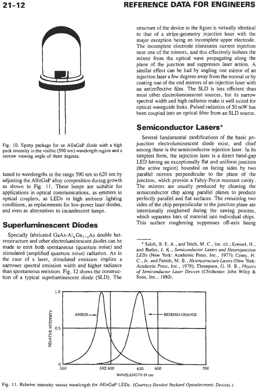
High-Intensity Visible
LEDs
A typical package commonly used for LEDs is shown
in Fig.
10.
This device is a Hewlett Packard Optoelec-
tronic Division high-power LED fabricated from AIIn-
GaP and packaged with an epoxy lens. This material
has very high luminous efficiency, and AlInGaP devices
are capable of producing high light output over a wide
range
of
drive currents. The package shown incorpo-
rates an advanced optical design that produces an
extremely high peak intensity in a viewing angle
as
narrow as three degrees. The emission
of
these AlIn-
GaP LEDs occurs in a narrow spectral range and can be
0
P
T
I
C
A
L
Our
METAL
TAB
LAYER
!lAg
STUD
1113
OR
50
Wtm
DIA
1
EMISSION
’
REGION
Fig.
9.
GaAs electroluminescent diode specifically designed
for direct coupling to an optical-fiber waveguide.
(After
Burrus, C.
A.,
and Dawson,
R.
W.,
“Small-Area High-
Current-Density
GaAs
Electroluminescent Diodes and a Meth-
od
of
Operation for Improved Degradation Characteristics,”
Applied Physics Letters,
I
August
1970,
pp.
97-99.)
21-12
REFERENCE
DATA
FOR
ENGINEERS
n
Fig. 10. Epoxy package for an AlInGaP diode with a high
pack intensity in the visible (590 nm) wavelength region and a
narrow viewing angle of three degrees.
tuned
to
wavelengths in the range
590
nm to
620
nm by
adjusting the AlInGaP alloy composition during growth
as shown in Fig.
11.
These lamps are suitable for
applications in optical communications, as emitters in
optical couplers, as
LEDs
in high ambient lighting
conditions, as replacements for low-power laser diodes,
and even as alternatives to incandescent lamps.
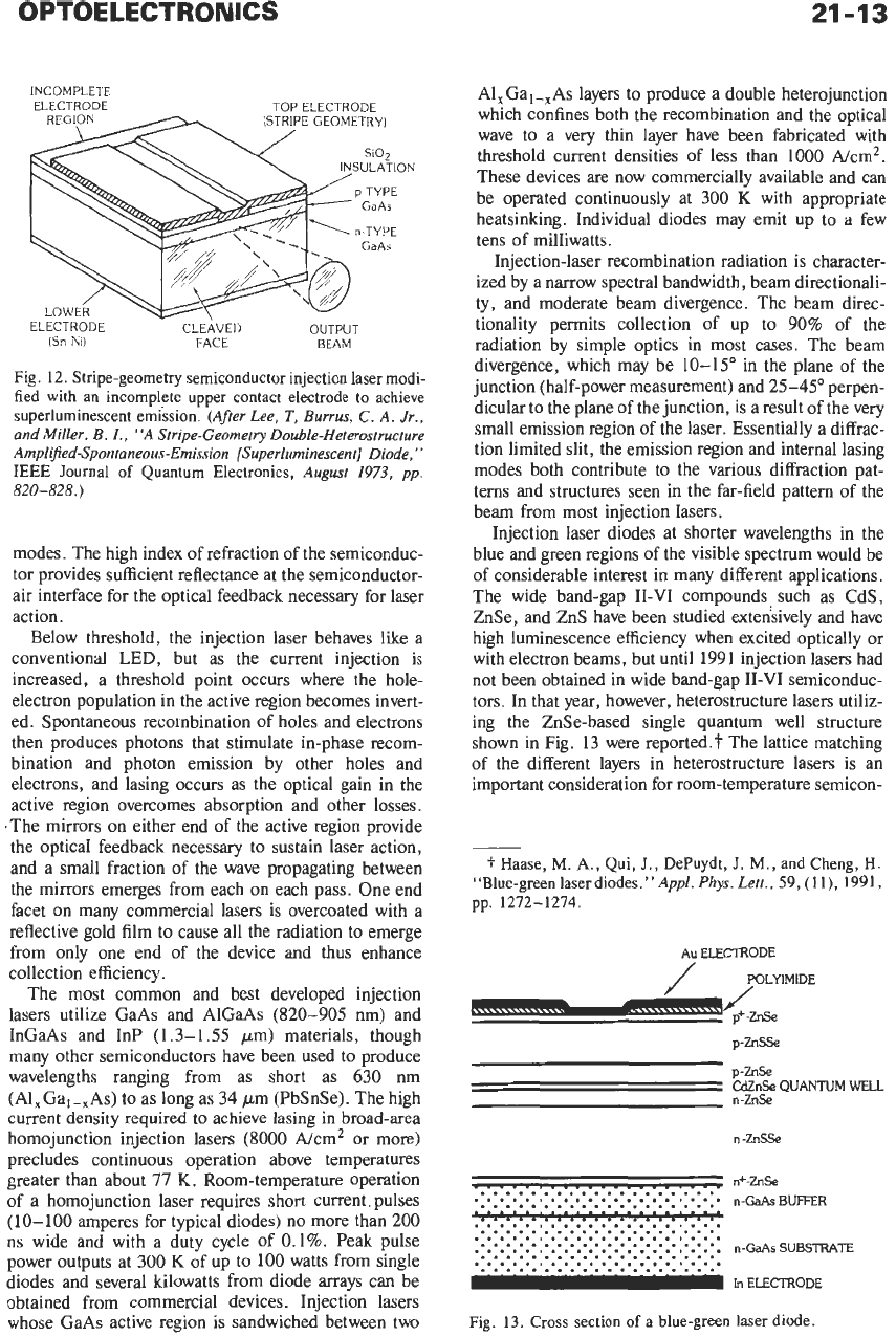
Superluminescent Diodes
Specially fabricated GaAs-Al, Ga
I
-,As double het-
erostructure and other electroluminescent diodes can be
made to emit both spontaneous (quantum noise) and
stimulated (amplified quantum noise) radiation. As in
the case of a laser, stimulated emission implies a
narrower spectral emission width and higher radiance
than spontaneous emission. Fig.
12
shows the construc-
tion of a typical superluminescent diode
(SLD).
The
1.0
k
6
i
o'E
9
2
C
structure of the device in the figure is virtually identical
to that of a stripe-geometry injection laser with the
major exception being
an
incomplete upper electrode.
The incomplete electrode eliminates current injection
near one of the mirrors, and this effectively isolates the
mirror from the optical wave propagating along the
plane of the junction and suppresses laser action. A
similar effect can be had by angling one mirror of an
injection laser a few degrees away from the normal or by
coating one of the end mirrors of an injection laser with
an antireflective film. The
SLD
is less efficient than
most other electroluminescent sources, but its narrow
spectral width and high radiance make it well suited for
optical-waveguide links. Pulsed radiation of
50
mW has
been coupled into an optical fiber from an
SLD
source.
Semiconductor Lasers"
Several fundamental modifications of the basic pn-
junction electroluminescent diode exist, and chief
among these is the semiconductor injection laser. In its
simplest form, the injection laser is a direct band-gap
LED
having an exceptionally
flat
and uniform junction
(the active region) bounded on facing sides by two
parallel mirrors perpendicular to the plane of the
junction, which provide a Fabry-Perot resonant cavity.
The mirrors are usually produced by cleaving the
semiconductor chip along parallel planes to produce
perfectly parallel and flat surfaces. The remaining two
sides of the chip perpendicular to the junction plane are
intentionally roughened during the sawing process,
which separates bars of material into individual chips,
This surface roughening suppresses off-axis lasing
*
Saleh, B. E. A., and Teich,
M.
C., loc. cit.;
Kressel,
H.,
and Butler, J.
K.,
Semiconductor Lasers and Heterojunction
LEDs
(New York: Academic Press, Inc., 1977); Casey,
H.
C.,
Jr. and Panish,
M.
B.,
Heterostructurehsers
(New York:
Academic Press, Inc., 1978); Thompson,
G.
H.
B.,
Physics
of
Semiconductor Laser Devices
(Chichester: John Wiley
&
Sons, Inc., 1980).
--
REDDISH-OWINGE
550
592
600 630 650
700
WAVELENGTH
IN
nrn
Fig.
1
1.
Relative intensity
versus
wavelength for AlInGaP
LEDs.
(Courtesy Hewlett Packard Optoelectronic Devices.)
OPTOELECTRONICS
21-13
INCOMPLETE
ELECTRODE TOP ELECTRODE
STRIPE GEOMETRY)
ELECTRODE CLEAVED OUTPUT
iSn
hi)
FACE BEAM
Fig.
12.
Stripe-geometry semiconductor injection laser modi-
fied
with
an
incomplete upper contact electrode to achieve
superluminescent emission.
(Afer Lee,
T,
Burrus,
C.
A.
Jr.,
and
Miller,
B.
I.,
“A
Stripe-Geometry Double-Heterostructure
Amplijied-Spontaneous-Emission
[Superluminescent]
Diode,”
IEEE
Journal
of
Quantum Electronics,
August
1973,
pp.
820-828.
)
modes. The high index of refraction of the semiconduc-
tor provides sufficient reflectance at the semiconductor-
air interface for the optical feedback necessary for laser
action.
Below threshold, the injection laser behaves like a
conventional
LED,
but as the current injection is
increased, a threshold point occurs where the hole-
electron population in the active region becomes invert-
ed. Spontaneous recombination
of
holes and electrons
then produces photons that stimulate in-phase recom-
bination and photon emission by other holes and
electrons, and lasing occurs as the optical gain in the
active region overcomes absorption and other losses.
’The mirrors on either end of the active region provide
the optical feedback necessary to sustain laser action,
and a small fraction of the wave propagating between
the mirrors emerges from each on each pass. One end
facet on many commercial lasers
is
overcoated with a
reflective gold film to cause all the radiation to emerge
from only one end of the device and thus enhance
collection efficiency.
The most common and best developed injection
lasers utilize GaAs and AlGaAs (820-905 nm) and
InGaAs and InP (1.3-1.55 pm) materials, though
many other semiconductors have been used to produce
wavelengths ranging from as short as 630 nm
(Al,Ga,-,As) to as long as 34
pm
(PbSnSe). The high
current density required to achieve lasing in broad-area
homojunction injection lasers
(8000
A/cm2 or more)
precludes continuous operation above temperatures
greater than about
77
K.
Room-temperature operation
of a homojunction laser requires short current. pulses
(10-100 amperes for typical diodes) no more than 200
ns wide and with a duty cycle of
0.1%.
Peak pulse
power outputs at
300
K
of
up to
100
watts from single
diodes and several kilowatts from diode arrays can be
obtained from commercial devices. Injection lasers
whose GaAs active region is sandwiched between two
AlXGa1-,As layers to produce a double heterojunction
which confines both the recombination and the optical
wave to a very thin layer have been fabricated with
threshold current densities of less than 1000 A/cm2.
These devices are now commercially available and can
be operated continuously at
300
K
with appropriate
heatsinking. Individual diodes may emit up to a few
tens of milliwatts.
Injection-laser recombination radiation is character-
ized by a narrow spectral bandwidth, beam directionali-
ty, and moderate beam divergence. The beam direc-
tionality permits collection of up
to
90% of the
radiation by simple optics in most cases. The beam
divergence, which may be 10-15’ in the plane of the
junction (half-power measurement) and 25-45’ perpen-
dicular
to
the plane of the junction, is a result of the very
small emission region of the laser. Essentially a difiac-
tion limited slit, the emission region and internal lasing
modes both contribute
to
the various diffraction pat-
terns and structures seen in the far-field pattern of the
beam from most injection lasers.
Injection laser diodes at shorter wavelengths in the
blue and green regions of the visible spectrum would be
of considerable interest in many different applications.
The wide band-gap 11-VI compounds, such as CdS
,
ZnSe, and ZnS have been studied extensively and have
high luminescence efficiency when excited optically or
with electron beams, but until 1991 injection lasers had
not been obtained in wide band-gap 11-VI semiconduc-
tors. In that year, however, heterostructure lasers utiliz-
ing the ZnSe-based single quantum well structure
shown in Fig. 13 were reported.? The lattice matching
of the different layers in heterostructure lasers is an
important consideration for room-temperature semicon-
’!
Haase,
M.
A.,
Qui,
J.,
DePuydt,
J.
M.,
and Cheng,
H.
“Blue-green laser diodes.”AppZ.
Phys.
Lett.,
59, (ll), 1991,
pp.
1272-1274.
7
EEm~~iiD~
-1
p+-ZnSe
p-ZnsSe
p-ZnSe
CdZnSe
QUANTUM
WEU
n-ZnSe
n
-ZnsSe
...................
-
...................
....................
...................
2.*.*
am............,
....................
...................
....................
...................
....................
...................
....................
n+-ZnSe
n-GaAs
BUFFER
n-GaAs
SUBSTRATE
In ELECTRODE
Fig.
13.
Cross
section
of a
blue-green laser diode.
21-14
REFERENCE DATA FOR ENGINEERS
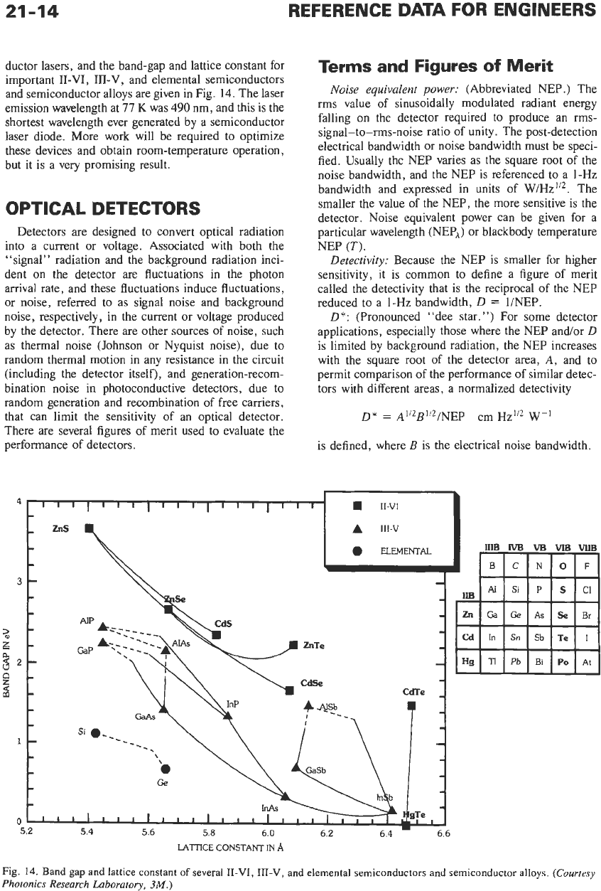
ductor lasers, and the band-gap and lattice constant for
important
11-VI, 111-V,
and elemental semiconductors
and semiconductor alloys are given in Fig.
14.
The laser
emission wavelength at
77
K
was
490
nm, and this is the
shortest wavelength ever generated by a semiconductor
laser diode. More work will be required to optimize
these devices and obtain room-temperature operation,
but it is a very promising result.
OPTICAL DETECTORS
Detectors are designed to convert optical radiation
into a current or voltage. Associated with both the
“signal” radiation and the background radiation inci-
dent on the detector are fluctuations in the photon
arrival rate, and these fluctuations induce fluctuations,
or noise, referred to as signal noise and background
noise, respectively, in the current or voltage produced
by the detector. There are other sources of noise, such
as thermal noise (Johnson or Nyquist noise), due to
random thermal motion in any resistance in the circuit
(including the detector itself), and generation-recom-
bination noise in photoconductive detectors, due to
random generation and recombination
of
free carriers,
that can limit the sensitivity of an optical detector.
There are several figures of merit used to evaluate the
performance of detectors.
Terms
and
Figures
of
Merit
Noise equivalent power:
(Abbreviated NEP
.)
The
rms value of sinusoidally modulated radiant energy
falling on the detector required to produce an rms-
signal-to-rms-noise ratio of unity. The post-detection
electrical bandwidth or noise bandwidth must be speci-
fied. Usually the NEP varies as the square root of the
noise bandwidth, and the NEP is referenced to a 1-Hz
bandwidth and expressed in units of W/Hz”*. The
smaller the value
of
the NEP, the more sensitive is the
detector. Noise equivalent power can be given for a
particular wavelength (NEPJ or blackbody temperature
NEP
(T).
Detectivity:
Because the NEP is smaller for higher
sensitivity, it is common to define a figure of merit
called the detectivity that is the reciprocal of the NEP
reduced to a 1-Hz bandwidth,
D
=
1/NEP.
D*:
(Pronounced “dee star.”) For some detector
applications, especially those where the NEP and/or
D
is limited by background radiation, the NEP increases
with the square root of the detector area, A, and to
permit comparison of the performance of similar detec-
tors with different areas, a normalized detectivity
D*
=
A’/ZBI’Z/NEP cm HZ”~
W-I
is defined, where
B
is the electrical noise bandwidth
Fig.
14.
Band gap and lattice constant
of
several
11-VI, 111-V,
and elemental semiconductors and semiconductor alloys.
(Courtesy
Photonics Research Laboratory,
3M.)
21-15
Because of the way infrared detectors
are
character-
ized, it is common to specify the D* as D*bb or D*, to
indicate measurement of the D* with a blackbody or
with a monochromatic source. Usually,
D*
is given as
(T,
f,
Af)
for a blackbody temperature
T,
chop-
ping frequency
f,
and bandwidth
Af,
and D*A
(A,
f,
Af)
for measurement or evaluation at wavelength
A,
chop-
ping frequency
f,
and bandwidth
Af.
tivity of a background-limited detector depends not
only on the temperature of the background but, for
cooled detectors, also on the field of view.
As
the field
of view is decreased, the background radiation is
reduced, and the detectivity is increased,
so
long as the
detectivity is limited by the background radiation. The
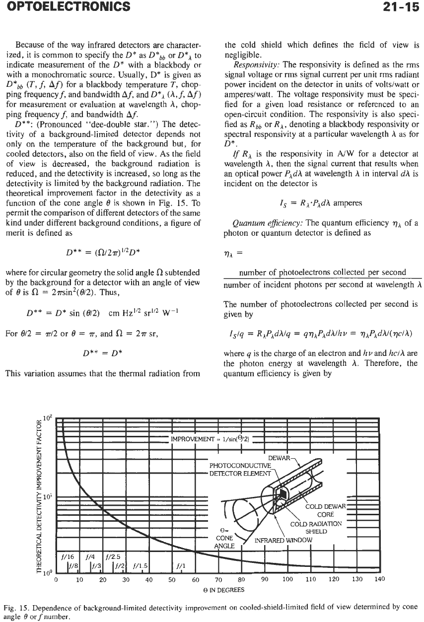
theoretical improvement factor in the detectivity as a
function of the cone angle
t9
is shown in Fig.
15.
To
permit the comparison of different detectors of the same
kind under different background conditions, a figure of
merit is defined as
D**.
.
(Pronounced “dee-double star.”) The detec-
D**
=
(fl2/2.rr)”*D*
where for circular geometry the solid angle
fl
subtended
by the background for a detector with
an
angle of view
of
t9
is
fl
=
2min2(8/2). Thus,
D** =D* sin
‘
(812) cm
HZ”~
sr1’2
W-’
For 812
=
1~12 or
8
=
IT, and
R
=
2a sr?
D**
=
D”
This variation assumes that the thermal radiation from
the cold shield which defines the field of view
is
negligible.
Responsivity:
The responsivity is defined as the
rms
signal voltage or
rms
signal current per unit rms radiant
power incident on the detector in units of voltslwatt or
ampereslwatt. The voltage responsivity must be speci-
fied for a given load resistance or referenced to an
open-circuit condition. The responsivity is also speci-
fied as
Rbb
or
RA
,
denoting a blackbody responsivity or
spectral responsivity at a particular wavelength
A
as for
D*.
If
RA
is the responsivity in
A/W
for a detector at
wavelength
A,
then the signal current that results when
an optical power
PAdh
at wavelength
A
in interval
dA
is
incident on the detector is
I,
=
RAaPAdh
amperes
Quantum
eflciency:
The quantum efficiency
qA
of a
photon or quantum detector is defined as
qA
=
number of photoelectrons collected per second
number of incident photons per second at wavelength
A
The number of photoelectrons collected per second is
given by
Is19
=
RAPAdAlq
=
qqAPAdAlhv
=
~~P~dA/(~CIA)
where
q
is the charge of an electron and hvand
hclA
are
the photon energy at wavelength
A.
Therefore, the
quantum efficiency is given by
e
IN
DEGREES
Fig.
15.
Dependence
of
background-limited detectivity improvement
on
cooled-shield-limited field
of
view determined by cone
angle
0
orfnumher.