Middleton W.M. (ed.) Reference Data for Engineers: Radio, Electronics, Computer and Communications
Подождите немного. Документ загружается.

20-1
10
processing,”
IEEE Trans. on Electron Devices,
Vol. 39, No. 1, 1992, p. 4.
50. Moslehi, M., Kuehne, J., Velo, L., Yin, D., Yeak-
ley, D., Huang,
S.,
Jucha, B., and Breedijk, T.
“RTP for advanced CMOS process integration.”
Proc. of SPIE
on
Rapid Thermal and Integrated
Processing,
1992.
51. Moslehi, M., Kuehne,
J.,
Yealdey, R., Velo, L.,
Najm, H., Dostalik, B., Yin, D., and Davis, C.
“In-situ fabrication and process control tech-
niques in rapid thermal processing.”
MRS Proc.
on Rapid Thermal and Integrated Processing,
Vol. 224, 1991, p. 143.
52. Moslehi, M. M. “Process uniformity and slip dis-
location patterns
in
linearly ramped-temperature
transient rapid thermal processing of silicon.”
IEEE Trans.
on
Semiconductor Manufacturing,
Vol. 2, No. 4, 1989, p. 130.
53. Gyurcsik, R.
S.,
Riley, T. J., and Sorrell, F. Y.
IEEE Trans.
on
Semiconductor Manufacturing,
Vol. 4, No. 1, 1991, p. 9.
54. Campbell,
S.,
Knutson, K., Ahn, K., Leighton, J.,
and Liu, B. “Gas flow patterns and thermal uni-
formity in rapid thermal processing equipment.”
IEDM Tech. Dig.,
1990, p. 921.
55.Sorre1, F.
SRC workshop
on
temperature mea-
surement,
Santa Fe, New Mexico, Feb. 1990.
56. Nulman,
J.,
Cohen, B., Blonigan, W., Antonio,
S.,
Meinecke, R., and Gat, A. “Pyrometric emissivity
measurements and compensation in an RTP
chamber.”
MRS Symp. Proc.,
Vol. 146, 1989, p.
461.
57. Sato, T.
Jpn.
J.
Appl.
Phys.,
Vol. 6, 1967, p. 339.
58. Gelpey,
J.,
and Liao,
J.
“Integrated temperature
control with automatic emissivity compensation
for RTP.”
SRC workshop on temperature mea-
surement,
Santa Fe, New Mexico, Feb. 1990.
59. Kamins, T., Bradbury, D., Cass, T., Laderman, S.,
and Reid, G. “Structure of LPCVD tungsten films
for IC applications.”
J.
Electrochem. SOC.,
Vol.
131, Dec. 1986, p. 2555.
60. Kern, W. “The evolution of silicon cleaning tech-
nology.”
Proc.
of
the First International Symp.
on
Cleaning Technol. in Semiconductor Device Mfg.
(The Electrochem. SOC.),
Vol. 90-9, 1989,
p.
3.
61. Deal,
B.,
and Kao,
D.
“The physics and chemistry
of
thin native oxide
films
on silicon,”
Mat. Res.
SOC. Symp.,
1987.
62. Moslehi, M., Shatas, S., Saraswat, K., and Meindl,
J. “Interfacial and breakdown characteristics of
MOS devices with rapidly grown ultra-thin Si02
gate insulators.”
IEEE Trans. Electron Devices,
63. Morita, M., Ohmi, T., Hasegawa, E., Kawakami,
M., and Suma, K. “Control factor
of
native oxide
growth
on
silicon in air
or
in ultra-pure water.”
Appl.
Phys. Lett.,
Vol. 55, No. 6, 1989, pp. 562-
564.
64. Hirashita, N., Kinoshita, M., Aikawa,
I.,
and
Ajioka, T. “Effects of surface hydrogen
on
the
air
Vol.
ED-34,
NO. 6, 1987, pp. 1407-1410.
oxidation at room temperature of HF-treated
Si(100) surfaces.”
Appl.
Phys. Lett.,
Vol. 56,
No.
5, 1990, pp. 451453.
65. Crabbe, E., Hoyt,
J.,
Moslehi, M., Pease, R., and
Gibbons, J. “Reduced process sensitivity
of
poly-
silicon emitter contacts for VLSI bipolar transis-
tors.”
Symp. on VLSI Technol. Dig. Tech. Papers,
66. Burrows, V., Chabal, Y., Higashi, G., Raghavva-
chari, K., and Christman,
S.
“Infrared spectros-
copy of
Si(ll1)
surfaces after HF treatment:
Hydrogen termination and surface morphology.”
Appl.
Phys. Lett.,
Vol. 53, No. 11, 1988, pp. 998-
1000.
67. Miyauchi, A., Inoue, Y., and Suzuki,
T.
“Interface
impurities
of
low-temperature (900
“C)
deposited
Si epitaxial films prepared by HF treatments.”
Appl.
Phys. Lett.,
Vol. 57, No. 7, 1990, p. 676.
68. Friedrich,
J.,
and Neudeck, G. “Limitations
in
low-temperature silicon epitaxy due
to
water
vapor and oxygen in the growth ambient.”
Appl.
Phys. Lett.,
Vol. 53,
No.
25, 1988, pp. 2543-2545.
69. Ruzyllo,
J.,
Hoff,
A., Frystak,
D.,
and Hossain,
S.
“Electrical evaluation
of
wet and
dry
cleaning
procedures for silicon device fabrication.”
J.
Electrochem. SOC.,
Vol. 136, No. 5, 1989, pp.
1474-1476.
70. Mieno, F., Nakamura,
S.,
Deguchi,
T.,
Maeda,
M., and Inayoshi, K. “Low temperature silicon
epitaxy using Si,H,.”
J.
Electrochem. SOC.,
Vol.
134,
No.
9,1987, pp. 2320-2323.
7
1.
Yamazaki, T., Minakata, H., and Ito, T. “Continu-
ous
growth
of
heavily doped p+-ncSi epitaxial
layer using low-temperature photoepitaxy.”
Appl.
Phys. Lett.,
Vol.
55,
No.
9, 1989, pp. 879-881.
72. Yamazaki, T., Watanabe, S., and Ito, T. “Heavy
boron doping in low-temperature Si photoepit-
axy,”
J.
Electrochem. SOC.,
Vol. 137, No. 1, 1990,
73. Meyerson, B., LeGoues,
E,
Nguyen, T., and
Harame, D. “Nonequilibrium boron doping
effects in low-temperature epitaxial silicon films.”
Appl.
Phys. Lett.,
Vol.
50,
No.
2, 1987, pp. 113-
115.
74. Meyerson,
B.,
Uram, K., and LeGoues,
E
“Coop-
erative growth phenomena in silicon/germanium
low-temperature epitaxy.”
Appl.
Phys. Lett.,
Vol.
75. Shibata, T., Kondo,
N.,
and Nanishi, Y. “Si sur-
face cleaning and epitaxial growth of GaAs on
Si
by electron cyclotron resonance plasma-excited
molecular-beam-epitaxy at low temperatures.”
J.
Electrochem. SOC.,
Vol. 136, No. 11, 1989, pp.
76. Salimian,
S.,
Cooper, C., and Ellingboe, A. “Etch-
ing of SiO, in an electron cyclotron resonance
argon plasma.”
Appl.
Phys. Lett.,
Vol. 56, No. 14,
77. Moslehi M., and Davis, C. “Advanced epitaxial Si
and Ge,Si,, multiprocessing for semiconductor
1987, pp. 33-34.
pp. 313-318.
53,
NO.
25,1988, pp. 2555-2557.
3459-3462.
1990, pp. 1311-1313.
20-1
I1
device technologies.”
J.
Mat. Res.,
Vol. 5, No. 6,
78. Miki, N., Kikuyama, H., Kawanabe,
I.,
Miya-
shita, M., and Ohmi,
T.
“Gas-phase selective
etching of native oxide.”
IEEE Trans. Electron
Devices,Vol.
37,
No.
1, 1990, pp. 107-115.
79. Syverson, D., and Duranko, G. “Contamination
aspects of anhydrous HF gas processing.”
Solid
State Technol.,
1988, pp. 101-104.
80.
Deal, B., McNeilly,
M.,
Kao, D., and de Larios, J.
“Vapor phase wafer cleaning thin film, oxide
etching, and thin film growth.”
Proc. of the First
International Symp. on Cleaning Technol. in
Semiconductor Device Mfg. (The Electrochem.
81.
Sedgwick,
T.,
Berkenblit, M., and Kuan,
T.
“Low-
temperature selective epitaxial growth of silicon
at atmospheric pressure.”
Appl. Phys. Lett.,
Vol.
54, No. 26,1989, pp. 2689-2691.
82. Campbell,
S.,
Leighton,
J.,
Case,
G.,
and Knut-
son, K. “Very
thin
silicon epitaxial layers grown
using rapid thermal vapor phase epitaxy.”
J.
Vac.
Sci. Technol.,
Vol.
B7,
No.
5, 1989, pp. 1080-
1083.
83. Regolini,
J.,
and Bensahel, D. “Selective epitaxial
silicon growth in the
650-1100
“C range in a
reduced pressure chemical vapor deposition reac-
tor using dichlorosilane.”
Appl. Phys. Lett.,
Vol.
84. Gibbons,
J.,
King, C., Hoyt,
J.,
Noble, D., Gronet,
C., Scott, M., Rosner,
S.,
Reid,
G.,
Laderman,
S.,
Nauka, K., Turner, J., and Kamins,
T.
“Si/Si,_,Ge,
heterojunction bipolar transistors fabricated by
limited reaction processing.”
IEDM Tech. Dig.,
1988, pp. 566-569.
85. Yew, T., and Reif, R. “Silicon selective epitaxial
growth at
800
“C using SiHflz assisted by HJAr
plasma sputter.”
Appl. Phys. Lett.,
Vol.
55,
No.
10,
1989, pp. 1014-1016.
86. Ohmi,
T.,
Hashimoto, K., Morita, M., and Shi-
bata,
T.
“In situ-doped epitaxial silicon film
grown at 250 “C by
an
ultra-clean low-energy
bias sputtering.”
IEDM Tech. Dig.,
1989, pp. 53-
56.
87. Ohmi, T. “Future trends and applications of ultra-
clean technology.”
IEDM Tech. Dig.,
1989, pp.
88.
Gao,
Q., Hariu, T., and
Ono,
S.
“Low-temperature
surface cleaning
of Si
and successive plasma-
assisted epitaxial growth of GaAs.”
Jpn.
J.
Appl.
Phys.,
Vol. 26,
No.
10, 1987, pp. L1576-Ll578.
89. Sherman, A.
“In
situ removal of native oxide
from silicon wafers.”
J.
Vnc. Sci. Technol.
B,
Vol.
90. Miyake,
K.
“Removal of
a
thin SiO, layer by low-
energy hydrogen ion bombardment at elevated
temperatures.”
Jpn.
J.
Appl. Phys.,
Vol. 28, No.
91. Yamada,
H.
“Low-temperature surface cleaning
method using low-energy reactive ionized spe-
1990, pp. 1159-1162.
SOC.),
Vol. 90-9, 1989, p. 121.
54,
NO.
7, 1989, pp. 658-659.
49-52.
8,
NO. 4, 1990, pp. 656-657.
11,1989, pp. 2376-2381.
cies.”
J.
Appl. Phys.,
Vol. 65, No. 2, 1989, pp.
775-78 1.
92. Suemune,
I.,
Kishimoto, A,, Hamaoka, K.,
Honda,
Y.,
Kan, Y., and Yamanishi, M. “Depen-
dence of GaAs etch rate on the angle of incidence
of
a
hydrogen plasma beam excited by electron
cyclotron resonance.”
Appl. Phys. Lett.,
Vol. 56,
No. 24,1990, pp. 2393-2395.
93.Breaux, L., Anthony, B., Hsu,
T.,
Banerjee, S.,
and Tasch, A. “Homoepitaxial films grown in
Si(100)
at
150 “C by remote plasma-enhanced
chemical vapor deposition.”
Appl. Phys. Lett.,
94. Burns, G. “Low-temperature native oxide
removal from silicon using nitrogen trifluoride
prior to low-temperature silicon epitaxy.”
Appl.
Phys. Lett.,
Vol. 53,
No.
15, 1988, pp. 1423-1425.
95. Saito, Y., Yamaoka,
O.,
and Yoshida, A. “Plasma-
less cleaning process of silicon surface using
chlorine trifluoride.”
Appl. Phys. Lett.,
Vol. 56,
96.Hirose,
E,
Suemitsu, M., and Miyamoto, N.
“High quality silicon epitaxy at
500
“C using
silane gas-source molecular beam technique.”
Jpn.
J.
Appl. Phys.,
Vol. 28, No. 11, 1989, pp.
97. Murota,
J.,
Nakamura, N., Kato, M., and Miko-
shiba, N. “Low-temperature silicon selective depo-
sition and epitaxy on silicon using the thermal
decomposition of silane under ultraclean environ-
ment.”
Appl. Phys. Lett.,
Vol.
54,
No.
11, 1989,
98. Morar,
J.,
Meyerson,
B.,
Karisson,
U.,
Himpsel,
F., and McFeely,
E
“Oxygen removal from Si via
reaction with absorbed Ge.”
Appl. Phys. Lett.,
Vol.
50,
No.
8,
1987, pp. 463-465.
99. Novak, R. “Anhydrous HF etching of native
SiO,:
Applications
to
device fabrication.”
Solid State
Technol.,
March 1988, pp. 3941.
100. Deal, B., McNeilly, M., Kao, D., and delarios,
J.
“Vapor phase wafer cleaning: Processing for the
1990s.”
Solid State Technol.,
July 1990, pp. 73-
77.
101. Miki, N., Kikuyama,
H.,
Maeno, M., Murota,
J.,
and Ohmi, T. “Selective etching of native oxide
by
dry
processing using ultra clean anhydrous
hydrogen fluoride.”
IEDM
Tech. Dig.,
1988. pp.
102. Nara, Y., Yamazaki,
T.,
Sugii,
T.,
Sugino,
R.,
Ito,
T., and Ishikawa,
H.
“Photochemical cleaning and
epitaxy of
Si.”
SPIE
Symp.
on
Advances in Semi-
conductors and Semiconductor Structures,
Pan-
ama City, 1988.
103. Takahagi,
T.,
Nagai,
I.,
Ishitani, A., and Kuroda,
H. “The formation
of
hydrogen passivated silicon
single-crystal surfaces using ultraviolet cleaning
and HF etching.”
J.
Appl. Phys.,
Vol. 64, No. 7,
1988, pp. 3516-3521.
104. Vig,
J.
“W/ozone cleaning
of
surfaces.”
Proc. of
the First International Symp. on Cleaning Technol.
Vol.
55,
NO.
18,
1989, pp. 1885-1887.
NO. 12, 1990,~~. 1119-1121.
L2003-L2006.
pp. 1007-1009.
730-733.
20-1
12
in
Semiconductor Device
Mfg.
(The Electrochem.
105.
Itoh,
T.,
Sugino, R., Watanabe, S., Nara,
Y.,
and
Sato,
Y.
“UV enhanced
dry
cleaning of silicon
wafers.”
Proc.
of
the First International Symp.
on
Cleaning Technol. in Semiconductor Device
Mfg.
(The Electrochem.
Soc.),
Vol. 90-9, 1989, p. 114.
106. Logan,
J.
S.,
Costable,
J.,
and Jones, F., “High
rate radio frequency sputtering using in-phase
plasma confinement.”
J.
Vac.
Sei.
Technol.
A,
Vol.
8, 1990, p. 1835.
107. Honvitz, C. M. “Silicon deposition in diode and
hollow cathode systems.”
J.
Vue.
Sei.
Technol.
B,
Vol. 7, 1989, p. 443.
108.Horwitz, C. M., Boronkay, S., Gross,
M.,
and
Davies, K. “Hollow cathode etching and deposi-
tion.”
J.
VUC.
Sei.
Technol. A,
Vol. 6, 1988, p. 1837.
109. Davies, K. E., and Honvitz, C. M. “Diode and
hollow cathode etching in CF,,”
J.
Vue.
Sei.
Tech-
7201.
A,
Vol. 7, 1989, p. 270.5.
110. Shirakawa, T., Toyoda, H., and Sugai, H. “RF
plasma production
at
ultralow pressures with sur-
face magnetic confinement.”
J.
Vac.
Sei.
Technol.
B.
Vol. 7, 1989, p. 443.
111. Cook,
J.
M., Ibbotson, D. E., and Flamm, D.
L.
“Application of
a
low-pressure radio frequency
discharge source to polysilicon etching.”
J.
VUC.
Sei.
Technol.
B,
Vol. 8, 1990, p. 1.
112. Kitagawa,
A.,
Takeuchi, M., and Kasagi, M.
“Enhanced growth of silicon dioxide films by
parallel resonant RF plasmas.”
Jpn.
J.
Appl.
Phys.,
Vol. 7, 1990, p. L1178.
113. Keller,
J.
H. “Novel RF induction plasma pro-
cessing techniques.”
Abstracts
of
37th Amer. Vac.
Soc.
Symp.,
Toronto, 1990.
114. Boswell, R. W., and Porteous, R.
K.
“Large vol-
ume high density
RF
inductively coupled
plasma.”Appl.
Phys. Lett.,
Vol. 50, 1987, p. 1130.
115. Boswell, R. W., Perry, A.
J.,
and Emami,
M.
“Multipole confined diffusion plasma produced
by 13.56 MHz electrodeless source,”
J.
Vue.
Sei.
Technol.
A,
Vol. 7, 1989, p. 3345.
116. Thornton,
J.
A. “Magnetron sputtering: Basic
physics and applications to cylindrical magne-
trons,”
J.
Vue.
Sei.
Technol.,
Vol.
15,
1978, p. 171.
117.
Yeom,
G.
Y.,
and Kushner,
M.
J.
“Magnetic field
effects on cylindrical reactive ion etching of
Si/SiO, in CFfl, plasmas,”
J.
Vue.
Sei.
Technol.
A,
Vol.
7, 1989, p. 987.
118. Bright,
A. A.,
and Kaushik, S. “Magnetron ion
etching with CF, based plasmas: Effects
of
mag-
netic field on plasma chemistry.”J.
Vac.
Sei.
Tech-
nol.
B,
Vol. 7, 1990, p. 542.
119. Sheridan, T. E., Goeckner, M.
J.,
and Goree,
J.
“Model
of
energetic electror, transport in magne-
tron discharges.”
J.
Vac.
Sei.
Technol.
A,
Vol.
8,
1990, p. 30.
120. Wendt, A.
E.,
and Lieberman, M.
A.
“Spatial
structure of
a
planar magnetron discharge.”
J.
Vue.
Sei.
Technol.
A,
Vol. 8, 1990, p. 902.
SOC.),
Vol. 90-9, 1989, p. 105.
121. Okano, H., Horiike,
Y.,
and Yamazaki, T. “Etch-
ing characteristics of n+ poly-Si and A1 employ-
ing
a
magnetron plasma.”
Jpn.
J.
Appl.
Phys.,
Vol.
23, 1984, p. 482.
122. Asmussen,
J.
“Electron cyclotron resonance
microwave discharges for etching and thin film
deposition.”
J.
VUC.
Sei.
Technol.
A, Vol. 7, 1989,
p.
883.
123.Shufflebotham, P. K., and Thompson, D.
J.
“Diagnostic techniques for plasma stability in
electron cyclotron plasma processing.”
J.
Vac.
Sei.
Technol.
A,
Vol. 8, 1990, p. 3713.
124. Uetake, H., Matsuura, T., and Ohmi, T. “Anisotro-
pic etching
of
n’ polycrystalline silicon with high
selectivity using
a
chlorine and nitrogen plasma
in an ultraclean electron cyclotron resonance
etcher.”Appl.
Phys. Lett.,
Vol. 57, 1990, p. 596.
125. Matsuo,
S.,
and Adachi,
Y.
“Reactive ion etching
using
a
broad beam ECR ion source.”
Jpn.
J.
Appl. Phys.,
Vol. 21, 1982, p. L4.
126. Burke, R. R., Pelletier,
J.,
Pornot, C., and Vallier,
L. “Distributed electron cyclotron resonance in
silicon processing: epitaxy and etching.”
J.
Vac.
Sei.
Technol. A,
Vol.
8,
1990, p. 2931.
127. Constantine, C., Johnson, D., Pearton, S.
J.,
Chakrabarti,
U.
K., Emerson, A. B., Hobson,
W. S., and Kinsella, A.
P.
‘‘Plasma etching of JI-V
semiconductors in CH@I,/Ar electron cyclotron
resonance discharges.”
J.
Vac. Sei. Technol. A,
Vol. 8, 1990, p. 596.
128. Popov,
0.
A., and Waldron, H. “Electron cyclo-
tron resonance plasma stream source for plasma
enhanced chemical vapor deposition.”
J.
Vac.
Sei.
Technol. A,
Vol. 7, 1989, p. 914.
129. Wei,
J.,
Kawarada, H., and Suzuki,
J.
“Low tem-
perature synthesis
of
diamond films using
magneto-microwave plasma CVD.”
Jpn.
J.
Appl.
Phys.,
Vol. 29, 1990, p. L1483.
130. Ono,
T.,
Oda, M., Takahashi, C., and Matsuo, S.
“Reactive ion stream etching utilizing electron
cyclotron resonance plasma.”
J.
Vue.
Sei.
Technol.
B,
Vol. 4, 1988, p. 696.
131. Holber, W. M., and Forster,
J. “Ion
energetics in
electron cyclotron resonance discharges.”
J.
Vue.
Sei.
Technol.
A, Vol. 8, 1990, p. 3720.
132. Samukawa,
S.,
Mori,
S.,
and
Sasaki,
M.
“Depen-
dence of ECR plasma etching characteristics on
sub magnetic field and substrate position.”
Jpn.
J.
Appl. Phys.,
Vol. 29, 1990, p. 792.
133. Hopwood,
J.,
Reinhard, D.
K.,
and Asmussen,
J.
“Charged particle densities and energy distribu-
tions in
a
multipolar electron cyclotron resonance
plasma etching source.”
J.
Vue.
Sei.
Technol.
A,
Vol. 8, 1990, p. 3103.
134. Pichot, M., and Durandet, A. “Microwave multi-
polar plasmas excited by distributed electron
cyclotron resonance: Concept and performance.”
Rev.
Sei.
Instrum.,
Vol. 59, 1988, p. 1072.
135. Tachi, S., Tsujimoto, K., and Okudaira, S. “Low-
temperature reactive ion etching and microwave
plasma etching
of
silicon.”
Appl. Phys. Lett.,
Vol.
52,
No.
8,
1988, p. 616.
136. Izumi, K., et al.
Trans. Inst. Elect. and Comm.
Eng. Jpn. Sect. E
(Japan), Vol. E62, No. 12, Dec.
1979,
p.
921.
137. Bumham,
M.
E., and Wilson,
S.
R.
Proc. SPIE,
Vol. 530, 1985, p. 240.
138. Hemment, P.
L.
E
Mater. Res. SOC. Symp. Proc.,
Vol. 53, 1986, p. 207.
139. Mao, B.-Y., et al,
IEEE Trans. Nucl. Sci.
Vol.
NS-
33,
No.
6, 1986, p. 1702.
140. Davis,
G.
E., et al.
IEEE Trans. Nucl. Sci.,
Vol.
141. Colinge, J. P.
Silicon On Insulator Technology:
Materials to VLSI.
Dordrecht: Kluwer Academic
Publishers, 1991.
142. Bailey, W.
E.,
Lu,
H., Blake,
T.
G.
W.,
Hite, L.
R.,
Mei,
P.,
Hurta, D., Houston,
T.
W.,
and Pollack,
G.
P.
1991
IEEE International
SOI
Conference
Proceedings,
199 1, p. 134.
143. McKitterick,
J.
B., and Caviglia, A.
L.
IEEE
Trans. Elect. Dev.,
Vol. 36,
No.
6, 1989,
p.
1133.
NS-32, NO. 6, 1985,
p.
4432.
144. Celler,
G.
K.,
et al.
1989
IEEE
SOSISOI
Technol-
ogy Conference Proceedings,
1989, p. 139.
145. Mayer,
D.
I989
IEEE
SOSISOI
Technology Con-
ference Proceedings,
1989, p. 52. Hashimoto,
K.,
et al.
IEDM Technical Digest,
1985, p. 672.
146. Houston,
T.
W.,
Lu,
H.,
Mei, P., Blake,
T.
G.
W.,
Hite, L.
R.,
Sundaresan,
R.,
Matloubian, M.,
Bailey,
W.
E., Liu, J., Peterson, A., and Pollack,
G.
IEEE
SOSISOI
Technology Conference Pro-
ceedings,
1989, Paper L1, p. 137.
147.
Miki,
H., Omura,
Y.,
Ohmameuda,
T.,
Kumon,
M.,
Asada,
K.,
Izumi,
K.,
Sakai,
T.,
and Sugano,
T.
IEDM Tech. Dig.,
1989, Paper 34.7.1, p. 906.
148. Yamazaki, K., et
al.
Ext. Abstracts ofthe 8th Inter-
nat. Workshop on Future Electron Devices-Three
Dimensional
ICs
and Nano-Meter Functional
Devices, Kochi Prefecture, Japan,
1990, p. 105.
149. Aibara,
R.,
et al.
Ext. Abstracts
of
the 8th Inter-
nat. Workshop on Future Electron Devices-
Three Dimensional ICs and Nano-Meter Func-
tional Devices, Kochi Prefecture, Japan,
1990,
p. 113.
21
Optoelectronics
Revised
and
Expanded
by
Gregory
E.
Stillman
The Optical Spectrum
21-2
Radiometry
21-3
Terms and Definitions
Blackbody Radiation
Interaction
of
Optical Waves With Matter
21-9
Reflectance
Absorptance
Transmittance
Refraction
Optical Sources
21-10
Tungsten Lamps
Fluorescent Lamps
Arc Lamps
Light-Emitting Diodes
High-Intensity Visible LEDs
Superluminescent Diodes
Semiconductor Lasers
Optical Detectors
21-14
Terms
and
Figures
of
Merit
Characterization
of
Detectors
Ultimate Sensitivity
of
Detectors
Thermal Detectors
Quantum Detectors
Spectral Response
of
Semiconductor Detectors
21
-1
21
-2
REFERENCE DATA FOR ENGINEERS
RADIO
GAMMA^
I
ULTRA-
I
IKFRARED
11
RAYS
,
I
VlOLET
I
I
I
EHF SHF UHF VHF HF
MF
LF VLF
.I
I1
I
I
I
I
I
I
I
I
I
I
I
I
I
I
I
I
Optoelectronics is the technological marriage of the
fields of optics and electronics. It includes the genera-
tion and evaluation of electromagnetic radiation in the
optical wavelength range and its conversion into electri-
cal current or signals, the interaction of light with
matter, radiometry, and the characteristics of sources
and detectors.
THE OPTICAL SPECTRUM
The optical spectrum is generally defined to encom-
pass electromagnetic radiation with wavelengths in the
range from
10
nm to lo3
pm,
or frequencies in the
range from 300 GHz to 3000 THz (Fig.
1).
Other units are often used to describe the optical
spectrum, as discussed below. For engineering calcula-
tions, three significant figures usually give sufficient
accuracy. More precise values of the constants can be
obtained from
NBS/NIST
data.
Wavelength
h:
1
pm
=
10-3
mm
=
io3
nm
=
io4
A
Frequency (v
or
f).
1 cm-' (wave number)
=
30 GHz
=
3
X
10"
Hz
v1
cA
V
(wave number)
=
-
=
-
(cm-')
Photon energy
(E):
where the velocity of light in free space is
c
=
3
x
10'0
cnds
and Planck's constant
h
is
h
=
6.63
X
J.s
The optical spectrum is divided into three major
categories, as follows.
Ultraviolet:
Wavelengths shorter than those in the
visible spectrum and longer than for
X
rays are collec-
tively designated ultraviolet (UV). Ultraviolet is
cia@
fied according toowavelength as extreme (LOO-2000
A),
far (2000-3000
A),
or near (3000-3700
A).
Ultraviolet
is also sometimes designated as short-wave or long-
wave.
Visible:
Those wavelengths in the approximate range
3700-7500
A
can be perceived by the human eye and
are therefore collectively designated as visible light.
Visible light is classified according to the various colors
its wavelengths elicit in the mind of a standard observFr.
The major color categories
are
violet (3700:4550
A),
blue (4560-4?20
A),
green (4930-577q
A),
yellow
(5780-5970
b),
orange (5980-6220
A),
and red
(6230-7500
A).
Infrared:
Those wavelengths longer than those in the
visible spectrum and shorter than microwaves are col-
lectively designated infrared
(IR).
Infrared is classified
according to its wavelength as near (0.75-3 pm),
middle (3-6 pm), far (6-15
pm),
and extreme or
submillimeter
(15
pm-1
mm), although different au-
thors often use slightly different wavelength ranges for
these classifications.
OPTOELECTRONICS
21
-3
RADIOMETRY
Terms and Definitions
Radiometry is the science of measurement of optical
radiation at any wavelength, based simply on physical
measurements. Radiant energy cannot be measured
quantitatively directly, but must always be converted
into some other form such as thermal, electrical, or
chemical. Radiometry applies over the entire electro-
magnetic spectrum, not just the optical region. The
terms used
to
describe radiant power in radiometry are
summarized in Table
1.
All the terms used in radiome-
try are defined in terms of energy. When certain
quantities are considered as a function of wavelength or
frequency, the adjective “spectral” is used to modify
the term, and the symbol for the quantity is followed by
the appropriate spectral symbol,
A,
v,
or
V,
in parenthe-
ses. When the spectral concentration of a quantity is
considered, it is also described by the adjective spectral,
but in this case the symbol is subscripted with the
appropriate spectral quantity; for example the spectral
radiant excitance can be given as
WA
in units of
W.m-2.pm-’.
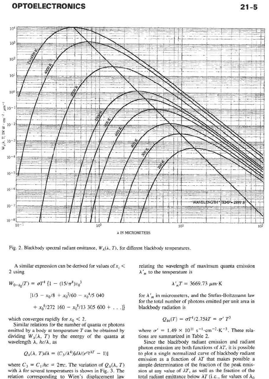
Blackbody Radiation
Any surface of a body with a temperature greater than
absolute zero
(T
=
0
K) is a source of radiation. The
term “blackbody” applies to a thermal radiator that
absorbs completely all incident electromagnetic radia-
tion regardless of the wavelength, the direction of
incidence, or the polarization. Such a radiator also has
the maximum emission possible for any wavelength and
in any .direction for a thermal radiator in thermal
equilibrium at a given temperature. Kirchhoffs law
states that for any body (all materials) in an isothermal
enclosure at temperature
T,
the ratio of the radiant
excitance (emittance),
W,
to
the absorptance,
a,
is
equal
to
the radiant excitance of a blackbody,
Wbb,
at
the same temperature:
W(T)/a
=
wbb(T)
Planck’s law gives the blackbody spectral power for
unpolarized radiation emitted at temperature
T
between
the wavelengths
A
and
A
+
dA
as
WA(A, T)dA
=
2m2hhm5
(ehclAkT
-
l)-’
dA
=
CldA/A5(eC2’AT
-
1)
where,
k
=
1.38
X
J-K-l is Boltzmann’s
C,
=
2nc2h
=
3.74
x
lo4
W.~m-~.pm~,
C2
=
ch/k
=
1.44
x
lo4
pm.K.
Fig.
2
shows the variation of
WA(A,
T)
with
A
for
various values
of
T.
The integral
of
WA(A,
T)dA
over
all
constant,
wavelengths gives the Stefan-Boltzmann law for total
blackbody radiant excitance
wbb(T)
in W/cm2,
wbb(T)
=
Wn(h,
T)dA
=
(2r5k4/15c2h3)T4
=
(T4C1/15C*4)T4
=
UT4
where
a
=
5.67
X
W.C~-~.K-~ is the Stefan-
Boltzmann constant. The blackbody spectrum has a
pronounced maximum at a particular wavelength
A,
for
a given temperature
T,
and the relationship
A,T
=
C2/4.9651
=
2897.8
pm*K
is known as Wien’s displacement law.
Planck’s law can also be specified in terms of
frequency or wave number instead of wavelength, and
these relations result in slightly different forms of
Wien’s displacement law.
For
calculations it is often
convenient to use the dimensionless quantity
x
=
hc/AkT
=
hv/kT
=
CZ/AT
for which Planck’s law becomes
WJx, T)dx
=
(15uT4/a4)[x3dn/(ex
-
l)]
The energy flux per unit area for wavelengths lying
between
x,
and
x2
can easily be calculated using the
series expansions below:
=
(15aT4/r4) x3dx/(e”
-
1)
where
=
hc/AokT
=
C2/A,T
and the energy flux per unit area for wavelengths
between
A2
and
A,
is given by
WhA
=
(15aT4/n4)
2
(~“/n~)[(nx)~
+
3(n~)~
+
6nx
+
61
1
n=l
x2
for
xi
2
2.
TABLE
1.
COMMON
RADIOMETRIC
TERMINOLOGY
N
4
Equation
h
Symbol Term Description Units
U
Radiant Energy transferred by
energy electromagnetic waves
J
U
Radiant energy Radiant energy per unit
density volume
J.c~-~
u
=
dUidV
radiant energy
W
P
=
dUidt
P
Radiant flux Rate of transfer
of
W
Radiant
Radiant flux emitted per
W
=
dPidA
emittance unit area
of
a source W.cm-2
Number of photons emitted
emittance
per second per unit area
intensity solid angle W.sr-l
J
=
dPidQ
Radiant photon
Phot0ns.s-'
aK2
Q
J
Radiant
Radiant flux per unit
N
Radiance Radiant flux per unit
H
Irradiance
Radiant flux incident per
solid angle per unit area W.cm-2.sr-'
N
=
Wiw
unit area W.cm-'
length interval at a particular
wavelength W.pm-'
PA
=
dPldA
H
=
dPidA
Spectral radiant
Radiant flux per unit wave-
PA
flux
n
rn
n
particular wavelength W.cm
-'
.pm
-I
WA
=
dWidA
rn
QA
Spectral radiant Radiant photon emittance per
n
photon emittance unit wavelength interval at a
rn
particular wavelength Photons.s-'.cm-'.pm-'
QA
=
dQidA
2
Spectral radiant Radiant intensity per unit wave-
c)
rn
JA
0
NA
NA
=
dNidA
P
Spectral Irradiance per unit wavelength
HA
interval at a particular wave-
e
(Radiant) Ratio
of
radiant emittance of a
WA
Spectral radiant Radiant emittance per unit
emittance wavelength interval at a
intensity
length interval at a particular
wavelength W.sr-'.pm-'
JA
=
didA
interval at a particular
s
6
s
Spectral radiance
Radiance per unit wavelength
wavelength
W.cm
-2.
sr
-
I
.
pm
-
I
irradiance
n
c)
2
rn
reflectance to incident radiant flux (Numeric)
rn
7
(Radiant) Ratio
of
transmitted radiant
n
transmittance flux to incident radiant
flux
(Numeric)
v)
length Wxm-2.pm-'
HA
=
dHidA
emissivity
source to that of a blackbody at
the same temperature (Numeric)
absorptance to incident radiant flux (Numeric)
I
(Y
(Radiant) Ratio
of
absorbed radiant flux
e
(Radiant)
Ratio
of
reflected radiant
flux
OPTOELECTRONICS
21
-5
103
102
101
100
*
g
10-
1
g
z
F
*-
10-3
10-4
N
1
s
10-2
-
k2
10-5
10-6
10-7
10-8
10-
1
100
10'
102
A
IN MICROMETERS
Fig.
2.
Blackbody spectral radiant emittance,
WA(h,
T),
for different blackbody temperatures.
A
similar expression can be derived for values of
xi
<
2
using
Wo-Ao(T)
=
uT4
(1
-
(15/,rr4)x2
[1/3
-
xo/S
+
~:/60
-
~0415
040
+
x2/272 160
-
x2/13 305 600
+
. .
.I}
which converges rapidly
for
xo
<
2.
Similar relations for the number of quanta or photons
emitted by a body at temperature
T
can be obtained by
dividing
WA(A,
T)
by the energy of the quanta at
wavelength
A,
hclh,
as
QA(A,
T)dA
=
(C3/A4)[dA/(eC2'AT
-
l)]
where
C3
=
Cl/hc
=
271~.
The variation of
QA(A,
T)
with
A
for several temperatures is shown in Fig.
3.
The
relation corresponding to Wien's displacement law
relating the wavelength of maximum quanta emission
A',
to the temperature is
A',T
=
3669.73
pm.K
for
A',
in micrometers, and the Stefan-Boltzmann law
for the total number of photons emitted per unit area in
blackbody radiation is
Qbb(T)
=
(rT4/2.75kT
=
LT'
T3
where
LT'
=
1.49
X
10" ~-'.cm-*.K-~. These rela-
tions are summarized in Table
2.
Since the blackbody radiant emission and radiant
photon emission are both functions of
AT,
it is possible
to plot a single normalized curve of blackbody radiant
emission as a function of
AT
that makes possible a
simple determination of the fraction
of
the peak emis-
sion at any value of
AT,
as well as the fraction of the
total radiant emittance below
AT
(Le., for values of
A0