Neamen D. Microelectronics: Circuit Analysis and Design
Подождите немного. Документ загружается.

278 Part 1 Semiconductor Devices and Basic Applications
4.58 For the source-follower circuit with a saturated load as shown in Fig-
ure P4.57, assume the same transistor parameters as given in Problem 4.57.
(a) Determine the small-signal voltage gain if
R
L
= 10
k
. (b) Determine
the small-signal output resistance R
o
.
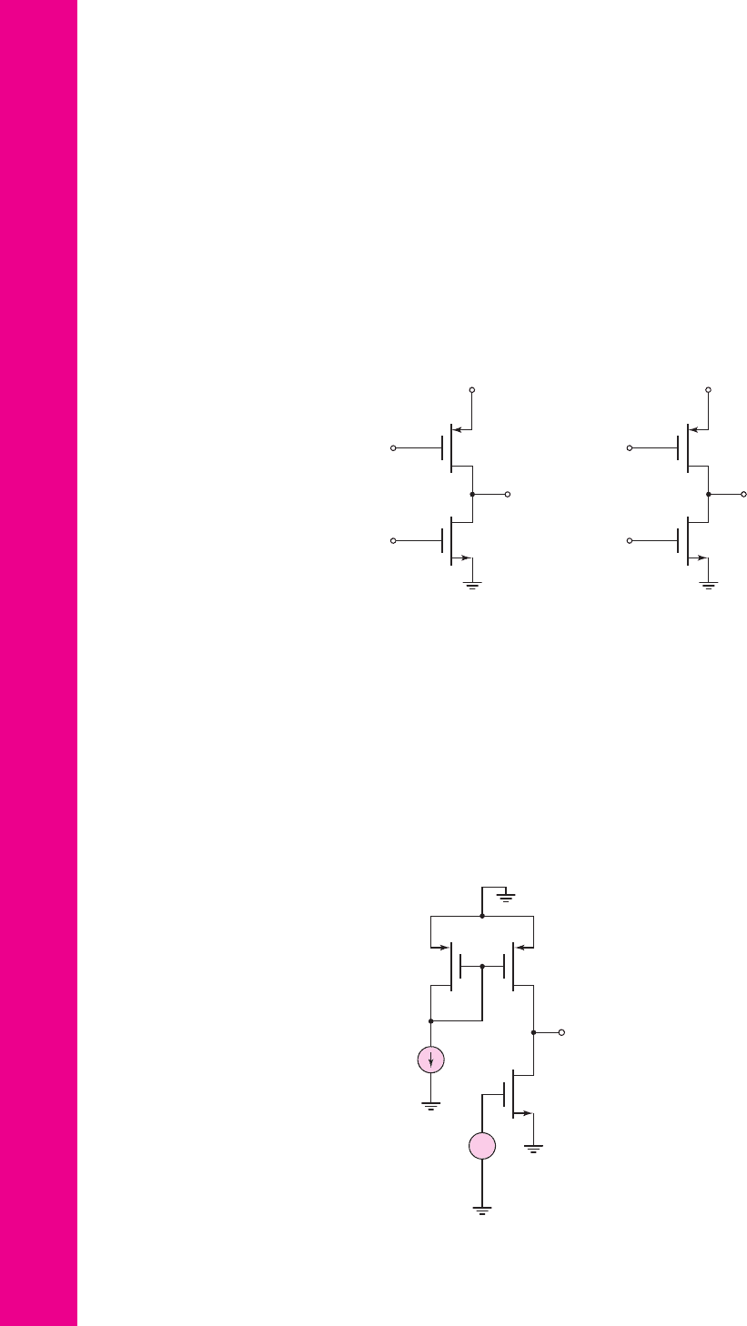
4.59 The transistor parameters for the common-source circuit in Figure P4.59
are
V
TND
= 0.4
V,
V
TPL
=−0.4
V,
(
W/L
)
L
= 50
,
λ
D
= 0.02
V
−1
,
λ
L
= 0.04
V
−1
,
k
n
= 100 μ
A/V
2
, and
k
p
= 40 μ
A/V
2
. At the Q-point,
I
DQ
= 0.5
mA. (a) Determine
(
W/L
)
D
such that the small-signal voltage
gain is
A
v
= V
o
/V
i
=−40
. (b) What is the required value of
V
B
? (c) What
is the value of
V
GSDQ
?
V
B
M
L
M
D
V
o
V
i
V
+
= 2.5 V
Figure P4.59
V
i
M
D
M
L
V
o
V
B
V
+
= 2.5 V
Figure P4.60
+
–
M
3
M
2
M
1
v
o
v
i
I
Q
=
100 mA
Figure P4.61
4.60 Consider the circuit in Figure P4.60. The transistor parameters are
V
TPD
=−0.6
V,
V
TNL
= 0.4
V,
k
n
= 100 μ
A/V
2
,
k
p
= 40 μ
A/V
2
,
λ
L
= 0.02
V
−1
,
λ
D
= 0.04
V
−1
, and
(
W/L
)
L
= 10
. (a) At the
Q
-point, the
quiescent drain current is
I
DQ
= 0.25
mA. (i) Determine
(
W/L
)
D
such that
the small-signal voltage gain is
A
v
= V
o
/V
i
=−25
. (ii) What is the re-
quired value of
V
B
? (iii) What is the value of
V
SGDQ
? (b) Repeat part (a) for
I
DQ
= 0.1
mA.
4.61 The ac equivalent circuit of a CMOS common-source amplifier is shown in
Figure P4.61. The transistor parameters for M
1
are
V
TN
= 0.5
V,
k
n
=
85 μA/V
2
,
(W/L)
1
= 50
, and
λ = 0.05 V
−1
, and for M
2
and M
3
are
nea80644_ch04_205-284.qxd 06/12/2009 08:00 PM Page 278 F506 Tempwork:Dont' Del Rakesh:June:Rakesh 06-12-09:MHDQ134-04:
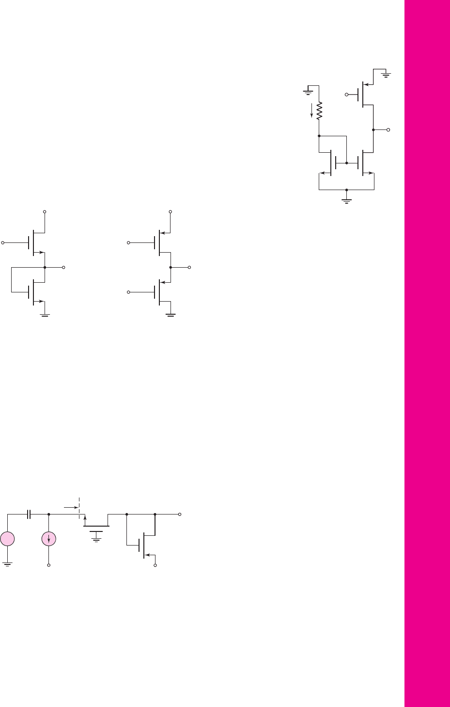
Chapter 4 Basic FET Amplifiers 279
V
TP
=−0.5V
,
k
p
= 40 μA/V
2
,
(W/L)
2,3
= 50
, and
λ = 0.075 V
−1
.
Determine the small-signal voltage gain.
4.62 Consider the ac equivalent circuit of a CMOS common-source amplifier shown
in Figure P4.62. The parameters of the NMOS and PMOS transistors are the
same as given in Problem 4.61. Determine the small-signal voltage gain.
4.63 The parameters of the transistors in the circuit in Figure P4.63 are
V
TND
=
V
TNL
= 0.4
V,
K
nD
= 2
mA/V
2
,
K
nL
= 0.5
mA/V
2
, and
λ
D
= λ
L
= 0
.
(a) Plot
V
o
versus
V
I
over the range
0.8 ≤ V
I
≤ 2.5
V. (b) Plot
I
D
versus
V
I
over the same voltage range as part (a). (c) At
I
DQ
= 0.20
mA, find the small-
signal voltage gain
A
v
= V
o
/V
i
= dV
O
/dV
I
.
+
–
R
i
V
i
I
Q
=
1 mA
V
+
= 3.3 V
V
–
= –3.3 V
V
o
M
L
M
D
C
C
Figure P4.65
4.64 Consider the source-follower circuit in Figure P4.64. The transistor para-
meters are
V
TP
=−0.4
V,
k
p
= 40 μ
A/V
2
,
(
W/L
)
L
= 5
,
(
W/L
)
D
= 50
,
and
λ
D
= λ
L
= 0.025
V
−1
. Assume
V
B
= 1
V. (a) What is the maximum
value of
V
o
such that
M
L
remains biased in the saturation region? (b) For
M
L
biased in the saturation region, determine
I
D
. (c) Using the results of
parts (a) and (b), find
V
SGD
. (d) Determine the small-signal voltage gain
when the dc value of
V
I
= 0.2
V.
4.65 Figure P4.65 shows a common-gate amplifier. The transistor parameters
are
V
TN
= 0.6
V,
V
TP
=−0.6
V,
K
n
= 2mA/V
2
,
K
p
= 0.5
mA/V
2
, and
λ
n
= λ
p
= 0
. (a) Find the values of
V
SGLQ
,
V
GSDQ
, and
V
DSDQ
. (b) Derive
the expression for the small-signal voltage gain in terms of
K
n
and
K
p
.
(c) Calculate the value of the small-signal voltage gain
A
v
= V
o
/V
i
.
V
I
M
D
M
L
V
o
V
+
= 2.5 V
Figure P4.63
V
B
M
L
M
D
V
I
V
+
= 2.5 V
V
o
Figure P4.64
4.66 The ac equivalent circuit of a CMOS common-gate circuit is shown in Fig-
ure P4.66. The parameters of the NMOS and PMOS transistors are the same
as given in Problem 4.61. Determine the (a) small-signal parameters of the
transistors, (b) small-signal voltage gain
A
v
= v
o
/v
i
, (c) input resistance R
i
,
and (d) output resistance R
o
.
M
3
M
2
R
I
REF
=
100 mA
M
1
v
o
v
i
Figure P4.62
nea80644_ch04_205-284.qxd 06/12/2009 08:00 PM Page 279 F506 Tempwork:Dont' Del Rakesh:June:Rakesh 06-12-09:MHDQ134-04:
280 Part 1 Semiconductor Devices and Basic Applications
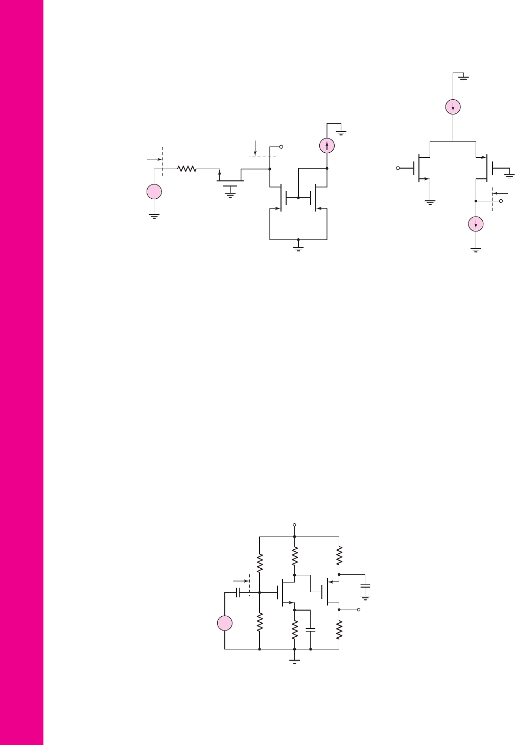
4.67 The circuit in Figure P4.67 is a simplified ac equivalent circuit of a folded-
cascode amplifier. The transistor parameters are
|
V
TN
|
=
|
V
TP
|
= 0.5V
,
K
n
= K
p
= 2
mA/V
2
, and
λ
n
= λ
p
= 0.1V
−1
. Assume the current source
2I
Q
= 200 μ
A is ideal and the resistance looking into the current
source
I
Q
= 100 μ
A is 50 k
. Determine the (a) small-signal parameters of
each transistor, (b) small-signal voltage gain, and (c) output resistance R
o
.
Section 4.8 Multistage Amplifiers
4.68 The transistor parameters in the circuit in Figure P4.68 are
V
TN1
= 0.6
V,
V
TP2
=−0.6
V,
K
n1
= 0.2
mA/V
2
,
K
p2
= 1.0
mA/V
2
, and
λ
1
= λ
2
= 0
.
The circuit parameters are
V
DD
= 5
V and
R
in
= 400 k
. (a) Design the
circuit such that
I
DQ1
= 0.2
mA,
I
DQ2
= 0.5
mA,
V
DSQ1
= 2
V, and
V
SDQ2
= 3
V. The voltage across
R
S1
is to be 0.6 V. (b) Determine the
small-signal voltage gain
A
v
= v
o
/v
i
.
I
Q
=
100 mA
2I
Q
=
200 mA
M
2
M
1
R
o
v
o
v
i
Figure P4.67
+
–
50 Ω
M
1
I
Q
=
100 m
A
M
2
R
i
R
o
v
o
v
i
M
3
Figure P4.66
v
i
C
C
v
O
R
2
R
in
R
1
R
D1
R
D2
R
S1
C
S1
C
S2
V
DD
M
2
M
1
R
S2
+
–
Figure P4.68
nea80644_ch04_205-284.qxd 06/12/2009 08:00 PM Page 280 F506 Tempwork:Dont' Del Rakesh:June:Rakesh 06-12-09:MHDQ134-04:
Chapter 4 Basic FET Amplifiers 281
4.69 The transistor parameters in the circuit in Figure P4.68 are the same as those
given in Problem 4.68. The circuit parameters are
V
DD
= 3.3
V,
R
S1
= 1
k
, and
R
in
= 250
k
. (a) Design the circuit such that
I
DQ1
= 0.1
mA,
I
DQ2
= 0.25
mA,
V
DSQ1
= 1.2
V, and
V
SDQ2
= 1.8
V.
(b) Determine the small-signal voltage gain
A
v
= v
o
/v
i
.
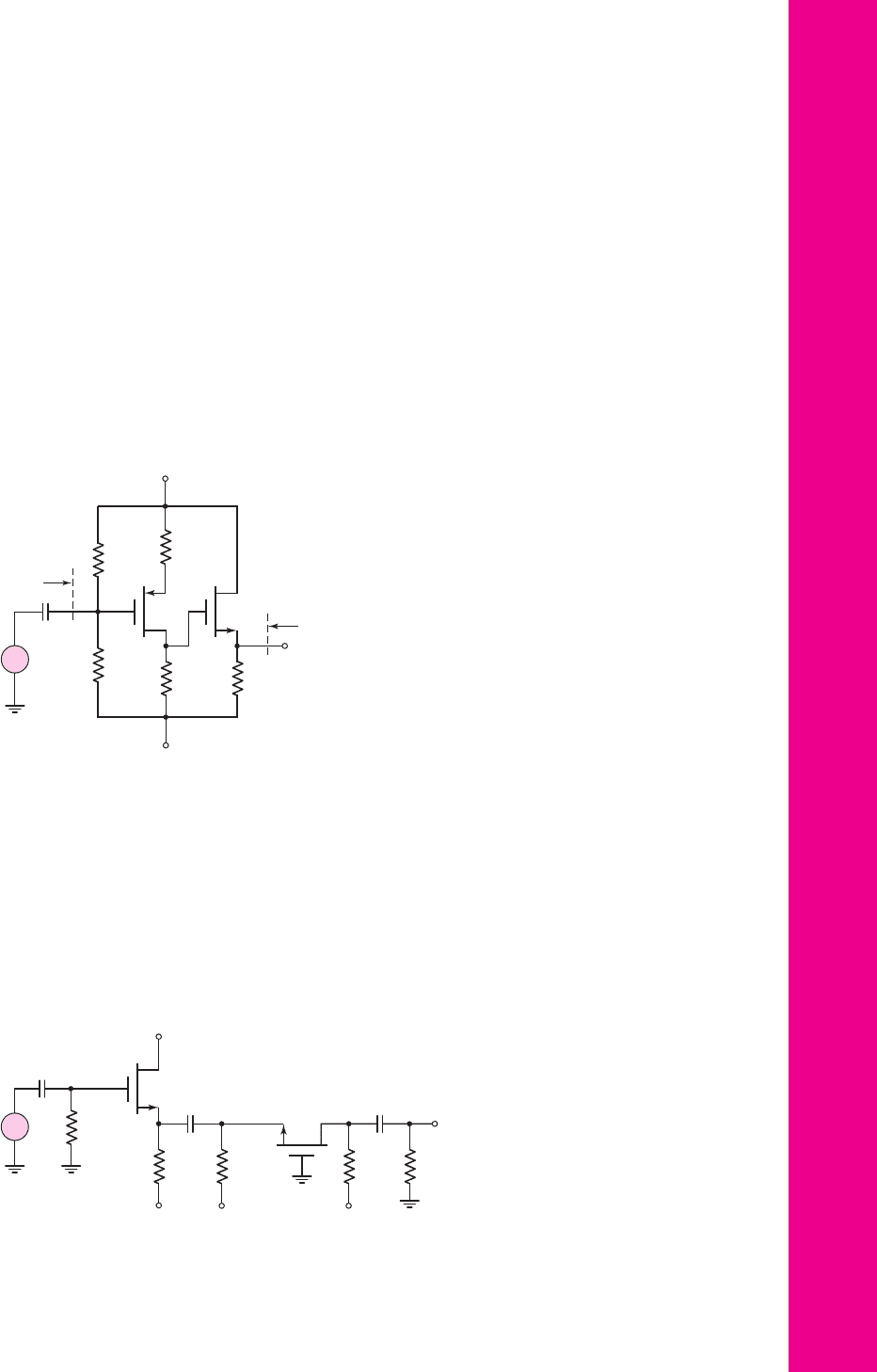
4.70 Consider the circuit shown in Figure P4.70. The transistor parameters
are
V
TP1
=−0.4
V,
V
TN2
= 0.4
V,
(
W/L
)
1
= 20
,
(
W/L
)
2
= 80
,
k
p
= 40 μ
A/V
2
,
k
n
= 100 μ
A/V
2
, and
λ
1
= λ
2
= 0
. Let
R
in
= 200
k
. (a)
Design the circuit such that
I
DQ1
= 0.1
mA,
I
DQ2
= 0.3
mA,
V
SDQ1
= 1.0
V, and
V
DSQ2
= 2.0
V. The voltage across
R
S1
is to be 0.6 V.
(b) Determine the small-signal voltage gain
A
v
= v
o
/v
i
. (c) Find the small-
signal output resistance
R
o
.
4.71 For the circuit in Figure P4.71, the transistor parameters are:
K
n1
=
K
n2
= 4
mA/V
2
,
V
TN1
= V
TN2
= 2
V, and
λ
1
= λ
2
= 0
. (a) Determine
I
DQ1
,
I
DQ2
,
V
DSQ1
, and
V
DSQ2
. (b) Determine
g
m1
and
g
m2
. (c) Deter-
mine the overall small-signal voltage gain
A
v
= v
o
/v
i
.
+
–
C
C
R
1
M
1
M
2
R
2
R
D1
R
S1
R
S2
v
i
V
+
= 1.8 V
V
–
= –1.8 V
R
in
v
o
R
o
Figure P4.70
C
C2
C
C3
v
o
R
S1
=
10 kΩ
R
S2
=
10 kΩ
R
D
=
5 kΩ
R
L
=
2 kΩ
+10 V
10 V
–10 V –10 V
v
i
R
G
=
400 kΩ
C
C1
M
2
M
1
+
–
Figure P4.71
nea80644_ch04_205-284.qxd 06/12/2009 08:00 PM Page 281 F506 Tempwork:Dont' Del Rakesh:June:Rakesh 06-12-09:MHDQ134-04:
282 Part 1 Semiconductor Devices and Basic Applications
D4.72 For the cascode circuit in Figure 4.51 in the text, the transistor parameters
are:
V
TN1
= V
TN2
= 1
V,
K
n1
= K
n2
= 2
mA/V
2
, and
λ
1
= λ
2
= 0
. (a) Let
R
S
= 1.2
k
and
R
1
+ R
2
+ R
3
= 500
k
. Design the circuit such that
I
DQ
= 3
mA and
V
DSQ1
= V
DSQ2
= 2.5
V. (b) Determine the small-signal
voltage gain
A
v
= v
o
/v
i
.
D4.73 The supply voltages to the cascode circuit in Figure 4.51 in the text are
changed to
V
+
= 10
V and
V
−
=−10 V
. The transistor parameters are:
K
n1
= K
n2
= 4
mA/V
2
,
V
TN1
= V
TN2
= 1.5
V, and
λ
1
= λ
2
= 0
. (a) Let
R
S
= 2
k
, and assume the current in the bias resistors is 0.1 mA. Design
the circuit such that
I
DQ
= 5
mA and
V
DSQ1
= V
DSQ2
= 3.5
V. (b) Deter-
mine the resulting small-signal voltage gain.
Section 4.9 Basic JFET Amplifiers
4.74 Consider the JFET amplifier in Figure 4.53 with transistor parameters
I
DSS
= 6
mA,
V
P
=−3V
, and
λ = 0.01 V
−1
. Let
V
DD
= 10
V. (a) Deter-
mine R
D
and V
GS
such that
I
DQ
= 4
mA and
V
DSQ
= 6
V. (b) Determine
g
m
and
r
o
at the Q-point. (c) Determine the small-signal voltage gain
A
v
= v
o
/v
i
where
v
o
is the time-varying portion of the output voltage
v
O
.
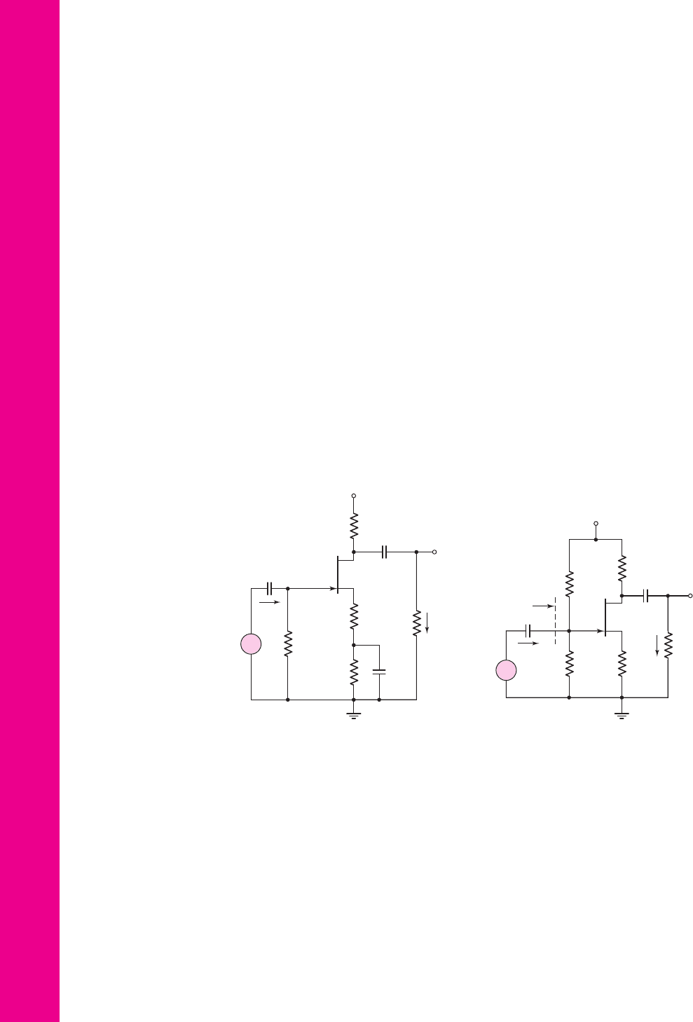
4.75 For the JFET amplifier in Figure P4.75, the transistor parameters are:
I
DSS
= 2
mA,
V
P
=−2V
,and
λ = 0
. Determine
g
m
,
A
v
= v
o
/v
i
, and
A
i
= i
o
/i
i
.
v
i
C
C
R
D
= 8 kΩ
V
DD
v
o
R
S2
=
250 Ω
R
G
=
50 k Ω
R
S1
=
100 Ω
R
L
=
4 k Ω
C
C2
C
S
i
i
i
o
+
–
Figure P4.75
v
i
C
C1
R
in
v
o
R
L
R
S
R
D
R
1
R
2
C
C2
V
DD
i
i
i
o
+
–
Figure P4.76
D4.76 The parameters of the transistor in the JFET common-source amplifier
shown in Figure P4.76 are:
I
DSS
= 8
mA,
V
P
=−4.2V
, and
λ = 0
. Let
V
DD
= 20
V and
R
L
= 16
k
. Design the circuit such that
V
S
= 2
V,
R
1
+ R
2
= 100
k
, and the Q-point is at
I
DQ
= I
DSS
/2
and
V
DSQ
=
V
DD
/2
.
*D4.77 Consider the source-follower JFET amplifier in Figure P4.77 with transistor
parameters
I
DSS
= 10
mA,
V
P
=−5V
, and
λ = 0.01 V
−1
. Let
V
DD
= 12
V
and
R
L
= 0.5
k
. (a) Design the circuit such that
R
in
= 100
k
, and the
Q-point is at
I
DQ
= I
DSS
/2
and
V
DSQ
= V
DD
/2
. (b) Determine the result-
ing small-signal voltage gain
A
v
= v
o
/v
i
and the output resistance
R
o
.
nea80644_ch04_205-284.qxd 06/12/2009 08:00 PM Page 282 F506 Tempwork:Dont' Del Rakesh:June:Rakesh 06-12-09:MHDQ134-04:
4.78 For the p-channel JFET source-follower circuit in Figure P4.78, the transis-
tor parameters are:
I
DSS
= 2
mA,
V
P
=+1.75
V, and
λ = 0
. (a) Determine
I
DQ
and
V
SDQ
. (b) Determine the small-signal gains
A
v
= v
o
/v
i
and
A
i
=
i
o
/i
i
. (c) Determine the maximum symmetrical swing in the output voltage.
D4.79 The p-channel JFET common-source amplifier in Figure P4.79 has transis-
tor parameters
I
DSS
= 8
mA,
V
P
= 4
V, and
λ = 0
. Design the circuit
such that
I
DQ
= 4
mA,
V
SDQ
= 7.5
V,
A
v
= v
o
/v
i
=−3
, and
R
1
+ R
2
=
400 k
.
Chapter 4 Basic FET Amplifiers 283
v
i
C
C1
R
in
v
o
R
L
R
2
R
S
R
1
C
C 2
V
DD
i
i
i
o
R
o
+
–
Figure P4.77
v
i
v
o
R
2
= 110 kΩ
R
1
= 90 kΩ
R
L
=
10 kΩ
R
S
= 5 kΩ
C
C2
C
C1
V
DD
= 10 V
i
i
i
o
+
–
Figure P4.78
v
i
C
C1
v
O
R
2
R
1
R
D
R
S
V
DD
= 20 V
+
–
Figure P4.79
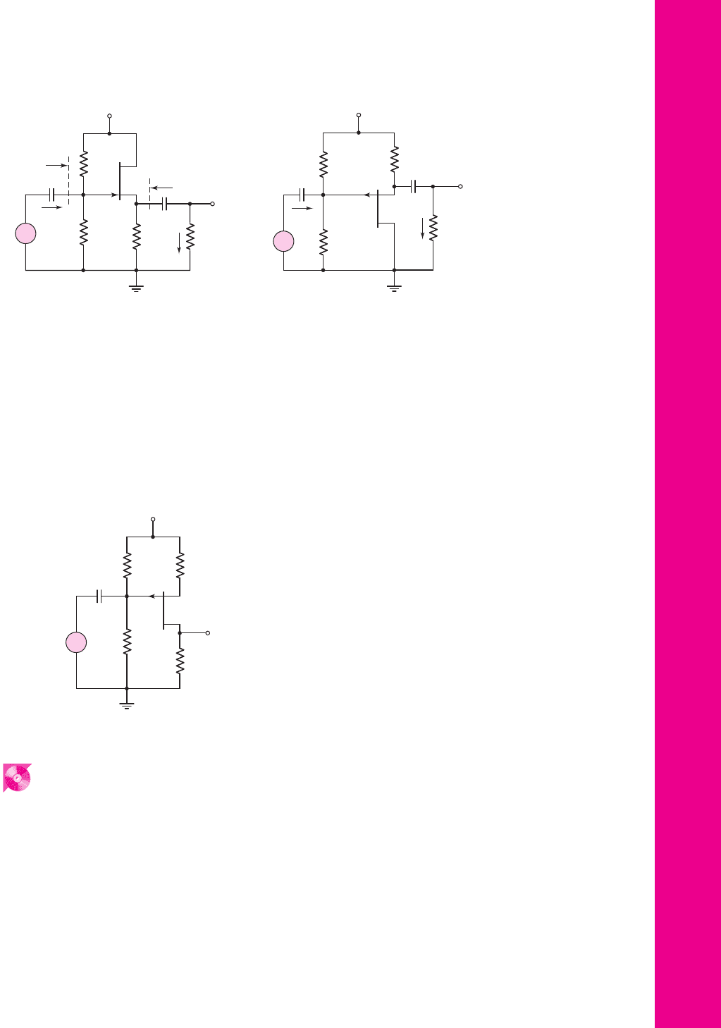
COMPUTER SIMULATION PROBLEMS
4.80 Consider the common-source circuit described in Example 4.5. (a) Using a
computer simulation, verify the results obtained in Example 4.5. (b) Deter-
mine the change in the results when the body effect is taken into account.
4.81 Using a computer simulation, verify the results of Example 4.7 for the
source-follower amplifier.
4.82 Using a computer simulation, verify the results of Example 4.10 for the
common-gate amplifier.
4.83 Using a computer simulation, verify the results of Example 4.17 for the cas-
code amplifier.
nea80644_ch04_205-284.qxd 06/12/2009 08:01 PM Page 283 F506 Tempwork:Dont' Del Rakesh:June:Rakesh 06-12-09:MHDQ134-04:

DESIGN PROBLEMS
[Note: Each design should be correlated with a computer analysis.]
*D4.84 A discrete common-source circuit with the configuration shown in Figure
4.17 is to be designed to provide a voltage gain of 18 and a symmetrical out-
put voltage swing. The bias voltage is
V
DD
= 3.3
V, the output resistance of
the signal source is
500
, and the transistor parameters are:
V
TN
= 0.4V
,
k
n
= 100 μ
A/V
2
, and
λ = 0.01
V
−1
. Assume a quiescent drain current of
I
DQ
= 100 μ
A.
*D4.85 Consider the common-gate amplifier shown in Figure 4.35. The power supply
voltages are
±5
V, the output resistance of the signal source is
500
, and the
input resistance of the amplifier is to be
200
. The transistor parameters are
k
p
= 40 μ
A/V
2
,
V
TP
=−0.6
V, and
λ = 0
. The output load resistance is
R
L
= 10
k
. Design the circuit such that the output voltage has a peak-
to-peak symmetrical swing of at least 4 V.
*D4.86 A source-follower amplifier with the configuration shown in Figure 4.31 is
to be designed. The power supplies are to be
±12
V. The transistor parame-
ters are
V
TN
= 1.2
V,
k
n
= 100 μ
A/V
2
, and
λ = 0
. The load resistance is
R
L
= 200
. Design the circuit, as well as a constant-current source, to de-
liver 250 mW of signal power to the load.
*D4.87 Consider the multitransistor circuit in Figure 4.49. Assume transistor para-
meters of
V
TN
= 0.6
V,
k
n
= 100 μ
A/V
2
, and
λ = 0
. Design the transistors
such that the small-signal voltage gain of the first stage is
A
v1
=−10
and
the small-signal voltage gain of the second stage is
A
v2
= 0.9
.
284 Part 1 Semiconductor Devices and Basic Applications
nea80644_ch04_205-284.qxd 06/13/2009 01:56 PM Page 284 F506 Hard disk:Desktop Folder:ALI-06-13-09:MHDQ134-04 Folder:MHDQ134-0

Chapter
The Bipolar
Junction Transistor
5
5
285
In Chapter 2, we saw that the rectifying current–voltage characteristics of the diode
are useful in electronic switching and waveshaping circuits. However, diodes are not
capable of amplifying currents or voltages. As was shown in Chapter 4, the electronic
device that is capable of current and voltage amplification, or gain, in conjunction
with other circuit elements, is the transistor. The development of the transistor by
Bardeen, Brattain, and Schockley at Bell Telephone Laboratories in the late 1940s
started the first electronics revolution of the 1950s and 1960s. This invention led to
the development of the first integrated circuit in 1958 and to the transistor operational
amplifier (op-amp), which is one of the most widely used electronic circuits.
The bipolar transistor, which is introduced in this chapter, is one of the two
major types of transistors. The second type of transistor, the field-effect transistor
(FET), was introduced in Chapter 3. These two device types are the basis of modern
microelectronics. Each device type is equally important and each has particular ad-
vantages for specific applications.
PREVIEW
In this chapter, we will:
• Discuss the physical structure and operation of the bipolar junction transistor.
• Understand and become familiar with the dc analysis and design techniques
of bipolar transistor circuits.
• Examine three basic applications of bipolar transistor circuits.
• Investigate various dc biasing schemes of bipolar transistor circuits, includ-
ing integrated circuit biasing.
• Consider the dc biasing of multistage or multi-transistor circuits.
• As an application, incorporate the bipolar transistor in a circuit design that
enhances the simple diode electronic thermometer discussed in Chapter 1.
nea80644_ch05_285-368.qxd 06/12/2009 08:42 PM Page 285 F506 Tempwork:Dont' Del Rakesh:June:Rakesh 06-12-09:MHDQ134-05:

Collector
Base
Emitter
p
p
(b)
(a)
Collector
Base
Emitter
p
nn
n
Figure 5.1 Simple geometry of bipolar transistors: (a) npn and (b) pnp
286 Part 1 Semiconductor Devices and Basic Applications
5.1 BASIC BIPOLAR JUNCTION TRANSISTOR
Objective: • Understand the physical structure, operation, and char-
acteristics of the bipolar junction transistors (BJT), including the npn
and pnp devices.
The bipolar junction transistor (BJT) has three separately doped regions and con-
tains two pn junctions.A single pn junction has two modes of operation—forward bias
and reverse bias. The bipolar transistor, with two pn junctions, therefore has four pos-
sible modes of operation, depending on the bias condition of each pn junction, which
is one reason for the versatility of the device. With three separately doped regions, the
bipolar transistor is a three-terminal device. The basic transistor principle is that
the voltage between two terminals controls the current through the third terminal.
Our discussion of the bipolar transistor starts with a description of the basic tran-
sistor structure and a qualitative description of its operation. To describe its operation,
we use the pn junction concepts presented in Chapter 1. However, the two pn junctions
are sufficiently close together to be called interacting pn junctions. The operation of
the transistor is therefore totally different from that of two back-to-back diodes.
Current in the transistor is due to the flow of both electrons and holes, hence the
name bipolar. Our discussion covers the relationship between the three terminal cur-
rents. In addition, we present the circuit symbols and conventions used in bipolar
circuits, the bipolar transistor current–voltage characteristics, and finally, some non-
ideal current–voltage characteristics.
Transistor Structures
Figure 5.1 shows simplified block diagrams of the basic structure of the two types of
bipolar transistor: npn and pnp. The npn bipolar transistor contains a thin p-region
between two n-regions. In contrast, the pnp bipolar transistor contains a thin n-
region sandwiched between two p-regions. The three regions and their terminal
connections are called the emitter, base, and collector.
1
The operation of the device
depends on the two pn junctions being in close proximity, so the width of the base
must be very narrow, normally in the range of tenths of a micrometer
(10
−6
m)
.
The actual structure of the bipolar transistor is considerably more complicated
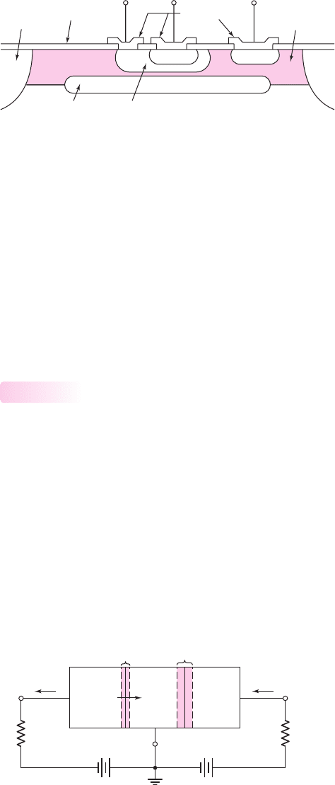
than the block diagrams of Figure 5.1. For example, Figure 5.2 is the cross section of
5.1.1
1
The reason for the names emitter and collector for the terminals will become obvious as we go through
the operation of the transistor. The term base refers to the structure of the original transistor.
nea80644_ch05_285-368.qxd 06/12/2009 08:42 PM Page 286 F506 Tempwork:Dont' Del Rakesh:June:Rakesh 06-12-09:MHDQ134-05:
Chapter 5 The Bipolar Junction Transistor 287
a classic npn bipolar transistor fabricated in an integrated circuit. One important
point is that the device is not symmetrical electrically. This asymmetry occurs
because the geometries of the emitter and collector regions are not the same, and the
impurity doping concentrations in the three regions are substantially different. For
example, the impurity doping concentrations in the emitter, base, and collector may
be on the order of 10
19
,10
17
, and 10
15
cm
−3
, respectively. Therefore, even though
both ends are either p-type or n-type on a given transistor, switching the two ends
makes the device act in drastically different ways.
Although the block diagrams in Figure 5.1 are highly simplified, they are still
useful for presenting the basic transistor characteristics.
npn Transistor: Forward-Active Mode Operation
Since the transistor has two pn junctions, four possible bias combinations may be ap-
plied to the device, depending on whether a forward or reverse bias is applied to each
junction. For example, if the transistor is used as an amplifying device, the base–emitter
(B–E) junction is forward biased and the base–collector (B–C) junction is reverse
biased, in a configuration called the forward-active operating mode, or simply the
active region. The reason for this bias combination will be illustrated as we look at
the operation of such transistors and the characteristics of circuits that use them.
Transistor Currents
Figure 5.3 shows an idealized npn bipolar transistor biased in the forward-active mode.
Since the B–E junction is forward biased, electrons from the emitter are injected across
5.1.2
–
V
BB
+
–
V
BE
+
–
V
CC
+
CE
B
pnn
Electron
injection
Base-emitter
(B–E) junction
Base-collector
(B–C) junction
R
C
R
E
i
E
i
C
Figure 5.3 An npn bipolar transistor biased in the forward-active mode; base–emitter
junction forward biased and base–collector junction reverse biased
Isolation
Aluminum
Epitaxial
layer
Silicon
substrate
Base
Buried
layer
p
+
p
p
+
p
+
n
++
n
++
n
++
n
SiO
2
BE C
Figure 5.2 Cross section of a conventional integrated circuit npn bipolar transistor
nea80644_ch05_285-368.qxd 06/12/2009 08:42 PM Page 287 F506 Tempwork:Dont' Del Rakesh:June:Rakesh 06-12-09:MHDQ134-05: