Neamen D. Microelectronics: Circuit Analysis and Design
Подождите немного. Документ загружается.

298 Part 1 Semiconductor Devices and Basic Applications
–
V
CB
+
C
B
E
pn
n
–
V
CE
+
I
CBO
I
CEO
I
CBO
C
B
E
pn
n
α
I
CEO
(a) (b)
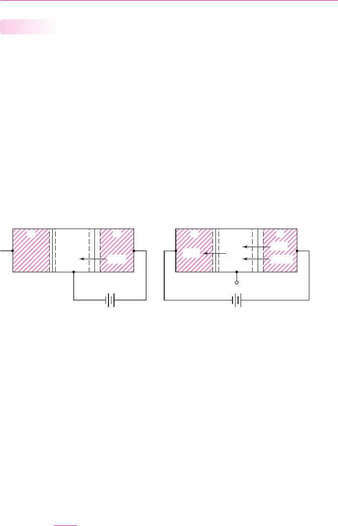
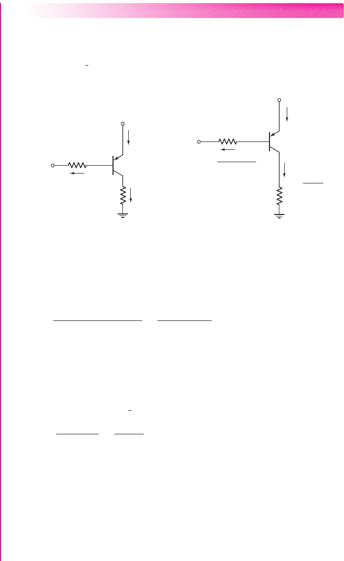
Figure 5.15 Block diagram of an npn transistor in an (a) open-emitter configuration showing
the junction leakage current
I
CBO
and (b) open-base configuration showing the leakage
current
I
CEO
TYU 5.5 Assume that
I
C
= 1
mA at
V
CE
= 1
V, and that
V
BE
is held constant.
Determine
I
C
at
V
CE
= 10
V if: (a)
V
A
= 75
V; and (b)
V
A
= 150
V. (Ans.
I
C
=
1.12 mA, 1.06 mA)
Nonideal Transistor Leakage Currents
and Breakdown Voltage
In discussing the current–voltage characteristics of the bipolar transistor in the previ-
ous sections, two topics were ignored: leakage currents in the reverse-biased pn junc-
tions and breakdown voltage effects.
Leakage Currents
In the common-base circuits in Figure 5.11, if we set the current source
i
E
= 0
, tran-
sistors will be cut off, but the B–C junctions will still be reverse biased. A reverse-
bias leakage current exists in these junctions, and this current corresponds to the
reverse-bias saturation current in a diode, as described in Chapter 1. The direction of
these reverse-bias leakage currents is the same as that of the collector currents. The
term
I
CBO
is the collector leakage current in the common-base configuration, and is
the collector-base leakage current when the emitter is an open circuit. This leakage
current is shown in Figure 5.15(a).
5.1.6
Another leakage current can exist between the emitter and collector with the
base terminal an open circuit. Figure 5.15(b) is a block diagram of an npn transistor
in which the base is an open circuit
(i
B
= 0)
. The current component
I
CBO
is the nor-
mal leakage current in the reverse-biased B–C pn junction. This current component
causes the base potential to increase, which forward biases the B–E junction and in-
duces the B–E current
I
CEO
. The current component
αI
CEO
is the normal collector
current resulting from the emitter current
I
CEO
. We can write
I
CEO
= α I
CEO
+ I
CBO
(5.19(a))
or
I
CEO
=
I
CBO
1 − α
∼
=
β I
CBO
(5.19(b))
This relationship indicates that the open-base configuration produces different char-
acteristics than the open-emitter configuration.
nea80644_ch05_285-368.qxd 06/12/2009 08:42 PM Page 298 F506 Tempwork:Dont' Del Rakesh:June:Rakesh 06-12-09:MHDQ134-05:
Chapter 5 The Bipolar Junction Transistor 299
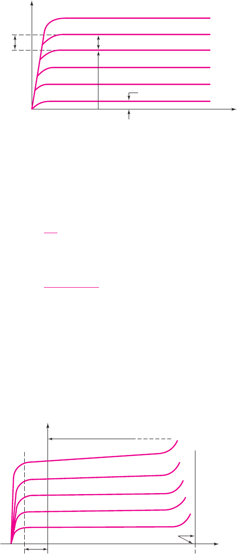
i
C
I
C2
I
B2
I
CBO
I
CEO
v
CE
ΔI
C
ΔI
B
Figure 5.16 Transistor current–voltage characteristics for the common-emitter circuit includ-
ing leakage currents. The dc beta and ac beta for the transistor can be determined from this set
of characteristics. The Early voltage for this set of characteristics is assumed to be
V
A
=∞
.
0
i
C
i
E
= I
E2
i
E
= I
E1
i
E
= 0
v
CB
BV
CBO
Forward-active mode
0.2–0.3 V
Figure 5.17 The
i
C
versus
v
CB
common-base characteristics, showing the collector–base
junction breakdown
When the transistor is biased in the forward-active mode, the various leakage
currents still exist. Common-emitter current–voltage characteristics are shown in
Figure 5.16, in which the leakage current has been included.A dc beta or dc common-
emitter current gain can be defined, for example, as
β
dc
=
I
C2
I
B2
(5.20)
where the collector current
I
C2
includes the leakage current as shown in the figure.
An ac
β
is defined as
β
ac
=
I
C
I
B|V
CE
=const.
(5.21)
This definition of beta excludes the leakage current as shown in the figure.
If the leakage currents are negligible, the two values of beta are equal. We will
assume in the remainder of this text that the leakage currents can be neglected and
beta can simply be denoted as
β
as previously defined.
Breakdown Voltage: Common-Base Characteristics
The common-base current–voltage characteristics shown in Figure 5.12 are ideal in
that breakdown is not shown. Figure 5.17 shows the same
i
C
versus
v
CB
character-
istics with the breakdown voltage.
nea80644_ch05_285-368.qxd 06/12/2009 08:42 PM Page 299 F506 Tempwork:Dont' Del Rakesh:June:Rakesh 06-12-09:MHDQ134-05:
300 Part 1 Semiconductor Devices and Basic Applications
Consider the curve for
i
E
= 0
(the emitter terminal is effectively an open cir-
cuit). The collector–base junction breakdown voltage is indicated as
BV
CBO
. This is
a simplified figure in that it shows breakdown occurring abruptly at
BV
CBO
. For the
curves in which
i
E
> 0
, breakdown actually begins earlier. The carriers flowing
across the junction initiate the breakdown avalanche process at somewhat lower
voltages.
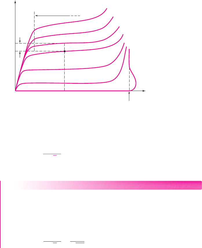
Breakdown Voltage: Common-Emitter Characteristics
Figure 5.18 shows the
i
C
versus
v
CE
characteristics of an npn transistor, for various
constant base currents, and an ideal breakdown voltage of
BV
CEO
. The value of
BV
CEO
is less than the value of
BV
CBO
because
BV
CEO
includes the effects of the
transistor action, while
BV
CBO
does not. This same effect was observed in the
I
CEO
leakage current.
v
C
E
BV
CEO
0
I
CQ
i
C
V
CEQ
i
B
=
…
i
B
= 0
i
B
= I
BQ
i
B
= I
B1
i
B
= I
B2
i
B
= I
BQ
+ Δi
B
Forward-active mode
Δi
C
Figure 5.18 Common-emitter characteristics showing breakdown effects
The breakdown voltage characteristics for the two configurations are also dif-
ferent. The breakdown voltage for the open-base case is given by
BV
CEO
=
BV
CBO
n
√
β
(5.22)
where n is an empirical constant usually in the range of 3 to 6.
EXAMPLE 5.2
Objective: Calculate the breakdown voltage of a transistor connected in the open-
base configuration.
Assume that the transistor current gain is
β = 100
and that the breakdown volt-
age of the B–C junction is
BV
CBO
= 120
V.
Solution: If we assume an empirical constant of
n = 3
, we have
BV
CEO
=
BV
CBO
n
√
β
=
120
3
√
100
= 25.9V
nea80644_ch05_285-368.qxd 06/12/2009 08:42 PM Page 300 F506 Tempwork:Dont' Del Rakesh:June:Rakesh 06-12-09:MHDQ134-05:

Chapter 5 The Bipolar Junction Transistor 301
Comment: The breakdown voltage of the open-base configuration is substantially
less than that of the C–B junction. This represents a worst-case condition, which
must be considered in any circuit design.
Design Pointer: The designer must be aware of the breakdown voltage of the spe-
cific transistors used in a circuit, since this will be a limiting factor in the size of the
dc bias voltages that can be used.
EXERCISE PROBLEM
Ex 5.2: The open-emitter breakdown voltage is
BV
CBO
= 200
V, the current
gain is
β = 120
, and the empirical constant is
n = 3
. Determine
BV
CEO
.
(Ans. 40.5 V)
Breakdown may also occur in the B–E junction if a reverse-bias voltage is ap-
plied to that junction. The junction breakdown voltage decreases as the doping con-
centrations increase. Since the emitter doping concentration is usually substantially
larger than the doping concentration in the collector, the B–E junction breakdown
voltage is normally much smaller than that of the B–C junction. Typical B–E junc-
tion breakdown voltage values are in the range of 6 to 8 V.
Test Your Understanding
TYU 5.6 A particular transistor circuit requires a minimum open-base breakdown
voltage of
BV
CEO
= 30
V. If
β = 100
and
n = 3
, determine the minimum required
value of
BV
CBO
. (Ans. 139 V)
5.2 DC ANALYSIS OF TRANSISTOR CIRCUITS
Objective: • Understand and become familiar with the dc analysis
and design techniques of bipolar transistor circuits.
We’ve considered the basic transistor characteristics and properties. We can now
start analyzing and designing the dc biasing of bipolar transistor circuits. A primary
purpose of the rest of the chapter is to become familiar and comfortable with the
bipolar transistor and transistor circuits. The dc biasing of transistors, the focus of
this chapter, is an important part of designing bipolar amplifiers, the focus of the
next chapter.
The piecewise linear model of a pn junction can be used for the dc analysis of
bipolar transistor circuits. We will first analyze the common-emitter circuit and in-
troduce the load line for that circuit. We will then look at the dc analysis of other
bipolar transistor circuit configurations. Since a transistor in a linear amplifier must
be biased in the forward-active mode, we emphasize, in this section, the analysis and
design of circuits in which the transistor is biased in this mode.
nea80644_ch05_285-368.qxd 06/12/2009 08:42 PM Page 301 F506 Tempwork:Dont' Del Rakesh:June:Rakesh 06-12-09:MHDQ134-05:
302 Part 1 Semiconductor Devices and Basic Applications
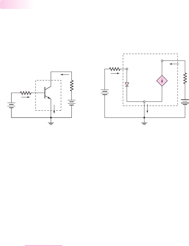
Common-Emitter Circuit
One of the basic transistor circuit configurations is called the common-emitter
circuit. Figure 5.19(a) shows one example of a common-emitter circuit. The emitter
terminal is obviously at ground potential. This circuit configuration will appear in
many amplifiers that will be considered in Chapter 6.
5.2.1
–
–
+
+
V
BB
V
BE
R
B
–
+
V
CC
R
C
–
+
I
B
I
C
I
E
B
E
C
V
CE
–
+
V
BE
(on)
–
+
V
BB
R
B
–
+
V
C
C
R
C
–
+
I
B
I
C
bI
B
I
E
V
CE
B
E
C
(a) (b)
Figure 5.19 (a) Common-emitter circuit with npn transistor and (b) dc equivalent circuit.
Transistor equivalent circuit is shown within the dotted lines with piecewise linear transistor
parameters.
Figure 5.19(a) shows a common-emitter circuit with an npn transistor, and
Figure 5.19(b) shows the dc equivalent circuit. We will assume that the B–E junction
is forward biased, so the voltage drop across that junction is the cut-in or turn-on
voltage
V
BE
(on). When the transistor is biased in the forward-active mode, the col-
lector current is represented as a dependent current source that is a function of the
base current. We are neglecting the reverse-biased junction leakage current and the
Early effect in this case. In the following circuits, we will be considering dc currents
and voltages, so the dc notation for these parameters will be used.
The base current is
I
B
=
V
BB
− V
BE
(on)
R
B
(5.23)
Implicit in Equation (5.23) is that
V
BB
> V
BE
(on), which means that
I
B
> 0
. When
V
BB
< V
BE
(on), the transistor is cut off and
I
B
= 0
.
In the collector–emitter portion of the circuit, we can write
I
C
= β I
B
(5.24)
and
V
CC
= I
C
R
C
+ V
CE
(5.25(a))
or
V
CE
= V
CC
− I
C
R
C
(5.25(b))
In Equation (5.25(b)), we are also implicitly assuming that
V
CE
> V
BE
(on), which
means that the B–C junction is reverse biased and the transistor is biased in the
forward-active mode.
nea80644_ch05_285-368.qxd 06/12/2009 08:42 PM Page 302 F506 Tempwork:Dont' Del Rakesh:June:Rakesh 06-12-09:MHDQ134-05:
Chapter 5 The Bipolar Junction Transistor 303
(a)
+
–
+
–
V
BE
I
B
R
C
= 2 kΩ
R
B
= 220 kΩ
V
CC
= 10 V
V
BB
= 4 V
I
C
V
CE
(b)
+
–
V
BE
= 0.7 V
R
C
= 2 kΩ
V
CC
= 10 V
R
B
= 220 kΩ
V
BB
= 4 V
I
C
= bI
B
= 3 mA
I
E
= I
C
+ I
B
= 3.02 mA
⇒ 15 mA
V
CE
= 10 – (3)(2)
+
–
= 4 V
I
B
=
4 – 0.7
220 kΩ
Figure 5.20 Circuit for Example 5.3: (a) circuit and (b) circuit showing current and voltage
values
Considering Figure 5.19(b), we can see that the power dissipated in the transis-
tor is given by
P
T
= I
B
V
BE
(on) + I
C
V
CE
(5.26(a))
In most cases,
I
C
I
B
and
V
CE
> V
BE
(on) so that a good first approximation of the
power dissipated is given as
P
T
∼
=
I
C
V
CE
(5.26(b))
The principal condition where this approximation is not valid is for a transistor
biased in the saturation mode (discussed later).
EXAMPLE 5.3
Objective: Calculate the base, collector, and emitter currents and the C–E voltage
for a common-emitter circuit. Calculate the transistor power dissipation.
For the circuit shown in Figure 5.19(a), the parameters are:
V
BB
= 4
V,
R
B
=
220 k
,
R
C
= 2
k
,
V
CC
= 10
V,
V
BE
(on) = 0.7
V, and
β = 200
. Figure 5.20(a)
shows the circuit without explicitly showing the voltage sources.
Solution: Referring to Figure 5.20(b), the base current is found as
I
B
=
V
BB
− V
BE
(on)
R
B
=
4 − 0.7
220
⇒ 15 μA
The collector current is
I
C
= β I
B
= (200)(15 μA) ⇒ 3mA
and the emitter current is
I
E
= (1 +β) · I
B
= (201)(15μA) ⇒ 3.02 mA
From Equation (5.25(b)), the collector-emitter voltage is
V
CE
= V
CC
− I
C
R
C
= 10 −(3)(2) = 4V
The power dissipated in the transistor is found to be
P
T
= I
B
V
BE
(on) + I
C
V
CE
= (0.015)(0.7) + (3)(4)
∼
=
I
C
V
CE
nea80644_ch05_285-368.qxd 06/12/2009 08:42 PM Page 303 F506 Tempwork:Dont' Del Rakesh:June:Rakesh 06-12-09:MHDQ134-05:
304 Part 1 Semiconductor Devices and Basic Applications
+
+
–
–
V
BB
V
EB
R
B
+
–
V
CC
R
C
+
–
I
B
I
C
I
E
B
E
C
V
EC
+
–
V
EB
(on)
+
–
V
BB
R
B
+
–
V
C
C
R
C
+
–
I
B
I
C
I
E
V
EC
bI
B
B
E
C
(a) (b)
Figure 5.21 (a) Common-emitter circuit with pnp transistor and (b) dc equivalent circuit.
Transistor equivalent circuit is shown within the dotted lines with piecewise linear transistor
parameters.
or
P
T
∼
=
12 mW
Comment: Since
V
BB
> V
BE
(on) and
V
CE
> V
BE
(on), the transistor is indeed
biased in the forward-active mode. As a note, in an actual circuit, the voltage across
a B–E junction may not be exactly 0.7 V, as we have assumed using the piecewise
linear approximation. This may lead to slight inaccuracies between the calculated
currents and voltages and the measured values. Also note that, if we take the differ-
ence between
I
E
and
I
C
, which is the base current, we obtain
I
B
= 20 μ
A rather than
15
μ
A. The difference is the result of roundoff error in the emitter current.
EXERCISE PROBLEM
Ex 5.3: The circuit elements in Figure 5.20(a) are changed to
V
CC
= 3.3
V,
V
BB
= 2
V,
R
C
= 3.2
k
, and
R
B
= 430
k
. The transistor parameters are
β = 150
and
V
BE
= 0.7
V. Calculate
I
B
,
I
C
,
V
CE
, and the power dissipated in the
transistor. (Ans.
I
B
= 3.02 μ
A,
I
C
= 0.453
mA,
V
CE
= 1.85
V,
P = 0.838
mW)
Figure 5.21(a) shows a common-emitter circuit with a pnp bipolar transistor, and
Figure 5.21(b) shows the dc equivalent circuit. In this circuit, the emitter is at ground
potential, which means that the polarities of the
V
BB
and
V
CC
power supplies must
be reversed compared to those in the npn circuit. The analysis proceeds exactly as
before, and we can write
I
B
=
V
BB
− V
EB
(on)
R
B
(5.27)
I
C
= β I
B
(5.28)
and
V
EC
= V
CC
− I
C
R
C
(5.29)
We can see that Equations (5.27), (5.28), and (5.29) for the pnp bipolar transis-
tor in the common-emitter configuration are exactly the same as Equations (5.23),
(5.24), and (5.25(b)) for the npn bipolar transistor in a similar circuit, if we properly
define the current directions and voltage polarities.
nea80644_ch05_285-368.qxd 06/12/2009 08:42 PM Page 304 F506 Tempwork:Dont' Del Rakesh:June:Rakesh 06-12-09:MHDQ134-05:
Chapter 5 The Bipolar Junction Transistor 305
In many cases, the pnp bipolar transistor will be reconfigured in a circuit so that
positive voltage sources, rather than negative ones, can be used. We see this in the
following example.
EXAMPLE 5.4
Objective: Analyze the common-emitter circuit with a pnp transistor.
For the circuit shown in Figure 5.22(a), the parameters are:
V
BB
= 1.5
V,
R
B
= 580
k
,
V
+
= 5
V,
V
EB
(on) = 0.6
V, and
β = 100
. Find
I
B
,
I
C
,
I
E
, and
R
C
such that
V
EC
=
1
2
V
+
.
(a)
+
–
+
–
I
B
R
C
R
B
= 580 kΩ
V
+
= 5 V
V
BB
= 1.5 V
I
E
I
C
V
EB
V
EC
+
–
+
–
0.6 V
R
C
R
B
= 580 kΩ
V
+
= 5 V
V
BB
= +1.5 V
I
E
= I
C
+ I
B
= 0.505 mA
I
C
= b I
B
= 0.5 mA
=
⇒ 5 mA
V
EC
= 2.5 V
I
B
=
(5 – 0.6) – 1.5
580 kΩ
5 – 2.5
R
C
(b)
Figure 5.22 Circuit for Example 5.4; (a) circuit and (b) circuit showing current and voltage
values
Solution:
Writing a Kirchhoff voltage law equation around the E–B loop, we find the
base current to be
I
B
=
V
+
− V
EB
(on) − V
BB
R
B
=
5 − 0.6 −1.5
580
⇒ 5μA
The collector current is
I
C
= β I
B
= (100)(5μA) ⇒ 0.5mA
and the emitter current is
I
E
= (1 +β)I
B
= (101)(5μA) ⇒ 0.505 mA
For a C–E voltage of
V
EC
=
1
2
V
+
= 2.5
V,
R
C
is
R
C
=
V
+
− V
EC
I
C
=
5 − 2.5
0.5
= 5k
Comment: In this case, the difference between
V
+
and
V
BB
is greater than the tran-
sistor turn-on voltage, or
(V
+
− V
BB
)>V
EB
(on)
. Also, because
V
EC
> V
EB
(on),
the pnp bipolar transistor is biased in the forward-active mode.
Discussion: In this example, we used an emitter-base turn-on voltage of
V
EB
(on) = 0.6
V, whereas previously we used a value of 0.7 V. We must keep in
mind that the turn-on voltage is an approximation and the actual base–emitter volt-
age will depend on the type of transistor used and the current level. In most situa-
tions, choosing a value of 0.6 V or 0.7 V will make only minor differences. However,
most people tend to use the value of 0.7 V.
nea80644_ch05_285-368.qxd 06/12/2009 08:42 PM Page 305 F506 Tempwork:Dont' Del Rakesh:June:Rakesh 06-12-09:MHDQ134-05:
306 Part 1 Semiconductor Devices and Basic Applications
(a)
i
C
(mA)
I
BQ
= 15 mA
25
30
10
0246810
0
1
2
3
4
5
6
v
CE
(V)
V
CE
(sat)
I
C
(sat)
i
B
= 5
Forward-active mode
20
Saturation
Load line
Q-point
Cutoff
i
B
(mA)
V
BB
= 4 V
v
BE
V
BE
(on) = 0.7 V
0
B–E junction
characteristics
Load line
Quiescent base
current and
B–E voltage
I
BQ
= 15
= 18.2
V
BB
R
B
(b)
Figure 5.23 (a) Base–emitter junction piecewise linear i–
v
characteristics and the input load
line, and (b) common-emitter transistor characteristics and the collector–emitter load line
showing the Q-point for the circuit shown in Example 5.3 (Figure 5.20)
EXERCISE PROBLEM
Ex 5.4: The circuit elements in Figure 5.22(a) are
V
+
= 3.3
V,
V
BB
= 1.2
V,
R
B
= 400
k
, and
R
C
= 5.25
k
. The transistor parameters are
β = 80
and
V
EB
(
on
)
= 0.7
V. Determine
I
B
,
I
C
, and
V
EC
. (Ans.
I
B
= 3.5 μ
A,
I
C
= 0.28
mA,
V
EC
= 1.83
V)
The dc equivalent circuits, such as those given in Figures 5.19(b) and 5.21(b),
are useful initially in analyzing transistor circuits. From this point on, however, we
will not explicitly draw the equivalent circuit. We will simply analyze the circuit
using the transistor circuit symbols, as in Figures 5.20 and 5.22.
COMPUTER ANALYSIS EXERCISE
PS 5.1: (a) Verify the results of Example 5.3 with a PSpice analysis. Use a stan-
dard transistor. (b) Repeat the analysis for
R
B
= 180
k
. (c) Repeat the analysis
for
R
B
= 260
k
. What can be said about
R
B
limiting the base current?
Load Line and Modes of Operation
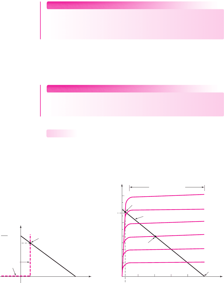
The load line can help us visualize the characteristics of a transistor circuit. For the
common-emitter circuit in Figure 5.20(a), we can use a graphical technique for both
the B–E and C–E portions of the circuit. Figure 5.23(a) shows the piecewise linear
characteristics for the B–E junction and the input load line. The input load line is
5.2.2
nea80644_ch05_285-368.qxd 06/12/2009 08:42 PM Page 306 F506 Tempwork:Dont' Del Rakesh:June:Rakesh 06-12-09:MHDQ134-05:

Chapter 5 The Bipolar Junction Transistor 307
obtained from Kirchhoff’s voltage law equation around the B–E loop, written as
follows:
I
B
=
V
BB
R
B
−
V
BE
R
B
(5.30)
Both the load line and the quiescent base current change as either or both
V
BB
and
R
B
change. The load line in Figure 5.23(a) is essentially the same as the load line
characteristics for diode circuits, as shown in Chapter 1.
For the C–E portion of the circuit in Figure 5.20(a), the load line is found by
writing Kirchhoff’s voltage law equation around the C–E loop. We obtain
V
CE
= V
CC
− I
C
R
C
(5.31(a))
which can be written in the form
I
C
=
V
CC
R
C
−
V
CE
R
C
= 5 −
V
CE
2
(mA)
(5.31(b))
Equation (5.31(b)) is the load line equation, showing a linear relationship between
the collector current and collector–emitter voltage. Since we are considering the dc
analysis of the transistor circuit, this relationship represents the dc load line. The ac
load line is presented in the next chapter.
Figure 5.23(b) shows the transistor characteristics for the transistor in Exam-
ple 5.3, with the load line superimposed on the transistor characteristics. The two end
points of the load line are found by setting
I
C
= 0
, yielding
V
CE
= V
CC
= 10
V, and
by setting
V
CE
= 0
, yielding
I
C
= V
CC
/R
C
= 5
mA.
The quiescent point, or Q-point, of the transistor is given by the dc collector cur-
rent and the collector–emitter voltage. The Q-point is the intersection of the load line
and the
I
C
versus
V
CE
curve corresponding to the appropriate base current. The
Q-point also represents the simultaneous solution to two expressions. The load line is
useful in visualizing the bias point of the transistor. In the figure, the Q-point shown
is for the transistor in Example 5.3.
As previously stated, if the power supply voltage in the base circuit is smaller
than the turn-on voltage, then
V
BB
< V
BE
(on) and
I
B
= I
C
= 0
, and the transistor is
in the cutoff mode. In this mode, all transistor currents are zero, neglecting leakage
currents, and for the circuit shown in Figure 5.20(a),
V
CE
= V
CC
= 10
V.
As
V
BB
increases
(V
BB
> V
BE
(on))
, the base current
I
B
increases and the Q-
point moves up the load line. As
I
B
continues to increase, a point is reached where
the collector current
I
C
can no longer increase. At this point, the transistor is biased
in the saturation mode; that is, the transistor is said to be in saturation. The B–C
junction becomes forward biased, and the relationship between the collector and
base currents is no longer linear. The transistor C–E voltage in saturation,
V
CE
(sat),
is less than the B–E cut-in voltage. The forward-biased B–C voltage is always less
than the forward-biased B–E voltage, so the C–E voltage in saturation is a small pos-
itive value. Typically,
V
CE
(sat) is in the range of 0.1 to 0.3 V.
EXAMPLE 5.5
Objective: Calculate the currents and voltages in a circuit when the transistor is dri-
ven into saturation.
For the circuit shown in Figure 5.24, the transistor parameters are:
β = 100
, and
V
BE
(on) = 0.7
V. If the transistor is biased in saturation, assume
V
CE
(sat) = 0.2
V.
nea80644_ch05_285-368.qxd 06/12/2009 08:42 PM Page 307 F506 Tempwork:Dont' Del Rakesh:June:Rakesh 06-12-09:MHDQ134-05: