Neamen D. Microelectronics: Circuit Analysis and Design
Подождите немного. Документ загружается.

248 Part 1 Semiconductor Devices and Basic Applications
EXAMPLE 4.13
Objective: Determine the small-signal voltage gain of the CMOS amplifier.
For the circuit shown in Figure 4.45(a), assume transistor parameters of
V
TN
=+0.8
V,
V
TP
=−0.8
V,
k
n
= 80 μA/V
2
,
k
p
= 40 μA/V
2
,
(W/L)
n
= 15
,
(W/L)
p
= 30
, and
λ
n
= λ
p
= 0.01 V
−1
. Also, assume
I
Bias
= 0.2
mA.
Solution: The transconductance of the NMOS driver is
g
mn
= 2
K
n
I
DQ
= 2
k
n
2
W
L
n
I
Bias
= 2
0.08
2
(15)(0.2) = 0.693 mA/V
Since
λ
n
= λ
p
, the output resistances are
r
on
= r
op
=
1
λI
DQ
=
1
(0.01)(0.2)
= 500 k
and M
2
are shown. Point A is the transition point for M
1
and point B is the transition
point for M
2
. The Q-point, to establish an amplifier, should be approximately
halfway between points A and B, so that both transistors are biased in their saturation
regions. The voltage transfer characteristics are shown in Figure 4.45(d). Shown on
the curve are the same transition points A and B and the desired Q-point.
We again apply the small-signal equivalent circuits to find the small-signal volt-
age gain. With v
SG2
held constant, the equivalent resistance looking into the drain of
M
2
is just
R
o
= r
op
. The small-signal equivalent circuit of the inverter is then as given
in Figure 4.46. The subscripts n and p refer to the n-channel and p-channel transis-
tors, respectively. We may note that the body terminal of M
1
will be tied to ground,
which is the same as the source of M
1
, and the body terminal of M
2
will be tied to
V
DD
, which is the same as the source of M
2
. Hence, there is no body effect in this
circuit.
The small-signal voltage gain is
A
v
=
V
o
V
i
=−g
mn
(r
on
r
op
)
(4.52)
Again for this circuit, the small-signal voltage gain is directly proportional to the
output resistances of the two transistors.
+
–
V
i
+
–
V
gs
g
mn
V
gs
r
on
r
op
V
o
M
1
M
2
Figure 4.46 Small-signal equivalent circuit of the CMOS common-source amplifier
nea80644_ch04_205-284.qxd 06/12/2009 08:00 PM Page 248 F506 Tempwork:Dont' Del Rakesh:June:Rakesh 06-12-09:MHDQ134-04:

Chapter 4 Basic FET Amplifiers 249
The small-signal voltage gain is then
A
v
=−g
m
(r
on
r
op
) =−(0.693)(500500) =−173
Comment: The voltage gain of the CMOS amplifier is on the same order of magni-
tude as the NMOS amplifier with depletion load. However, the CMOS amplifier does
not suffer from the body effect.
Discussion: In the circuit configuration shown in Figure 4.45(a), we must again
apply a dc voltage to the gate of M
1
to achieve the “proper” Q-point. We will show in
later chapters using more sophisticated circuits how the Q-point is more easily
established with current-source biasing. However, this circuit demonstrates the basic
principles of the CMOS common-source amplifier.
EXERCISE PROBLEM
Ex 4.13: For the circuit shown in Figure 4.45(a), assume transistor para-
meters of
V
TN
=+0.5
V,
V
TP
=−0.5
V,
k
n
= 80 μA/V
2
,
k
p
= 40 μA/V
2
, and
λ
n
= λ
p
= 0.015 V
−1
. Assume
I
Bias
= 0.1
mA. Assume M
2
and M
3
are matched.
Find the width-to-length ratio of M
1
such that the small-signal voltage gain is
A
v
=−250
. (Ans.
(W/L)
1
= 35.2
)
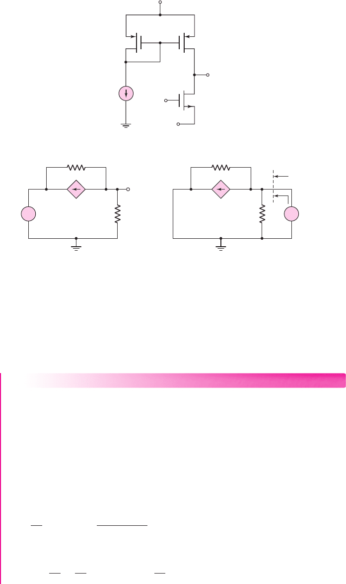
CMOS Source-Follower Amplifier
The same basic CMOS circuit configuration can be used to form a CMOS source-
follower amplifier. Figure 4.47(a) shows a source-follower circuit. We see that for
this source-follower circuit, the active load, which is M
2
, is an n-channel rather than
a p-channel device. The input signal is applied to the gate of M
1
and the output is at
the source of M
1
.
The small-signal equivalent circuit of this source-follower is shown in
Figure 4.47(b). This circuit, with two signal grounds, is redrawn as shown in
Figure 4.47(c) to combine the signal grounds.
EXAMPLE 4.14
Objective: Determine the small-signal voltage gain and output resistance of the
source-follower amplifier shown in Figure 4.47(a).
Assume the reference bias current is
I
Bias
= 0.20
mA and the bias voltage is
V
DD
= 3.3
V. Assume that all transistors are matched (identical) with parameters
V
TN
= 0.4
V,
K
n
= 0.20
mA/V
2
, and
λ = 0.01 V
−1
.
We may note that since M
3
and M
2
are matched transistors and have the same
gate-to-source voltages, the drain current in M
1
is
I
D1
= I
Bias
= 0.2
mA.
Solution (voltage gain): From Figure 4.47(c), we find the small-signal output volt-
age to be
V
o
= g
m1
V
gs
(r
o1
r
o2
)
A KVL equation around the outside loop produces
V
i
= V
gs
+ V
o
= V
gs
+ g
m1
V
gs
(r
o1
r
o2
)
nea80644_ch04_205-284.qxd 06/13/2009 01:58 PM Page 249 F506 Hard disk:Desktop Folder:ALI-06-13-09:MHDQ134-04 Folder:MHDQ134-0
250 Part 1 Semiconductor Devices and Basic Applications
or
V
gs
=
V
i
1 + g
m1
(r
o1
r
o2
)
Substituting this equation for V
gs
into the output voltage expression, we obtain the
small-signal voltage gain as
A
v
=
V
o
V
i
=
g
m1
(r
o1
r
o2
)
1 + g
m1
(r
o1
r
o2
)
The small-signal equivalent circuit parameters are determined to be
g
m1
= 2
K
n
I
D1
= 2
(0.20)(0.20) = 0.40 mA/V
and
r
o1
= r
o2
=
1
λI
D
=
1
(0.01)(0.20)
= 500 k
The small-signal voltage gain is then
A
v
=
(0.40)(500500)
1 + (0.40)(500500)
V
DD
v
I
V
i
r
o2
r
o1
r
o2
V
o
V
o
r
o1
V
gs
g
m
V
gs
g
m
V
gs
I
Bias
M
3
M
2
M
1
Driver
Load
v
O
(a)
(c)
(b)
+
–
+
–
V
gs
V
i
+–
+
–
+
–
r
o1
r
o2
R
o
g
m
V
gs
(d)
V
gs
V
x
+–
+
–
I
x
Figure 4.47 (a) All NMOS source-follower circuit, (b) small-signal equivalent circuit,
(c) reconfiguration of small-signal equivalent circuit, and (d) small-signal equivalent
circuit for determining the output resistance
nea80644_ch04_205-284.qxd 06/12/2009 08:00 PM Page 250 F506 Tempwork:Dont' Del Rakesh:June:Rakesh 06-12-09:MHDQ134-04:

Chapter 4 Basic FET Amplifiers 251
or
A
v
= 0.990
Solution (output resistance): The output resistance can be determined from the
equivalent circuit shown in Figure 4.47(d). The independent source V
i
is set equal to
zero and a test voltage V
x
is applied to the output.
Summing currents at the output node, we find
I
x
+ g
m1
V
gs
=
V
x
r
o2
+
V
x
r
o1
From the circuit, we see that
V
gs
=−V
x
. We then have
I
x
= V
x
g
m1
+
1
r
o2
+
1
r
o1
The output resistance is then given as
R
o
=
V
x
I
x
=
1
g
m1
r
o2
r
o1
We find
R
o
=
1
0.40
500
500
or
R
o
= 2.48 k
Comment: A voltage gain of
A
v
= 0.99
is typical of a source-follower circuit. An
output resistance of
R
o
= 2.48
k is relatively small for a MOSFET circuit and is
also a characteristic of a source-follower circuit.
EXERCISE PROBLEM
Ex 4.14: The transconductance g
m
of the transistor in the circuit of Figure 4.47
is to be changed by changing the bias current such that the output resistance of
the circuit is
R
o
= 2
k. Assume all other parameters are as given in Exam-
ple 4.14. (a) What are the required values of g
m
and I
Bias
? (b) Using the results
of part (a), what is the small-signal voltage gain? (Ans. (a)
I
D
= 0.3125
mA;
(b)
A
v
= 0.988
)
COMPUTER ANALYSIS EXERCISE
PS 4.1: Using a PSpice analysis, investigate the small-signal voltage gain and
output resistance of the source-follower circuit shown in Figure 4.47 taking into
account the body effect.
CMOS Common-Gate Amplifier
Figure 4.48(a) shows a common-gate circuit. We see that in this common-gate
circuit, the active load is the PMOS device M
2
. The input signal is applied to the
source of M
1
and the output is at the drain of M
1
.
nea80644_ch04_205-284.qxd 06/12/2009 08:00 PM Page 251 F506 Tempwork:Dont' Del Rakesh:June:Rakesh 06-12-09:MHDQ134-04:
252 Part 1 Semiconductor Devices and Basic Applications
The small-signal equivalent circuit of the common-gate circuit is shown in
Figure 4.48(b).
EXAMPLE 4.15
Objective: Determine the small-signal voltage gain and output resistance of the
common-gate circuit shown in Figure 4.48(a).
Assume the reference bias current is
I
Bias
= 0.20
mA and the bias voltage is
V
DD
= 3.3
V. Assume that the transistor parameters are
V
TN
=+0.4
V,
V
TP
=
−0.4V
,
K
n
= 0.20
mA/V
2
,
K
p
= 0.20
mA/V
2
, and
λ
n
= λ
p
= 0.01 V
−1
.
We may note that, since M
2
and M
3
are matched transistors and have the same
source-to-gate voltage, the bias current in M
1
is
I
D1
= I
Bias
= 0.20
mA.
Solution (voltage gain): From Figure 4.48(b), we can sum currents at the output
node and obtain
V
o
r
o2
+ g
m1
V
gs
+
V
o
−(−V
gs
)
r
o1
= 0
or
V
o
1
r
o2
+
1
r
o1
+ V
gs
g
m1
+
1
r
o1
= 0
+
–
r
o2
r
o1
V
o
G
DS
g
m
V
gs
(b)
V
gs
V
i
+
–
r
o2
r
o1
g
m
V
gs
= 0
(c)
V
gs
= 0
V
x
+
–
+
–
R
o
I
x
V
DD
v
I
I
Bias
V
Bias
M
3
M
1
M
2
Load
Driver
v
O
(a)
Figure 4.48 (a) CMOS common-gate amplifier, (b) small-signal equivalent circuit, and
(c) small-signal equivalent circuit for determining the output resistance
nea80644_ch04_205-284.qxd 06/12/2009 08:00 PM Page 252 F506 Tempwork:Dont' Del Rakesh:June:Rakesh 06-12-09:MHDQ134-04:

Chapter 4 Basic FET Amplifiers 253
From the circuit, we see that
V
gs
=−V
i
. We then find the small-signal voltage gain
to be
A
v
=
g
m1
+
1
r
o1
1
r
o2
+
1
r
o1
We find the small-signal equivalent circuit parameters to be
g
m1
= 2
K
n
I
D1
= 2
(0.20)(0.20) = 0.40 mA/V
and
r
o1
= r
o2
=
1
λI
D1
=
1
(0.01)(0.20)
= 500 k
We then find
A
v
=
0.40 +
1
500
1
500
+
1
500
or
A
v
= 101
Solution (output resistance): The output resistance can be found from Figure 4.48(c).
Summing currents at the output node, we find
I
x
=
V
x
r
o2
+ g
m1
V
gs
+
V
x
−(−V
gs
)
r
o1
However,
V
gs
= 0
so that
g
m1
V
gs
= 0
. We then find
R
o
=
V
x
I
x
= r
o1
r
o2
= 500500
or
R
o
= 250 k
Comment: A voltage gain of
A
v
=+101
is typical of a common-gate amplifier. The
output signal is in phase with respect to the input signal and the gain is relatively
large. Also, a large output resistance of
R
o
= 250
k is typical of a common-gate
amplifier in that the circuit acts like a current source.
EXERCISE PROBLEM
Ex 4.15: The transconductance g
m
of the transistor in the circuit of Figure 4.48 is
to be changed by changing the bias current such that the small-signal voltage gain
is
A
v
= 120
. Assume all other parameters are as given in Example 4.15. (a) What
are the required values of g
m
and I
Bias
? (b) Using the results of part (a), what is the
output resistance? (Ans. (a)
I
D
= 0.14
mA,
g
m
= 0.335
mA/V; (b)
R
o
= 357 k
)
nea80644_ch04_205-284.qxd 06/12/2009 08:00 PM Page 253 F506 Tempwork:Dont' Del Rakesh:June:Rakesh 06-12-09:MHDQ134-04:
254 Part 1 Semiconductor Devices and Basic Applications
COMPUTER ANALYSIS EXERCISE
PS 4.2: Using a PSpice analysis, investigate the small-signal voltage gain and
output resistance of the common-gate amplifier shown in Figure 4.48 taking into
account the body effect.
Test Your Understanding
TYU 4.11 For the enhancement load amplifier shown in Figure 4.39(a), the parame-
ters are:
V
TND
= V
TNL
= 0.8
V,
k
n
= 40 μA/V
2
,
(W/L)
D
= 80,(W/L)
L
= 1
, and
V
DD
= 5
V. Determine the small-signal voltage gain. Determine V
GS
such that the
Q-point is in the middle of the saturation region. (Ans.
A
v
=−8.94
,
V
GS
= 1.01
V)
4.8 MULTISTAGE AMPLIFIERS
Objective: • Analyze multitransistor or multistage amplifiers and
understand the advantages of these circuits over single-transistor
amplifiers.
In most applications, a single-transistor amplifier will not be able to meet the
combined specifications of a given amplification factor, input resistance, and output
resistance. For example, the required voltage gain may exceed that which can be
obtained in a single-transistor circuit. We will consider, here, the ac analysis of the
two multitransistor circuits investigated in Chapter 3.
Multistage Amplifier: Cascade Circuit
The circuit shown in Figure 4.49 is a cascade of a common-source amplifier followed by
a source-follower amplifier. As shown previously, the common-source amplifier
4.8.1
v
i
R
1
=
383 kΩ
C
C
C
S
R
D1
=
16.1 kΩ
R
S1
=
3.9 kΩ
R
S2
=
8 kΩ
M
1
v
o
R
L
=
4 kΩ
C
C2
V
+
= 5 V
V
–
= –5 V
M
2
R
i
R
Si
=
4 kΩ
R
o
+
–
R
2
=
135 kΩ
Figure 4.49 Common-source amplifier in cascade with source follower
nea80644_ch04_205-284.qxd 06/12/2009 08:00 PM Page 254 F506 Tempwork:Dont' Del Rakesh:June:Rakesh 06-12-09:MHDQ134-04:
Chapter 4 Basic FET Amplifiers 255
provides a small-signal voltage gain and the source follower has a low output impedance
and provides the required output current. The resistor values are those determined in
Section 3.5.1 of the previous chapter.
The midband small-signal voltage gain of the multistage amplifier is determined
by assuming that all external coupling capacitors act as short circuits and inserting
the small-signal equivalent circuits for the transistors.
EXAMPLE 4.16
Objective: Determine the small-signal voltage gain of a multistage cascade circuit.
Consider the circuit shown in Figure 4.49. The transistor parameters are
K
n1
= 0.5
mA/V
2
,
K
n2
= 0.2
mA/V
2
,
V
TN1
= V
TN2
= 1.2
V, and
λ
1
= λ
2
= 0
. The
quiescent drain currents are
I
D1
= 0.2
mA and
I
D2
= 0.5
mA.
Solution: The small-signal equivalent circuit is shown in Figure 4.50. The small-
signal transconductance parameters are
g
m1
= 2
K
n1
I
D1
= 2
(0.5)(0.2) = 0.632 mA/V
and
g
m2
= 2
K
n2
I
D2
= 2
(0.2)(0.5) = 0.632 mA/V
The output voltage is
V
o
= g
m2
V
gs2
(R
S2
R
L
)
Also,
V
gs2
+ V
o
=−g
m1
V
gs1
R
D1
where
V
gs1
=
R
i
R
i
+ R
Si
· V
i
Then
V
gs2
=−g
m1
R
D1
R
i
R
i
+ R
Si
· V
i
− V
o
Therefore
V
o
= g
m2
−g
m1
R
D1
R
i
R
i
+ R
Si
· V
i
− V
o
(R
S2
R
L
)
V
o
g
m1
V
gs1
V
gs2
–
+
V
gs1
–
+
g
m2
V
gs2
V
i
R
i
R
Si
R
1
⎪⎪ R
2
R
D1
R
L
R
S2
+
–
Figure 4.50 Small-signal equivalent circuit of NMOS cascade circuit
nea80644_ch04_205-284.qxd 06/12/2009 08:00 PM Page 255 F506 Tempwork:Dont' Del Rakesh:June:Rakesh 06-12-09:MHDQ134-04:

256 Part 1 Semiconductor Devices and Basic Applications
The small-signal voltage gain is then
A
v
=
V
o
V
i
=
−g
m1
g
m2
R
D1
(R
S2
R
L
)
1 + g
m2
(R
S2
R
L
)
·
R
i
R
i
+ R
Si
or
A
v
=
−(0.632)(0.632)(16.1)(84)
1 + (0.632)(84)
·
100
100 + 4
=−6.14
Comment: Since the small-signal voltage gain of the source follower is slightly
less than 1, the overall gain is due essentially to the common-source input stage.
Also, as shown previously, the output resistance of the source follower is small,
which is desirable in many applications.
EXERCISE PROBLEM
Ex 4.16: For the cascade circuit shown in Figure 4.49, the transistor and circuit
parameters are given in Example 4.16. Calculate the small-signal output resis-
tance R
o
. (The small-signal equivalent circuit is shown in Figure 4.50.) (Ans.
R
o
= 1.32 k
)
Multistage Amplifier: Cascode Circuit
Figure 4.51 shows a cascode circuit with n-channel MOSFETs. Transistor M
1
is
connected in a common-source configuration and M
2
is connected in a common-gate
configuration. The advantage of this type of circuit is a higher frequency response,
which will be discussed in Chapter 7. The resistor values are those determined in
Section 3.5.2 of the previous chapter.
We will consider additional multistage and multitransistor circuits in Chapters 11
and 13.
4.8.2
R
3
=
54.6 kΩ
v
i
C
C
R
2
=
150 kΩ
R
1
=
95.4 kΩ
C
G
C
S
R
D
= 2.5 kΩ
V
+
= 5 V
V
–
= –5 V
v
O
R
S
=
10 kΩ
M
1
M
2
+
–
Figure 4.51 NMOS cascode circuit
nea80644_ch04_205-284.qxd 06/12/2009 08:00 PM Page 256 F506 Tempwork:Dont' Del Rakesh:June:Rakesh 06-12-09:MHDQ134-04:
Chapter 4 Basic FET Amplifiers 257
V
o
g
m1
V
gs1
V
gs1
–
+
g
m2
V
gs2
= g
m1
V
gs1
V
i
R
D
R
3
⎪⎪ R
2
+
–
Figure 4.52 Small-signal equivalent circuit of NMOS cascode circuit
Since
V
gs1
= V
i
, the small-signal voltage gain is
A
v
=
V
o
V
i
=−g
m1
R
D
or
A
v
=−(1.13)(2.5) =−2.83
Comment: The small-signal voltage gain is essentially the same as that of a single
common-source amplifier stage. The addition of a common-gate transistor will
increase the frequency bandwidth, as we will see in a later chapter.
EXERCISE PROBLEM
Ex 4.17: The transistor parameters of the NMOS cascode circuit in Figure 4.51
are
V
TN1
= V
TN2
= 0.8
V,
K
n1
= K
n2
= 3
mA/V
2
, and
λ
1
= λ
2
= 0
. (a) Deter-
mine
I
DQ
,
V
DSQ1
, and
V
DSQ2
. (b) Determine the small-signal voltage gain. (Ans.
(a)
I
DQ
= 0.471
mA,
V
DSQ1
= 2.5
V,
V
DSQ2
= 1.61
V; (b)
A
v
=−5.94)
EXAMPLE 4.17
Objective: Determine the small-signal voltage gain of a cascode circuit.
Consider the cascode circuit shown in Figure 4.51. The transistor parameters are
K
n1
= K
n2
= 0.8
mA/V
2
,
V
TN1
= V
TN2
= 1.2
V, and
λ
1
= λ
2
= 0
. The quiescent
drain current is
I
D
= 0.4
mA in each transistor. The input signal to the circuit is
assumed to be an ideal voltage source.
Solution: Since the transistors are identical and since the current in the two transis-
tors is the same, the small-signal transconductance parameters are
g
m1
= g
m2
= 2
K
n
I
D
= 2
(0.8)(0.4) = 1.13 mA/V
The small-signal equivalent circuit is shown in Figure 4.52. Transistor M
1
supplies
the source current of M
2
with the signal current (g
m1
V
i
). Transistor M
2
acts as a
current follower and passes this current on to its drain terminal. The output voltage is
therefore
V
o
=−g
m1
V
gs1
R
D
nea80644_ch04_205-284.qxd 06/12/2009 08:00 PM Page 257 F506 Tempwork:Dont' Del Rakesh:June:Rakesh 06-12-09:MHDQ134-04: