Neamen D. Microelectronics: Circuit Analysis and Design
Подождите немного. Документ загружается.


268 Part 1 Semiconductor Devices and Basic Applications
PROBLEMS
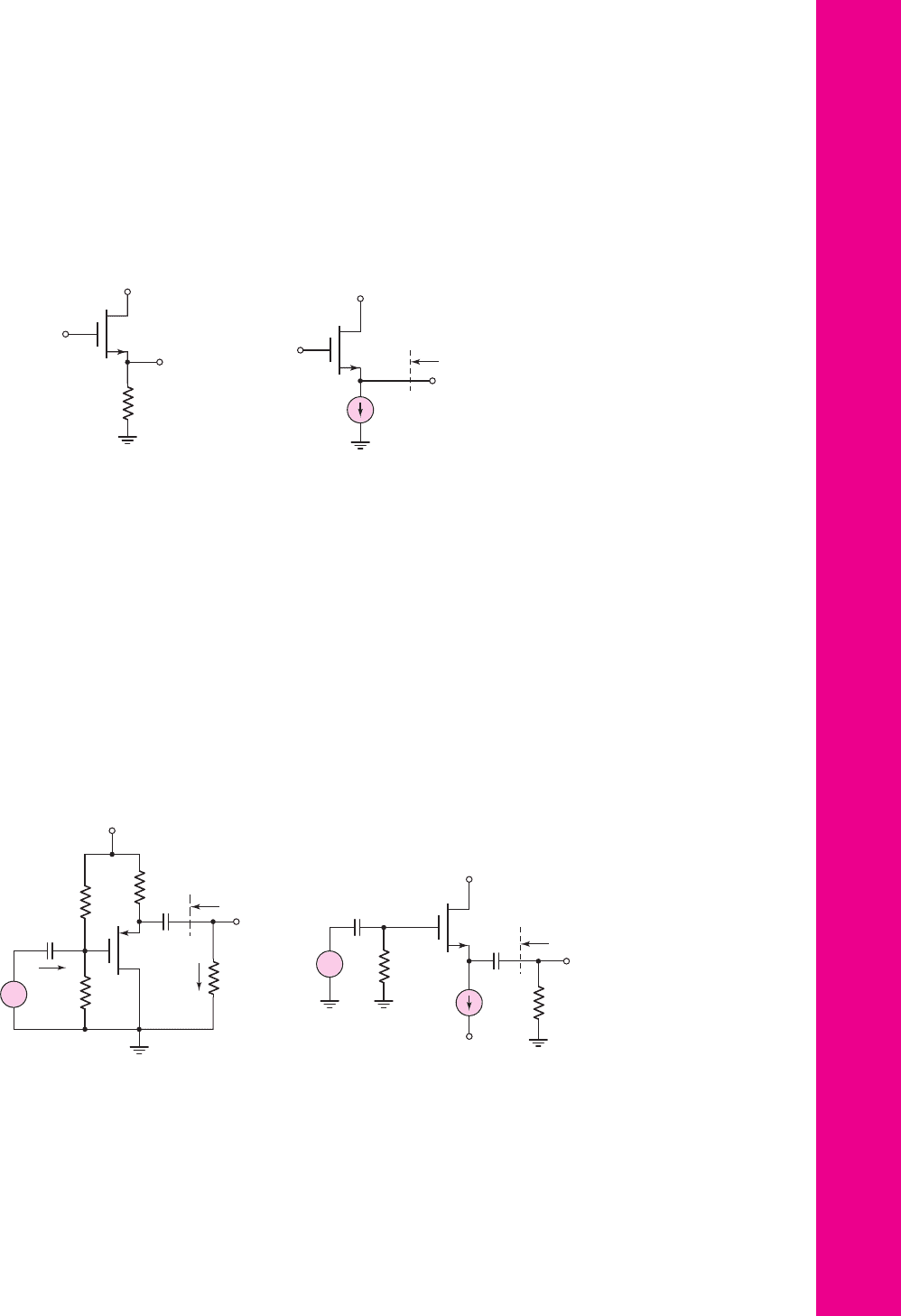
Section 4.1 The MOSFET Amplifier
4.1 An NMOS transistor has parameters
V
TN
= 0.4
V,
k
n
= 100 μ
A/V
2
, and
λ = 0.02
V
−1
. (a) (i) Determine the width-to-length ratio
W/L
such that
g
m
= 0.5
mA/V at
I
DQ
= 0.5
mA when biased in the saturation region.
(ii) Calculate the required value of
V
GSQ
. (b) Repeat part (a) for
I
DQ
= 0.15
mA.
4.2 A PMOS transistor has parameters
V
TP
=−0.6
V,
k
p
= 40 μ
A/V
2
, and
λ = 0.015
V
−1
. (a) (i) Determine the width-to-length ratio
(W/L)
such that
g
m
= 1.2
mA/V at
I
DQ
= 0.15
mA. (ii) What is the required value of
V
SGQ
? (b) Repeat part (a) for
I
DQ
= 0.50
mA.
4.3 An NMOS transistor is biased in the saturation region at a constant
V
GS
.
The drain current is
I
D
= 3
mA at
V
DS
= 5
V and
I
D
= 3.4
mA at
V
DS
=
10 V. Determine
λ
and r
o
.
4.4 The minimum value of small-signal resistance of a PMOS transistor is to
be
r
o
= 100
k. If
λ = 0.012 V
−1
, calculate the maximum allowed value
of I
D
.
4.5 An n-channel MOSFET is biased in the saturation region at a constant
V
GS
.
(a) The drain current is
I
D
= 0.250
mA at
V
DS
= 1.5
V and
I
D
= 0.258
mA
at
V
DS
= 3.3
V. Determine the value of
λ
and
r
o
. (b) Using the results of
part (a), determine
I
D
at
V
DS
= 5
V.
4.6 The value of
λ
for a MOSFET is
0.02 V
−1
. (a) What is the value of r
o
at
(i)
I
D
= 50 μA
and at (ii)
I
D
= 500 μA
? (b) If
V
DS
increases by 1 V, what
is the percentage increase in I
D
for the conditions given in part (a)?
4.7 A MOSFET with
λ = 0.01 V
−1
is biased in the saturation region at
I
D
=
0.5 mA. If
V
GS
and
V
DS
remain constant, what are the new values of I
D
and
r
o
if the channel length L is doubled?
4.8 The parameters of the circuit in Figure 4.1 are
V
DD
= 3.3
V and
R
D
= 5
k
. The transistor parameters are
k
n
= 100 μ
A/V
2
,
W/L = 40
,
V
TN
= 0.4 V, and λ = 0.025
V
−1
. (a) Find
I
DQ
and
V
GSQ
such that
V
DSQ
= 1.5
V. (b) Determine the small-signal voltage gain.
4.9 The circuit shown in Figure 4.1 has parameters
V
DD
= 2.5
V and
R
D
= 10
k
. The transistor is biased at
I
DQ
= 0.12
mA. The transistor pa-
rameters are
V
TN
= 0.3
V,
k
n
= 100 μ
A/V
2
, and
λ = 0
. (a) Design the
W/L
ratio of the transistor such that the small-signal voltage gain is
A
v
=−3.8
. (b) Repeat part (a) for
A
v
=−5.0
.
4.10 For the circuit shown in Figure 4.1, the transistor parameters are
V
TN
= 0.6
V,
k
n
= 80 μ
A/V
2
, and
λ = 0.015
V
−1
. Let
V
DD
= 5
V. (a) De-
sign the transistor width-to-length ratio
W/L
and the resistance
R
D
such that
I
DQ
= 0.5
mA,
V
GSQ
= 1.2
V, and
V
DSQ
= 3
V. (b) Determine
g
m
and
r
o
.
(c) Determine the small-signal voltage gain
A
v
= v
o
/v
i
.
*4.11 In our analyses, we assumed the small-signal condition given by Equa-
tion (4.4). Now consider Equation (4.3(b)) and let
v
gs
= V
gs
sin ωt
. Show
that the ratio of the signal at frequency
2ω
to the signal at frequency
ω
is
given by
V
gs
/[4(V
GS
− V
TN
)]
. This ratio, expressed in a percentage, is
called the second-harmonic distortion. [Hint: Use the trigonometric iden-
tity
sin
2
θ =
1
2
−
1
2
cos 2θ
.]
4.12 Using the results of Problem 4.11, find the peak amplitude V
gs
that produces
a second-harmonic distortion of 1 percent if
V
GS
= 3
V and
V
TN
= 1
V.
nea80644_ch04_205-284.qxd 06/12/2009 08:00 PM Page 268 F506 Tempwork:Dont' Del Rakesh:June:Rakesh 06-12-09:MHDQ134-04:
Chapter 4 Basic FET Amplifiers 269
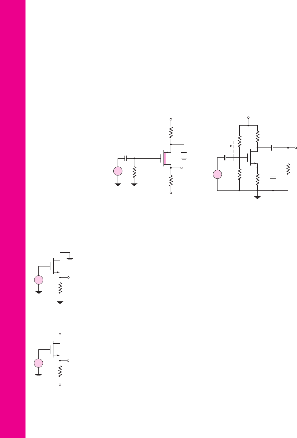
Section 4.3 The Common-Source Amplifier
4.13 Consider the circuit in Figure 4.14 in the text. The circuit parameters are
V
DD
= 3.3
V,
R
D
= 8
k
,
R
1
= 240
k
,
R
2
= 60
k
,and
R
Si
= 2
k
.
The transistor parameters are
V
TN
= 0.4
V,
k
n
= 100 μ
A/V
2
,
W/L = 80
,
and
λ = 0.02
V
−1
. (a) Determine the quiescent values
I
DQ
and
V
DSQ
.
(b) Find the small-signal parameters
g
m
and
r
o
. (c) Determine the small-signal
voltage gain.
4.14 A common-source amplifier, such as shown in Figure 4.14 in the text, has
parameters
r
o
= 100
k and
R
D
= 5
k. Determine the transconductance of
the transistor if the small-signal voltage gain is
A
v
=−10
. Assume
R
Si
= 0
.
4.15 For the NMOS common-source amplifier in Figure P4.15, the transistor
parameters are:
V
TN
= 0.8
V,
K
n
= 1
mA/V
2
, and
λ = 0
. The circuit para-
meters are
V
DD
= 5
V,
R
S
= 1
k
,
R
D
= 4
k
,
R
1
= 225
k
, and
R
2
= 175
k
. (a) Calculate the quiescent values
I
DQ
and
V
DSQ
. (b) Deter-
mine the small-signal voltage gain for
R
L
=∞
. (c) Determine the value of
R
L
that will reduce the small-signal voltage gain to 75 percent of the value
found in part (b).
R
2
v
i
R
in
R
1
C
C1
C
C2
R
D
V
DD
v
o
R
S
R
L
+
–
Figure P4.15
4.16 The parameters of the circuit shown in Figure P4.15 are
V
DD
= 12
V,
R
S
= 0.5
k
,
R
in
= 250
k
, and
R
L
= 10
k
. The transistor parameters are
V
TN
= 1.2
V,
K
n
= 1.5
mA/V
2
, and
λ = 0
. (a) Design the circuit such that
I
DQ
= 2
mA and
V
DSQ
= 5
V. (b) Determine the small-signal voltage gain.
4.17 Repeat Problem 4.15 if the source resistor is bypassed by a source capacitor
C
S
.
4.18 The ac equivalent circuit of a common-source amplifier is shown in Fig-
ure P4.18. The small-signal parameters of the transistor are
g
m
= 2
mA/V
and
r
o
=∞
. (a) The voltage gain is found to be
A
v
= V
o
/V
i
=−15
with
R
S
= 0
. What is the value of R
D
? (b) A source resistor R
S
is inserted.
Assuming the transistor parameters do not change, what is the value of R
S
if the voltage gain is reduced to
A
v
=−5
.
4.19 Consider the ac equivalent circuit shown in Figure P4.18. Assume
r
o
=∞
for the transistor. The small-signal voltage gain is
A
v
=−8
for the case
when
R
S
= 1
k. (a) When R
S
is shorted (
R
S
= 0
), the magnitude of the
voltage gain doubles. Assuming the small-signal transistor parameters do
not change, what are the values of g
m
and R
D
? (b) A new value of R
S
is
V
i
V
o
R
S
R
D
+
–
Figure P4.18
nea80644_ch04_205-284.qxd 06/12/2009 08:00 PM Page 269 F506 Tempwork:Dont' Del Rakesh:June:Rakesh 06-12-09:MHDQ134-04:
270 Part 1 Semiconductor Devices and Basic Applications
inserted into the circuit and the voltage gain becomes
A
v
=−10
. Using the
results of part (a), determine the value of R
S
.
4.20 The transistor in the common-source amplifier in Figure P4.20 has parame-
ters
V
TN
= 0.8
V,
k
n
= 100 μ
A/V
2
,
W/L = 50
, and
λ = 0.02
V
−1
. The
circuit parameters are
V
+
= 5
V,
V
−
=−5
V,
I
Q
= 0.5
mA, and
R
D
= 6
k
. (a) Determine
V
GSQ
and
V
DSQ
. (b) Find the small-signal volt-
age gain for
R
L
=∞
. (c) Repeat part (b) for
R
L
= 20
k
. (d) Repeat part
(b) for
R
L
= 6
k
.
V
+
V
–
v
i
v
o
R
G
=
200 kΩ
R
L
I
Q
R
D
C
C1
C
C2
C
S
+
–
Figure P4.20
v
i
v
o
R
G
R
L
=
40 kΩ
–5 V
+5 V
R
D
R
S
C
C
C
S
+
–
Figure P4.21
4.21 The parameters of the MOSFET in the circuit shown in Figure P4.21 are
V
TN
= 0.8
V,
K
n
= 0.85
mA/V
2
, and
λ = 0.02
V
−1
. (a) Determine
R
S
and
R
D
such that
I
DQ
= 0.1
mA and
V
DSQ
= 5.5
V. (b) Find the small-signal
transistor parameters. (c) Determine the small-signal voltage gain.
4.22 For the common-source amplifier in Figure P4.22, the transistor parameters
are
V
TN
=−0.8
V,
K
n
= 2
mA/V
2
, and
λ = 0
. The circuit parameters are
V
DD
= 3.3
V and
R
L
= 10
k
. (a) Design the circuit such that
I
DQ
= 0.5
mA and
V
DSQ
= 2
V. (b) Determine the small-signal voltage gain.
V
DD
v
i
v
o
R
G
= 1 MΩ
R
L
R
S
R
D
C
C1
C
C2
+
–
Figure P4.22
*4.23 The transistor in the common-source circuit in Figure P4.22 has the same
parameters as given in Problem 4.22. The circuit parameters are
V
DD
= 5
V
and
R
D
= R
L
= 2
k. (a) Find R
S
for
V
DSQ
= 2.5
V. (b) Determine the
small-signal voltage gain.
nea80644_ch04_205-284.qxd 06/13/2009 01:57 PM Page 270 F506 Hard disk:Desktop Folder:ALI-06-13-09:MHDQ134-04 Folder:MHDQ134-0
Chapter 4 Basic FET Amplifiers 271
*4.24 Consider the PMOS common-source circuit in Figure P4.24 with transistor
parameters
V
TP
=−2
V and
λ = 0
, and circuit parameters
R
D
= R
L
=
10 k. (a) Determine the values of K
p
and R
S
such that
V
SDQ
= 6
V.
(b) Determine the resulting value of
I
DQ
and the small-signal voltage gain.
(c) Can the values of K
p
and R
S
from part (a) be changed to achieve a larger
voltage gain, while still meeting the requirements of part (a)?
D4.25 For the common-source circuit in Figure P4.24, the bias voltages are
changed to
V
+
= 3
V and
V
−
=−3
V. The PMOS transistor parameters
are:
V
TP
=−0.5
V,
K
p
= 0.8
mA/V
2
, and
λ = 0
. The load resistor is
R
L
=
2k. (a) Design the circuit such that
I
DQ
= 0.25
mA and
V
SDQ
=
1.5 V.
(b) Determine the small-signal voltage gain
A
v
= v
o
/v
i
.
*D4.26 Design the common-source circuit in Figure P4.26 using an n-channel
MOSFET with
λ = 0
. The quiescent values are to be
I
DQ
= 6
mA,
V
GSQ
=
2.8 V, and
V
DSQ
= 10
V. The transconductance is
g
m
= 2.2
mA/V.
Let
R
L
= 1
k,
A
v
=−1
, and
R
in
= 100
k. Find R
1
, R
2
, R
S
, R
D
, K
n
,
and
V
TN
.
v
i
v
o
R
G
=
100 kΩ
R
L
R
D
R
S
C
C1
C
C2
+5 V
–5 V
C
S
+
–
Figure P4.24
R
2
v
i
R
in
R
1
C
C1
R
D
V
DD
= 18 V
v
o
R
S
R
L
C
C2
+
–
Figure P4.26
v
i
v
o
R
G
= 500 kΩ
R
L
R
D
I
Q
C
C1
C
C2
+9 V
–9 V
C
S
+
–
Figure P4.27
4.27 For the common-source amplifier shown in Figure P4.27, the transistor
parameters are
V
TP
=−1.2
V,
K
p
= 2
mA/V
2
, and
λ = 0.03
V
−1
. The
nea80644_ch04_205-284.qxd 06/12/2009 08:00 PM Page 271 F506 Tempwork:Dont' Del Rakesh:June:Rakesh 06-12-09:MHDQ134-04:
272 Part 1 Semiconductor Devices and Basic Applications
*D4.29 Design a common-source amplifier, such as that in Figure P4.29, to achieve
a small-signal voltage gain of at least
A
v
= v
o
/v
i
=−10
for
R
L
= 20 k
and
R
in
= 200 k
. Assume the Q-point is chosen at
I
DQ
= 1
mA and
V
DSQ
= 10
V. Let
V
TN
= 2
V, and
λ = 0
.
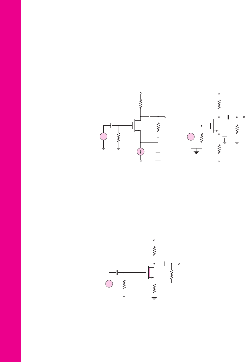
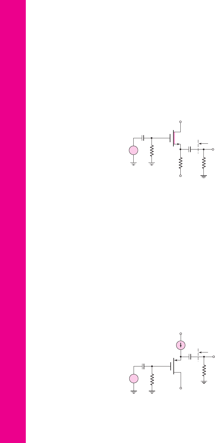
Section 4.4 The Source-Follower Amplifier
4.30 The small-signal parameters of an enhancement-mode MOSFET source
follower are
g
m
= 5
mA/V and
r
o
= 100
k
. (a) Determine the no-load
small-signal voltage gain and the output resistance. (b) Find the small-
signal voltage gain when a load resistance
R
S
= 5
k
is connected.
4.31 The open-circuit (
R
L
=∞
) voltage gain of the ac equivalent source-
follower circuit shown in Figure P4.31 is
A
v
= 0.98
. When R
L
is set to
1k
,
the voltage gain is reduced to
A
v
= 0.49
. What are the values of g
m
and r
o
?
4.32 Consider the source-follower circuit in Figure P4.31. The small-signal
parameters of the transistor are
g
m
= 2
mA/V and
r
o
= 25 k
. (a) Deter-
mine the open-circuit (
R
L
=∞
) voltage gain and output resistance. (b) If
R
L
= 2k
and the small-signal transistor parameters remain constant,
determine the voltage gain.
4.33 The source follower amplifier in Figure P4.33 is biased at
V
+
= 1.5
V
and
V
−
=−1.5
V. The transistor parameters are
V
TN
= 0.4
V,
k
n
= 100 μ
A/V
2
,
W/L = 80
, and
λ = 0.02
V
−1
. (a) The dc value of
v
O
is
to be zero volts. What is the current
I
DQ
and the required value of
V
GSQ
?
(b) Determine the small-signal voltage gain. (c) Find the output resistance
R
o
.
V
i
V
o
R
L
+
–
Figure P4.31
v
i
v
o
10 kΩ
V
–
V
+
+
–
Figure P4.33
v
i
v
o
R
G
= 200 kΩ
R
D
R
S
C
C
+10 V
–10 V
C
S
+
–
Figure P4.28
R
2
v
i
R
in
R
1
C
C1
R
D
V
DD
= 20 V
v
o
R
S
R
L
C
C2
C
S
+
–
Figure P4.29
drain resistor is
R
D
= 4
k
. (a) Determine
I
Q
such that
V
SDQ
= 5
V. (b) Find
the small-signal voltage gain for
R
L
=∞
. (c) Repeat part (b) for
R
L
=
8
k
.
D4.28 For the circuit shown in Figure P4.28, the transistor parameters are:
V
TP
= 0.8
V,
K
p
= 0.25
mA/V
2
, and
λ = 0
. (a) Design the circuit such that
I
DQ
= 0.5
mA and
V
SDQ
= 3
V. (b) Determine the small-signal voltage
gain
A
v
= v
o
/v
i
.
nea80644_ch04_205-284.qxd 06/12/2009 08:00 PM Page 272 F506 Tempwork:Dont' Del Rakesh:June:Rakesh 06-12-09:MHDQ134-04:
Chapter 4 Basic FET Amplifiers 273
4.35 The quiescent power dissipation in the circuit in Figure P4.35 is to be lim-
ited to 2.5 mW. The parameters of the transistor are
V
TN
= 0.6
V,
k
n
= 100 μ
A/V
2
, and
λ = 0.02
V
−1
. (a) Determine
I
Q
. (b) Determine
W/L
such that the output resistance is
R
o
= 0.5
k
. (c) Using the results of parts
(a) and (b), determine the small-signal voltage gain. (d) Determine the out-
put resistance if the transistor width-to-length ratio is
W/L = 100
.
4.36 The parameters of the circuit in Figure P4.36 are
R
S
= 4
k
,
R
1
= 850
k
,
R
2
= 350
k
, and
R
L
= 4
k
. The transistor parameters are
V
TP
=−1.2
V,
k
p
= 40 μ
A/V
2
,
W/L = 80
, and
λ = 0.05
V
−1
. (a) Determine
I
DQ
and
V
SDQ
. (b) Find the small-signal voltage gain
A
v
= v
o
/v
i
. (c) Determine the
small-signal circuit transconductance gain
A
g
= i
o
/v
i
. (d) Find the small-
signal output resistance
R
o
.
v
O
v
I
R
S
= 0.5 kΩ
V
DD
= 2.5 V
Figure P4.34
v
I
I
Q
V
DD
= 2.5 V
R
O
v
O
Figure P4.35
R
2
v
i
R
1
C
C1
R
S
V
DD
= 10 V
v
o
R
L
C
C2
i
i
i
o
R
o
+
–
Figure P4.36
+5 V
–5 V
v
i
C
C2
v
o
R
G
=
500 kΩ
R
L
=
4 kΩ
I
Q
C
C1
R
o
+
–
Figure P4.37
4.37 Consider the source follower circuit in Figure P4.37 with transistor parame-
ters
V
TN
= 0.8
V,
k
n
= 100 μ
A/V
2
,
W/L = 20
,and
λ = 0.02
V
−1
. (a) Let
I
Q
= 5
mA. (i) Determine the small-signal voltage gain. (ii) Find the output
resistance
R
o
. (b) Repeat part (a) for
I
Q
= 2
mA.
4.34 Consider the circuit in Figure P4.34. The transistor parameters are
V
TN
= 0.6
V,
k
n
= 100 μ
A/V
2
, and
λ = 0
. The circuit is to be designed
such that
V
DSQ
= 1.25
V and such that the small-signal voltage gain is
A
v
= 0.85
. (a) Find
I
DQ
. (b) Determine the width-to-length ratio of the tran-
sistor. (c) What is the required dc value of the input voltage?
nea80644_ch04_205-284.qxd 06/12/2009 08:00 PM Page 273 F506 Tempwork:Dont' Del Rakesh:June:Rakesh 06-12-09:MHDQ134-04:
274 Part 1 Semiconductor Devices and Basic Applications
4.38 For the source-follower circuit shown in Figure P4.37, the transistor parame-
ters are:
V
TN
= 1
V,
k
n
= 60 μA/V
2
, and
λ = 0
. The small-signal voltage
gain is to be
A
v
= v
o
/v
i
= 0.95
. (a) Determine the required width-to-length
ratio (W/L) for
I
Q
= 4
mA. (b) Determine the required I
Q
if (
W/L) = 60
.
*D4.39 In the source-follower circuit in Figure P4.39 with a depletion NMOS tran-
sistor, the device parameters are:
V
TN
=−2
V,
K
n
= 5
mA/V
2
, and
λ = 0.01 V
−1
. Design the circuit such that
I
DQ
= 5
mA. Find the small-
signal voltage gain
A
v
= v
o
/v
i
and the output resistance R
o
.
+5 V
–5 V
v
i
C
C2
R
S
v
o
R
G
=
200 kΩ
R
L
=
2 kΩ
C
C1
R
o
+
–
Figure P4.39
V
–
= –5 V
V
+
= 5 V
v
i
C
C 2
R
L
v
o
R
G
=
200 kΩ
I
Q
C
C1
R
o
+
–
Figure P4.42
4.40 For the circuit in Figure P4.39,
R
S
= 1
k
and the quiescent drain current
is
I
DQ
= 5
mA. The transistor parameters are
V
TN
=−2
V,
k
n
= 100 μ
A/V
2
, and
λ = 0.01
V
−1
. (a) Determine the transistor width-to-
length ratio. (b) Using the results of part (a), find the small-signal voltage
gain for
R
L
=∞
. (c) Find the small-signal output resistance
R
o
. (d) Using
the results of part (a), find
A
v
for
R
L
= 2
k
.
D4.41 For the source-follower circuit in Figure P4.39, the transistor parameters
are:
V
TN
=−2
V,
K
n
= 4
mA/V
2
, and
λ = 0
. Design the circuit such that
R
o
≤ 200
. Determine the resulting small-signal voltage gain.
4.42 The current source in the source-follower circuit in Figure P4.42 is
I
Q
= 10
mA and the transistor parameters are
V
TP
=−2
V,
K
p
= 5
mA/V
2
,
and
λ = 0.01
V
−1
. (a) Find the open circuit (
R
L
=∞
) small-signal voltage
gain. (b) Determine the small-signal output resistance
R
o
. (c) What value of
R
L
will reduce the small-signal voltage gain to
A
v
= 0.90
?
nea80644_ch04_205-284.qxd 06/12/2009 08:00 PM Page 274 F506 Tempwork:Dont' Del Rakesh:June:Rakesh 06-12-09:MHDQ134-04:

Chapter 4 Basic FET Amplifiers 275
V
DD
v
i
C
C2
R
S
R
L
R
G
v
o
C
C1
+
–
Figure P4.43
4.44 The transistor in the circuit in Figure P4.44 has parameters
V
TN
= 0.4
V,
K
n
= 0.5
mA/V
2
, and
λ = 0
. The circuit parameters are
V
DD
= 3
V and
R
i
= 300 k
. (a) Design the circuit such that
I
DQ
= 0.25
mA and
V
DSQ
= 1.5
V. (b) Determine the small-signal voltage gain and the output
resistance
R
o
.
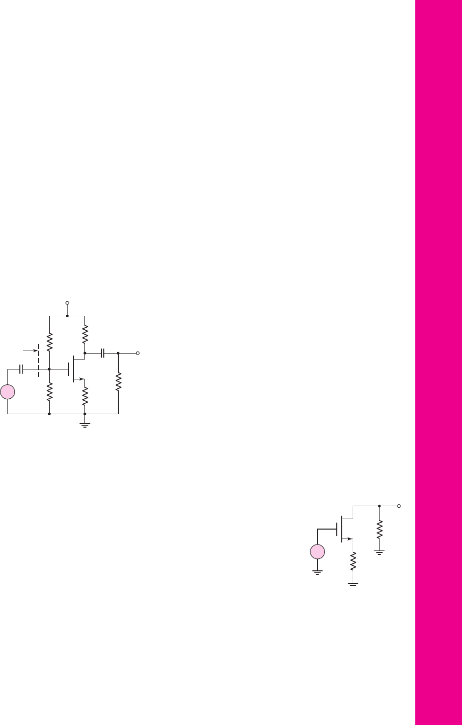
Section 4.5 The Common-Gate Configuration
4.45 Figure P4.45 is the ac equivalent circuit of a common-gate amplifier. The
transistor parameters are
V
TN
= 0.4
V,
k
n
= 100 μ
A/V
2
, and
λ = 0
. The
quiescent drain current is
I
DQ
= 0.25
mA. Determine the transistor
W/L
ratio and the value of
R
D
such that the small-signal voltage gain is
A
v
= V
o
/V
i
= 20
and the input resistance is
R
i
= 500
.
4.46 The transistor in the common-gate circuit in Figure P4.46 has the same
parameters that are given in Problem 4.45. The output resistance
R
o
is to
R
2
v
i
R
1
C
C1
R
S
V
DD
v
O
R
i
R
o
+
–
Figure P4.44
V
i
V
o
V
B
R
i
R
D
R
o
Figure P4.45
V
i
R
i
R
D
1.2 V = V
GSQ
V
DD
= 2.2 V
+
–
+
V
o
–
R
o
Figure P4.46
4.43 Consider the source-follower circuit shown in Figure P4.43. The most neg-
ative output signal voltage occurs when the transistor just cuts off. Show
that this output voltage v
o
(min) is given by
v
o
(min) =
−I
DQ
R
S
1 +
R
S
R
L
Show that the corresponding input voltage is given by
v
i
(min) =−
I
DQ
g
m
(1 + g
m
(R
S
R
L
))
nea80644_ch04_205-284.qxd 06/12/2009 08:00 PM Page 275 F506 Tempwork:Dont' Del Rakesh:June:Rakesh 06-12-09:MHDQ134-04:
276 Part 1 Semiconductor Devices and Basic Applications
4.48 For the common-gate circuit in Figure P4.48, the NMOS transistor parameters
are:
V
TN
= 1
V,
K
n
= 3
mA/V
2
, and
λ = 0
. (a) Determine
I
DQ
and
V
DSQ
.
(b) Calculate g
m
and r
o
. (c) Find the small-signal voltage gain
A
v
= v
o
/v
i
.
4.49 Consider the PMOS common-gate circuit in Figure P4.49. The transistor
parameters are:
V
TP
=−1V
,
K
p
= 0.5
mA/V
2
, and
λ = 0
. (a) Determine
R
S
and R
D
such that
I
DQ
= 0.75
mA and
V
SDQ
= 6
V. (b) Determine the
input impedance R
i
and the output impedance R
o
. (c) Determine the load
current i
o
and the output voltage
v
o
, if
i
i
= 5
sin
ω
t
μ
A.
C
C1
R
L
=
2 kΩ
R
G
=
50 kΩ
R
i
=
100 kΩ
R
D
i
i
v
o
R
S
C
G
C
C2
V
+
= +5 V
V
–
= –5 V
i
o
R
i
R
o
Figure P4.49
4.50 The transistor parameters of the NMOS device in the common-gate ampli-
fier in Figure P4.50 are
V
TN
= 0.4
V,
k
n
= 100 μ
A/V
2
, and
λ = 0
. (a) Find
R
D
such that
V
DSQ
= V
DS
(
sat
)
+0.25
V. (b) Determine the transistor
W/L
ratio such that the small-signal voltage gain is
A
v
= 6
. (c) What is the value
of
V
GSQ
?
4.51 The parameters of the circuit shown in Figure 4.32 are
V
+
= 3.3
V,
V
−
=−3.3
V,
R
G
= 50
k
,
R
L
= 4
k
,
R
Si
= 0
, and
I
Q
= 2
mA. The
transistor parameters are
V
TN
= 0.6
V,
K
n
= 4
mA/V
2
, and
λ = 0
. (a) Find
C
C
R
D
I
Q
=
2 mA
V
+
= 1.8 VV
–
= –1.8 V
V
o
V
i
+
–
Figure P4.50
V
i
V
o
10 kΩ 4 kΩ
+
–
R
i
Figure P4.47
C
C1
v
i
v
o
R
S
= 10 kΩ R
D
= 5 kΩ R
L
= 4 kΩ
C
C2
V
–
= –5 V
V
+
= +5 V
+
–
Figure P4.48
be 500
and the drain-to-source quiescent voltage is to be
V
DSQ
= V
DS
(sat) + 0.3
V. (a) What is the value of
R
D
? (b) What is the
quiescent drain current
I
DQ
? (c) Find the input resistance
R
i
. (d) Deter-
mine the small-signal voltage gain
A
v
= V
o
/V
i
.
4.47 The small-signal parameters of the NMOS transistor in the ac equivalent com-
mon-gate circuit shown in Figure P4.47 are
V
TN
= 0.4
V,
k
n
= 100 μ
A/V
2
,
W/L = 80
, and
λ = 0
. The quiescent drain current is
I
DQ
= 0.5
mA. Deter-
mine the small-signal voltage gain and the input resistance.
nea80644_ch04_205-284.qxd 06/12/2009 08:00 PM Page 276 F506 Tempwork:Dont' Del Rakesh:June:Rakesh 06-12-09:MHDQ134-04:

Chapter 4 Basic FET Amplifiers 277
R
D
such that
V
DSQ
= 3.5
V. (b) Determine the small-signal parameters
g
m
and
R
i
. (c) Find the small-signal voltage gain
A
v
.
4.52 For the common-gate amplifier in Figure 4.35 in the text, the PMOS tran-
sistor parameters are
V
TP
=−0.8
V,
K
p
= 2.5
mA/V
2
, and
λ = 0
. The cir-
cuit parameters are
V
+
= 3.3
V,
V
−
=−3.3
,
R
G
= 100
k
, and
R
L
= 4
k
. (a) Determine
R
S
and
R
D
such that
I
DQ
= 1.2
mA and
V
SDQ
= 3
V. (b) Determine the small-signal voltage gain
A
v
= v
o
/v
i
.
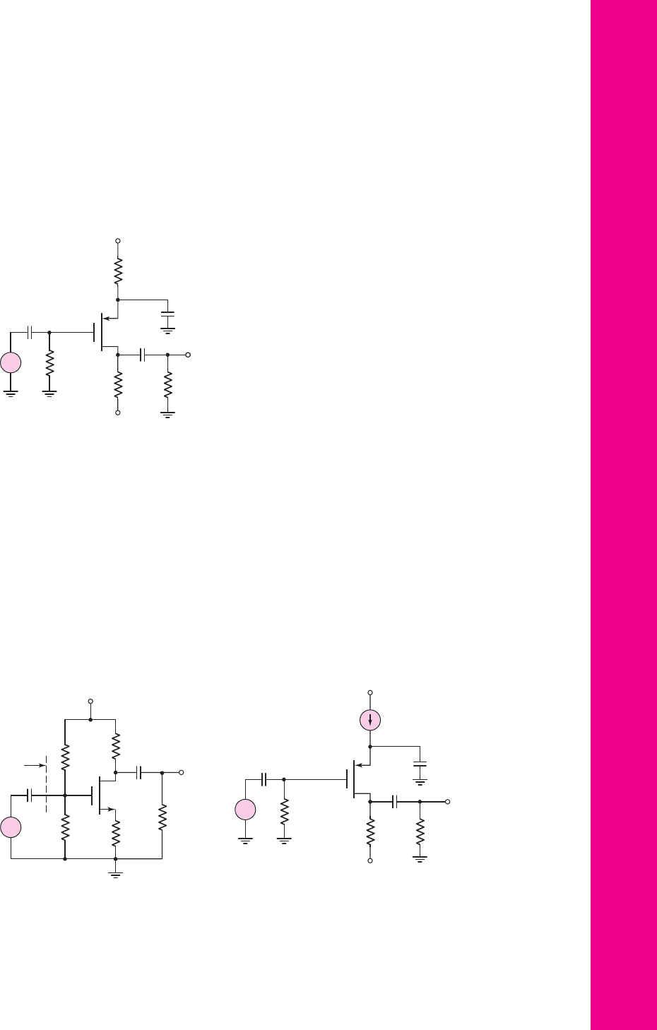
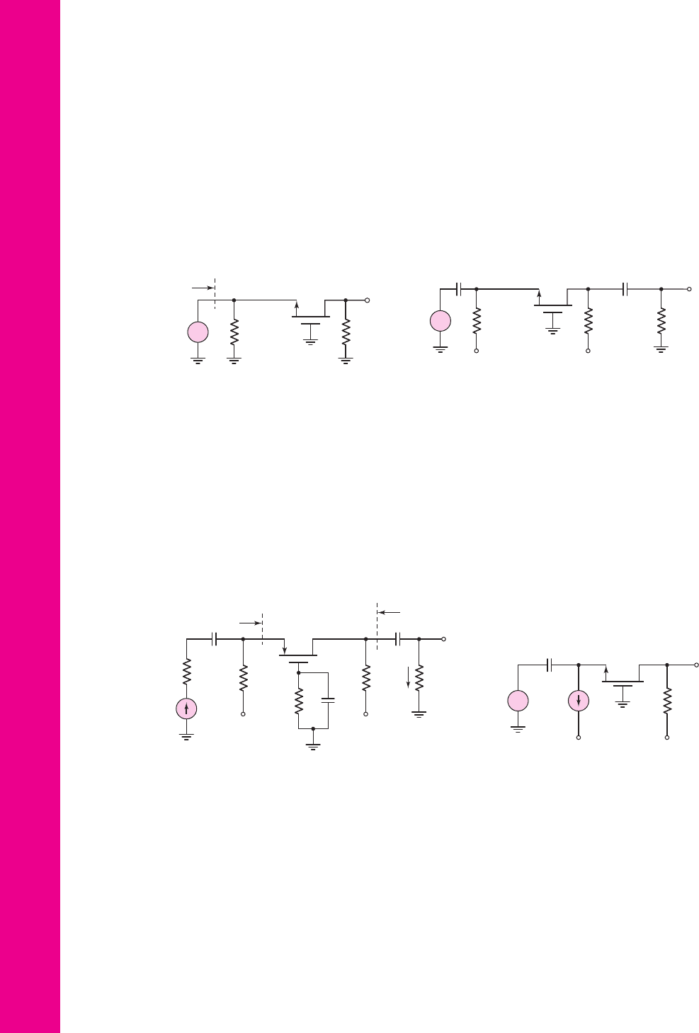
Section 4.7 Amplifiers with MOSFET Load Devices
4.53 Consider the NMOS amplifier with saturated load in Figure 4.39(a). The
transistor parameters are
V
TND
= V
TNL
= 0.6
V,
k
n
= 100 μ
A/V
2
,
λ = 0
,
and
(
W/L
)
L
= 1
. Let
V
DD
= 3.3
V. (a) Design the circuit such that the
small-signal voltage gain is
|
A
v
|
= 5
and the
Q
-point is in the center of the
saturation region. (b) Determine
I
DQ
and
V
DSDQ
.
4.54 For the NMOS amplifier with depletion load in Figure 4.43(a), the transis-
tor parameters are
V
TND
= 0.6V,V
TNL
=−0.8
V,
K
nD
= 1.2
mA/V
2
,
K
nL
= 0.2
mA/V
2
, and
λ
D
= λ
L
= 0.02
V
−1
. Let
V
DD
= 5
V. (a) Deter-
mine the transistor voltages at the transition points A and B. (b) Find
V
GSDQ
and
V
DSDQ
such that the
Q
-point is in the middle of the saturation region.
(c) Determine
I
DQ
. (d) Find the small-signal voltage gain.
4.55 Consider a saturated load device in which the gate and drain of an
enhancement-mode MOSFET are connected together. The transistor drain
current becomes zero when
V
DS
= 0.6
V. (a) At
V
DS
= 1.5
V, the drain
current is 0.5 mA. Determine the small-signal resistance at this operating
point. (b) What is the drain current and small-signal resistance at
V
DS
= 3
V?
4.56 The parameters of the transistors in the circuit in Figure P4.56 are
V
TND
=
−1V
,
K
nD
= 0.5
mA/V
2
for transistor M
D
, and
V
TNL
=+1
V,
K
nL
=
30
μ
A/V
2
for transistor M
L
. Assume
λ = 0
for both transistors. (a) Calcu-
late the quiescent drain current I
DQ
and the dc value of the output voltage.
(b) Determine the small-signal voltage gain
A
v
= v
o
/v
i
about the Q-point.
4.57 A source-follower circuit with a saturated load is shown in Figure P4.57.
The transistor parameters are
V
TND
= 1
V,
K
nD
= 1
mA/V
2
for M
D
, and
V
TNL
= 1
V,
K
nL
= 0.1
mA/V
2
for M
L
. Assume
λ = 0
for both transistors.
Let
V
DD
= 9
V. (a) Determine V
GG
such that the quiescent value of
v
DSL
is
4 V. (b) Show that the small-signal open-circuit
(R
L
=∞)
voltage gain
about this Q-point is given by
A
v
= 1/[1 +
√
K
nL
/K
nD
]
. (c) Calculate the
small-signal voltage gain for
R
L
= 4
k
.
V
DD
= 10 V
v
O
v
i
M
L
M
D
+
–
Figure P4.56
R
L
v
i
C
C
v
o
V
DD
M
L
+
–
V
GG
+
–
v
DSL
M
D
R
o
+
–
Figure P4.57
nea80644_ch04_205-284.qxd 06/12/2009 08:00 PM Page 277 F506 Tempwork:Dont' Del Rakesh:June:Rakesh 06-12-09:MHDQ134-04: