Neamen D. Microelectronics: Circuit Analysis and Design
Подождите немного. Документ загружается.

318 Part 1 Semiconductor Devices and Basic Applications
or
5 = (1.25)(2) + 0.7 + (0.0205)R
B
+(−2)
which yields
R
B
= 185 k
.
Solution (ideal load line): The load line equation is
V
EC
= V
+
− I
E
R
E
= V
+
− I
C
1 + β
β
R
E
or
V
EC
= 5 − I
C
61
60
(2) = 5 − I
C
(2.03)
The load line, using the nominal value of
R
E
, and the calculated Q-point are shown
in Figure 5.37(a).
Trade-offs: As shown in Appendix C, a standard resistor value of 185 k
is not
available. We will pick a value of 180 k
. We will consider
R
B
and
R
E
resistor tol-
erances of
±10
percent.
The quiescent collector current is given by
I
CQ
= β
V
+
− V
EB
(on) − V
BB
R
B
+(1 +β)R
E
= (60)
6.3
R
B
+(61)R
E
and the load line is given by
V
EC
= V
+
− I
C
1 + β
β
R
E
= 5 −
61
60
I
C
R
E
The extreme values of
R
E
are:
2k − 10% = 1.8k 2k + 10% = 2.2k.
I
CQ
= 1.23 mA
I
BQ
= 20.5 mA
012345
0.5
1.0
1.5
2.0
2.5
V
ECQ
= 2.5 V
v
EC
(V)
i
C
(mA)
Q-point
= 2.46 mA
I
C
(max) =
5
2.03
R
E
= 1.8 kΩ
R
E
= 2.2 kΩ
1.5 2.0 2.5 3.0 3.5
0.6
1.0
1.4
1.8
2.2
V
EC
(V)
I
C
(mA)
Ideal Q-point
Load lines
R
E
= 2 kΩ
R
B
= 162 kΩ
R
B
= 198 kΩ
(a) (b)
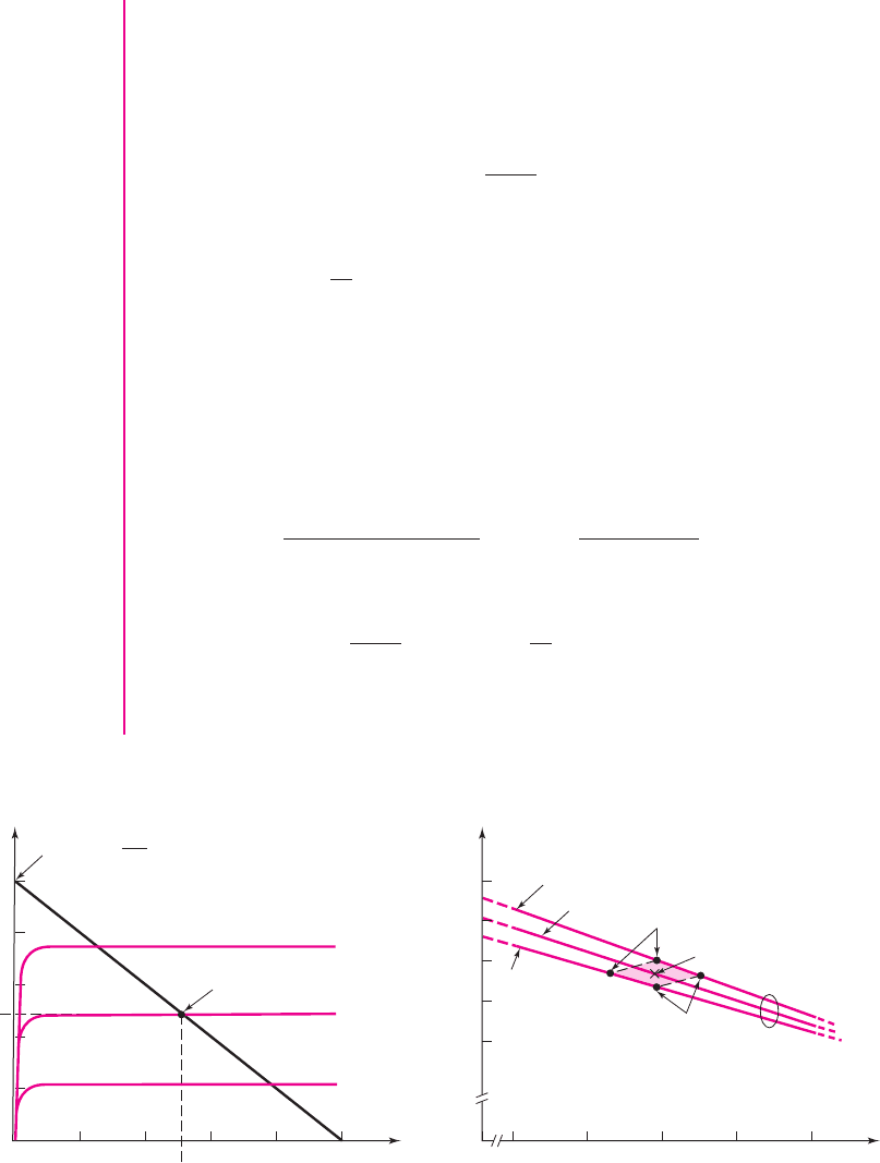
Figure 5.37 (a) Load line and Q-point value for the ideal designed circuit shown in
Figure 5.36 used in Example 5.9; (b) load lines and Q-point values for the extreme tolerance
values of resistors
nea80644_ch05_285-368.qxd 06/12/2009 08:42 PM Page 318 F506 Tempwork:Dont' Del Rakesh:June:Rakesh 06-12-09:MHDQ134-05:

Chapter 5 The Bipolar Junction Transistor 319
The extreme values of R
B
are:
180 k − 10% = 162 k 180 k + 10% = 198 k.
The Q-point values for the extreme values of
R
B
and
R
E
are given in the following
table.
R
E
R
B
1.8 k 2.2 k
162 k
I
CQ
= 1.39
mA
I
CQ
= 1.28
mA
V
ECQ
= 2.46
V
V
ECQ
= 2.14
V
198 k
I
CQ
= 1.23
mA
I
CQ
= 1.14
mA
V
ECQ
= 2.75
V
V
ECQ
= 2.45
V
Figure 5.37(b) shows the Q-points for the various possible extreme values of
emitter and base resistances. The shaded area shows the region in which the Q-point
will occur over the range of resistor values.
Comment: This example shows that an ideal Q-point can be determined based on a
set of specifications, but, because of resistor tolerance, the actual Q-point will vary
over a range of values. Other examples will consider the tolerances involved in
transistor parameters.
EXERCISE PROBLEM
Ex 5.9: The circuit elements in Figure 5.36(a) are
V
+
= 5
V,
V
BB
=−2
V,
R
E
= 2
k
, and
R
B
= 180
k
. Assume
V
EB
(on) = 0.7
V. Plot the Q-point
on the load line for (a)
β = 40
, (b)
β = 60
, (c)
β = 100
, and (d)
β = 150
.
(Ans. (a)
I
CQ
= 0.962
mA, (b)
I
CQ
= 1.25
mA, (c)
I
CQ
= 1.65
mA, (d)
I
CQ
=
1.96 mA)
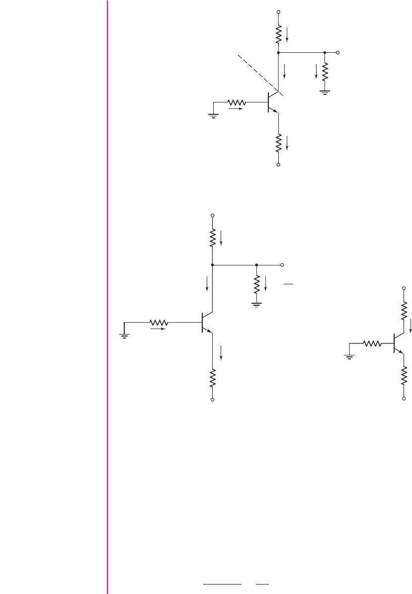
EXAMPLE 5.10
Objective: Calculate the characteristics of an npn bipolar transistor circuit with a
load resistance. The load resistance can represent a second transistor stage connected
to the output of a transistor circuit.
For the circuit shown in Figure 5.38(a), the transistor parameters are:
V
BE
(on) = 0.7
V, and
β = 100
.
Solution (Q-Point Values): Kirchhoff’s voltage law equation around the B–E loop
yields
I
B
R
B
+ V
BE
(on) + I
E
R
E
+ V
−
= 0
Again assuming
I
E
= (1 +β)I
B
, we find
I
B
=
−(V
−
+ V
BE
(on))
R
B
+(1 +β)R
E
=
−(−5 + 0.7)
10 + (101)(5)
⇒ 8.35 μA
The collector and emitter currents are
I
C
= β I
B
= (100)(8.35 μA) ⇒ 0.835 mA
nea80644_ch05_285-368.qxd 06/12/2009 08:42 PM Page 319 F506 Tempwork:Dont' Del Rakesh:June:Rakesh 06-12-09:MHDQ134-05:
320 Part 1 Semiconductor Devices and Basic Applications
and
I
E
= (1 +β)I
B
= (101)(8.35 μA) ⇒ 0.843 mA
At the collector node, we can write
I
C
= I
1
− I
L
=
V
+
− V
O
R
C
−
V
O
R
L
R
C
= 5 kΩ
R
B
= 10 kΩ
R
E
= 5 kΩ
R
L
= 5 kΩ
V
+
= +12 V
Make Thevenin
equivalent circuit
for load line
V
–
= –5 V
I
E
+
–
+
–
V
BE
I
B
I
L
I
1
I
C
V
O
V
CE
R
C
= 5 kΩ
R
B
= 10 kΩ
R
E
= 5 kΩ
R
L
= 5 kΩ
+12 V
–5 V
I
E
+
–
+
–
0.7 V
I
B
= 8.35
m
A
I
E
= (1 +
b
) I
B
= 0.843 mA
I
C
= bI
B
= 0.835 mA
= 0.782 mA
I
1
= I
C
+ I
L
= 1.63 mA
I
L
=
V
O
R
L
V
O
= 3.91 V
V
CE
= 4.7 V
V
TH
= 6 V
R
E
= 5 kΩ
R
B
= 10 kΩ
R
TH
= 2.5 kΩ
V
C
E
–5 V
I
C
–
+
(a)
(b) (c)
Figure 5.38 Circuit for Example 5.10: (a) circuit; (b) circuit showing current and voltage
values; and (c) Thevenin equivalent circuit
nea80644_ch05_285-368.qxd 06/12/2009 08:42 PM Page 320 F506 Tempwork:Dont' Del Rakesh:June:Rakesh 06-12-09:MHDQ134-05:
Chapter 5 The Bipolar Junction Transistor 321
or
0.835 =
12 − V
O
5
−
V
O
5
Solving for
V
O
, we find
V
O
= 3.91
V. The currents are then
I
1
= 1.62
mA and
I
L
= 0.782
mA. Referring to Figure 5.38(b), the collector–emitter voltage is
V
CE
= V
O
− I
E
R
E
−(−5) = 3.91 −(0.843)(5) − (−5) = 4.70 V
Solution (Load Line): The load line equation for this circuit is not as straightforward
as for previous circuits. The easiest approach to finding the load line is to make a
“Thevenin equivalent circuit” of
R
L
,
R
C
, and
V
+
, as indicated in Figure 5.38(b).
(Thevenin equivalent circuits are also covered later in this chapter, in Section 5.4.)
The Thevenin equivalent resistance is
R
TH
= R
L
R
C
= 55 = 2.5k
and the Thevenin equivalent voltage is
V
TH
=
R
L
R
L
+ R
C
· V
+
=
5
5 + 5
· (12) = 6V
The equivalent circuit is shown in Figure 5.38(c). The Kirchhoff voltage law equa-
tion around the C–E loop is
V
CE
= (6 −(−5)) − I
C
R
TH
− I
E
R
E
= 11 − I
C
(2.5) − I
C
101
100
· (5)
or
V
CE
= 11 − I
C
(7.55)
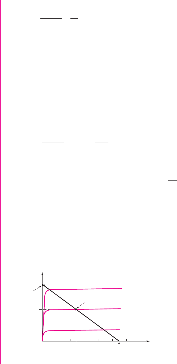
The load line and the calculated Q-point values are shown in Figure 5.39.
Comment: Remember that the collector current, determined from
I
C
= β I
B
, is the
current into the collector terminal of the transistor; it is not necessarily the current in
the collector resistor
R
C
.
I
CQ
= 0.835 mA
2 4 6 8 10 12
0.5
1.0
1.50
1.46
V
CEQ
= 4.70 V
v
CE
(V)
I
BQ
= 8.35
m
A
i
C
(mA)
Q-point
11
Figure 5.39 Load line and Q-point for the circuit shown in Figure 5.38(a) for Example 5.10
nea80644_ch05_285-368.qxd 06/12/2009 08:42 PM Page 321 F506 Tempwork:Dont' Del Rakesh:June:Rakesh 06-12-09:MHDQ134-05:
+
–
+
–
V
BB
= 4 V V
CC
= 5 V
I
E
R
E
I
C
R
C
= 1 kΩ
Figure 5.40 Figure for Exercise Ex 5.10
322
Part 1 Semiconductor Devices and Basic Applications
EXERCISE PROBLEM
Ex 5.10: For the transistor shown in the circuit of Figure 5.40, the common-base
current gain is
α = 0.9920
. Determine
R
E
such that the emitter current is limited
to
I
E
= 1.0
mA. Also determine
I
B
,
I
C
, and
V
BC
. (Ans.
R
E
= 3.3
k
,
I
C
= 0.992
mA,
I
B
= 8.0 μ
A,
V
BC
= 4.01
V)
Test Your Understanding
TYU 5.11 For the circuit shown in Figure 5.41, determine
I
E
,
I
B
,
I
C
, and
V
CE
,if
β = 75
. (Ans.
I
B
= 15.1 μ
A,
I
C
= 1.13
mA,
I
E
= 1.15
mA,
V
CE
= 6.03
V)
TYU 5.12 Assume
β = 120
for the transistor in Figure 5.42. Determine
R
E
such that
V
CE
= 2.2
V. (Ans.
R
E
= 154 )
+
–+
–
V
BB
= 2 V V
CC
= 8 V
I
E
R
C
= 2.5 kΩR
E
= 1 kΩ
R
B
= 10 kΩ
Figure 5.41 Figure for Exercise TYU 5.11
+
–
V
BB
= 5 V
+5 V
R
E
R
B
= 10 kΩ
Figure 5.42 Figure for
Exercise TYU 5.12
TYU 5.13
For the transistor in Figure 5.43, assume
β = 90
. (a) Determine
V
BB
such
that
I
E
= 1.2
mA. (b) Find
I
C
and
V
EC
. (Ans. (a)
V
BB
= 2.56
V; (b)
I
C
= 1.19
mA,
V
EC
= 3.8
V)
COMPUTER ANALYSIS EXERCISE
PS 5.3: Verify the common-base circuit analysis in Test Your Understanding Ex-
ercise TYU 5.11 with a PSpice simulation. Use a standard transistor.
+
–
V
BB
–5 V
R
B
= 50 kΩ
R
E
= 1 kΩ
I
E
Figure 5.43 Figure for
Exercise TYU 5.13
nea80644_ch05_285-368.qxd 06/12/2009 08:42 PM Page 322 F506 Tempwork:Dont' Del Rakesh:June:Rakesh 06-12-09:MHDQ134-05:

Chapter 5 The Bipolar Junction Transistor 323
5.3 BASIC TRANSISTOR APPLICATIONS
Objective: • Examine three applications of bipolar transistor circuits:
a switch circuit, digital logic circuit, and an amplifier circuit.
Transistors can be used to: switch currents, voltages, and power; perform digital
logic functions; and amplify time-varying signals. In this section, we consider the
switching properties of the bipolar transistor, analyze a simple transistor digital logic
circuit, and then show how the bipolar transistor is used to amplify time-varying
signals.
Switch
Figure 5.44 shows a bipolar circuit called an inverter, in which the transistor in the
circuit is switched between cutoff and saturation. The load, for example, could be a
motor, a light-emitting diode or some other electrical device. If
v
I
< V
BE
(on), then
i
B
= i
C
= 0
and the transistor is cut off. Since
i
C
= 0
, the voltage drop across the
load is zero, so the output voltage is
v
O
= V
CC
. Also, since the currents in the tran-
sistor are zero, the power dissipation in the transistor is zero. If the load were a motor,
the motor would be off with zero current. Likewise, if the load were a light-emitting
diode, the light output would be zero with zero current.
If we let
v
I
= V
CC
and if the ratio of
R
B
to
R
C
, where
R
C
is the effective resis-
tance of the load, is less than
β
, then the transistor is usually driven into saturation,
which means that
i
B
∼
=
v
I
− V
BE
(on)
R
B
(5.34)
i
C
= I
C
(sat) =
V
CC
− V
CE
(sat)
R
C
(5.35)
and
v
O
= V
CE
(sat)
(5.36)
5.3.1
V
CC
v
CE
v
BE
v
I
v
O
i
C
R
B
i
B
+
+
–
–
Load
Figure 5.44 An npn bipolar inverter circuit used as a switch
nea80644_ch05_285-368.qxd 06/12/2009 08:42 PM Page 323 F506 Tempwork:Dont' Del Rakesh:June:Rakesh 06-12-09:MHDQ134-05:
324 Part 1 Semiconductor Devices and Basic Applications
In this case, a collector current is induced that would turn on the motor or the LED,
depending on the type of load.
Equation (5.34) assumes that the B–E voltage can be approximated by the turn-
on voltage. This approximation will be modified slightly when we discuss bipolar
digital logic circuits in Chapter 17.
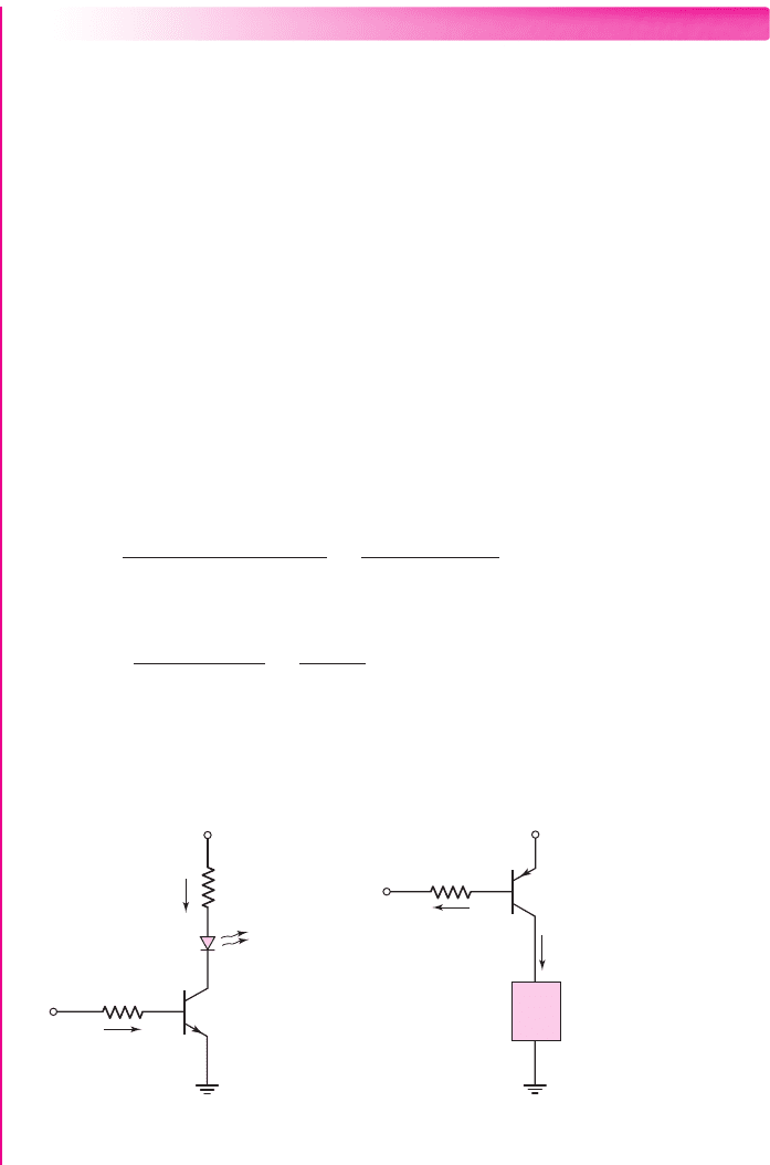
EXAMPLE 5.11
Objective: Calculate the appropriate resistance values and transistor power dissipa-
tion for the two inverter switching configurations shown in Figure 5.45.
Specifications (Figure 5.45(a)): The transistor in the inverter circuit in Figure
5.45(a) is used to turn the light-emitting diode (LED) on and off. The required LED
current is
I
C1
= 12
mA to produce the specified output light. Assume transistor pa-
rameters of
β = 80
,
V
BE
(
on
)
= 0.7
V, and
V
CE
(
sat
)
= 0.2
V, and assume the diode
cut-in voltage is
V
γ
= 1.5
V. [Note: LEDs are fabricated with compound semicon-
ductor materials and have a larger cut-in voltage compared to silicon diodes.]
Specifications (Figure 5.45(b)): The inverter circuit in Figure 5.45(b) uses a pnp
transistor. In this case, one side of the load (for example a motor) can be connected
to ground potential. The required load current is
I
C2
= 5
A. Assume transistor para-
meters of
β = 40,V
EB
(
on
)
= 0.7
V, and
V
EC
(
sat
)
= 0.2
V.
Solution (Figure 5.45(a)): For
v
I1
= 0
, transistor
Q
1
is cut off so that
I
B1
= I
C2
= 0
and the LED is also off.
For
v
I1
= 5
V, we require
I
C1
= 12
mA and want the transistor to be driven into
saturation. Then
R
1
=
V
+
−(V
γ
+ V
CE
(sat))
I
C1
=
5 − (1.5 +0.2)
12
⇒ R
1
= 275
We may let
I
C1
/I
B1
= 40
. Then
I
B1
= 12/40 = 0.3
mA. Now
R
B1
=
v
I1
− V
BE
(on)
I
B1
=
5 − 0.7
0.3
= 14.3k
The power dissipation in
Q
1
is
P
1
= I
B1
V
BE
(on) + I
C1
V
CE
(sat) = (0.3)(0.7) +(12)(0.2) = 2.61 mW
Figure 5.45 Figures for Example 5.11
Light
output
LED
V
+
= 5 V
I
C1
I
B1
R
1
R
B1
Q
1
v
I1
(a)
v
I2
R
B2
Q
2
I
B2
I
C2
V
+
= 12 V
Load
(b)
nea80644_ch05_285-368.qxd 06/12/2009 08:42 PM Page 324 F506 Tempwork:Dont' Del Rakesh:June:Rakesh 06-12-09:MHDQ134-05:

Chapter 5 The Bipolar Junction Transistor 325
Solution (Figure 5.45(b)):
For
v
I2
= 12
V, transistor
Q
2
is cut off so that
I
B2
= I
C2
= 0
and the voltage across the load is zero.
For
v
I2
= 0
, transistor
Q
2
is to be driven into saturation so that
V
EC2
=
V
EC
(
sat
)
= 0.2
V. The voltage across the load is 11.8 V, the current is 5 A, which
means the effective load resistance is
2.36
If we let
I
C2
/I
B2
= 20
, then
I
B2
= 5/20 = 0.25
A. Now
R
B2
=
V
+
− V
EB
(on) − v
I2
I
B2
=
12 − 0.7 −0
0.25
= 45.2
The power dissipation in transistor
Q
2
is
P
2
= I
B2
V
EB
(on) + I
C2
V
EC
(sat) = (0.25)(0.7) +(5)(0.2) = 1.175 W
Comment: As with most electronic circuit designs, there are some assumptions that
need to be made. The assumption to let
I
C
/I
B
= (1/2)β
in each case ensures that
each transistor will be driven into saturation even if variations in circuit parameters
occur. At the same time, base currents are limited to reasonable values.
We may note that for the circuit in Figure 5.45(a), a base current of only 0.3 mA
induces a load current of 12 mA. For the circuit in Figure 5.45(b), a base current of
only 0.25 A induces a load current of 5 A. The advantage of transistor switches is that
large load currents can be switched with relatively small base currents.
EXERCISE PROBLEM
Ex 5.11: (a) Redesign the LED circuit in Figure 5.45(a) such that
I
C1
= 15
mA and
I
C1
/I
B1
= 50
for
v
I
= 5
V. Use the same
Q
1
transistor parameters given in Exam-
ple 5.11. (b) Redesign the circuit in Figure 5.45(b) such that
I
C2
= 2
A and
I
C2
/I
B2
= 25
for
v
I
= 0
. Use the same
Q
2
transistor parameters as given in Exam-
ple 5.11. (Ans. (a)
R
1
= 220
,
R
B1
= 14.3
k
; (b)
R
B2
= 141 )
When a transistor is biased in saturation, the relationship between the collector
and base currents is no longer linear. Consequently, this mode of operation cannot be
used for linear amplifiers. On the other hand, switching a transistor between cutoff
and saturation produces the greatest change in output voltage, which is especially
useful in digital logic circuits, as we will see in the next section.
Digital Logic
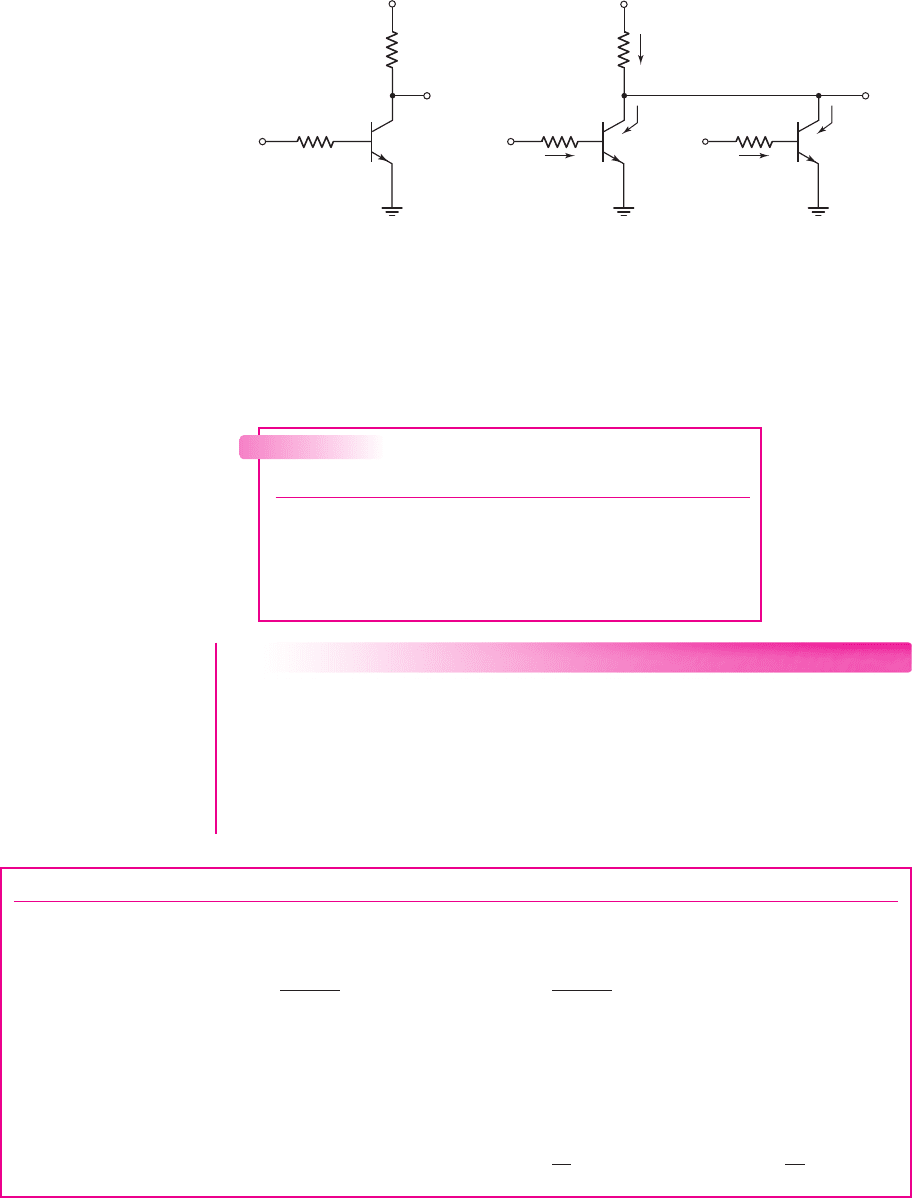
Consider the simple transistor inverter circuit shown in Figure 5.46(a). If the input
V
I
is approximately zero volts, the transistor is cut off and the output
V
O
is high and
equal to
V
CC
. If, on the other hand, the input is high and equal to
V
CC
, the transistor
can be driven into saturation, in which case the output is low and equal to
V
CE
(
sat
)
.
Now consider the case when a second transistor is connected in parallel, as
shown in Figure 5.46(b). When the two inputs are zero, both transistors
Q
1
and
Q
2
are in cutoff, and
V
O
= 5
V. When
V
1
= 5
V and
V
2
= 0
, transistor
Q
1
can be driven
into saturation, and
Q
2
remains in cutoff. With
Q
1
in saturation, the output voltage is
V
O
= V
CE
(sat)
∼
=
0.2 V. If we reverse the input voltages so that
V
1
= 0
and
V
2
= 5
V,
then
Q
1
is in cutoff,
Q
2
can be driven into saturation, and
V
O
= V
CE
(sat)
∼
=
0.2 V. If
both inputs are high, meaning
V
1
= V
2
= 5
V, then both transistors can be driven into
saturation, and
V
O
= V
CE
(sat)
∼
=
0.2 V.
5.3.2
nea80644_ch05_285-368.qxd 06/12/2009 08:42 PM Page 325 F506 Tempwork:Dont' Del Rakesh:June:Rakesh 06-12-09:MHDQ134-05:
326 Part 1 Semiconductor Devices and Basic Applications
Table 5.2 shows these various conditions for the circuit in Figure 5.46(b). In a
positive logic system, meaning that the larger voltage is a logic 1 and the lower volt-
age is a logic 0, this circuit performs the NOR logic function. The circuit of Fig-
ure 5.46(b) is then a two-input bipolar NOR logic circuit.
EXAMPLE 5.12
Objective: Determine the currents and voltages in the circuit shown in Fig-
ure 5.46(b).
Assume the transistor parameters are:
β = 50
,
V
BE
(on) = 0.7
V, and
V
CE
(sat) =
0.2 V. Let
R
C
= 1
k
and
R
B
= 20
k
. Determine the currents and output voltage
for various input conditions.
Solution: The following table indicates the equations and results for this example.
V
CC
= 5 V V
CC
= 5 V
R
C
R
C
R
B
R
B
R
B
I
B1
I
B2
I
C1
I
R
V
2
Q
1
I
C2
Q
2
V
I
V
1
V
O
V
O
(a) (b)
Figure 5.46 A bipolar (a) inverter circuit and (b) NOR logic gate
Table 5.2 The bipolar NOR logic circuit response
V
1
(V) V
2
(V) V
O
(V)
005
5 0 0.2
0 5 0.2
5 5 0.2
Condition V
O
I
R
Q
1
Q
2
V
1
= 0
,5 V0
I
B1
= I
C1
= 0 I
B2
= I
C2
= 0
V
2
= 0
V
1
= 5
V, 0.2 V
5 − 0.2
1
= 4.8
mA
I
B1
=
5 − 0.7
20
I
B2
= I
C2
= 0
V
2
= 0
= 0.215
mA
I
C1
= I
R
= 4.8
mA
V
1
= 0
, 0.2 V 4.8 mA
I
B1
= I
C1
= 0 I
B2
= 0.215
mA
V
2
= 5
V
I
C2
= I
R
= 4.8
mA
V
1
= 5
V, 0.2 V 4.8 mA
I
B1
= 0.215
mA
I
B2
= 0.215
mA
V
2
= 5
V
I
C1
=
I
R
2
= 2.4
mA
I
C2
=
I
R
2
= 2.4
mA
nea80644_ch05_285-368.qxd 06/12/2009 08:42 PM Page 326 F506 Tempwork:Dont' Del Rakesh:June:Rakesh 06-12-09:MHDQ134-05:
Chapter 5 The Bipolar Junction Transistor 327
Comment: In this example, we see that whenever a transistor is conducting, the
ratio of collector current to base current is always less than
β
. This shows that
the transistor is in saturation, which occurs when either
V
1
or
V
2
is 5 V.
EXERCISE PROBLEM
Ex 5.12: The transistor parameters in the circuit in Figure 5.46(b) are:
β = 40
,
V
BE
(on) = 0.7
V, and
V
CE
(sat) = 0.2
V. Let
R
C
= 600
and
R
B
= 950
.
Determine the currents and output voltage for: (a)
V
1
= V
2
= 0
; (b)
V
1
= 5V
,
V
2
= 0
; and (c)
V
1
= V
2
= 5
V. (Ans. (a) The currents are zero,
V
O
= 5
V;
(b)
I
B2
= I
C2
= 0
,
I
B1
= 4.53
mA,
I
C1
= I
R
= 8
mA,
V
O
= 0.2
V; (c)
I
B1
=
I
B2
= 4.53
mA,
I
C1
= I
C2
= 4mA= I
R
/2
,
V
O
= 0.2
V)
This example and the accompanying discussion illustrate that bipolar transistor
circuits can be configured to perform logic functions. In Chapter 17, we will see that
this circuit can experience loading effects when load circuits or other digital logic cir-
cuits are connected to the output. Therefore, logic circuits must be designed to mini-
mize or eliminate such loading effects.
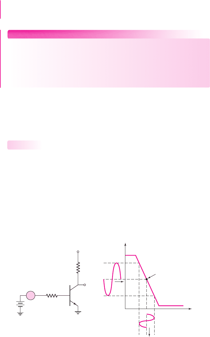
Amplifier
The bipolar inverter circuit can also be used to amplify a time-varying signal. Fig-
ure 5.47(a) shows an inverter circuit including a time-varying voltage source
v
I
in
the base circuit. The voltage transfer characteristics are shown in Figure 5.47(b). The
dc voltage source
V
BB
is used to bias the transistor in the forward-active region. The
Q-point is shown on the transfer characteristics.
The voltage source
v
I
introduces a time-varying signal on the input. A change
in the input voltage then produces a change in the output voltage. These time-varying
input and output signals are shown in Figure 5.47(b). If the magnitude of the slope of
the transfer characteristics is greater than unity, then the time-varying output signal
will be larger than the time-varying input signal—thus an amplifier.
5.3.3
+
+
–
–
Q-point
Time
Time
R
C
V
+
R
B
V
BB
V
BB
v
O
v
O
Δv
O
Δv
I
Δv
I
v
I
(a) (b)
Figure 5.47 (a) A bipolar inverter circuit to be used as a time-varying amplifier; (b) the
voltage transfer characteristics
nea80644_ch05_285-368.qxd 06/12/2009 08:42 PM Page 327 F506 Tempwork:Dont' Del Rakesh:June:Rakesh 06-12-09:MHDQ134-05: