Neamen D. Microelectronics: Circuit Analysis and Design
Подождите немного. Документ загружается.

328 Part 1 Semiconductor Devices and Basic Applications
EXAMPLE 5.13
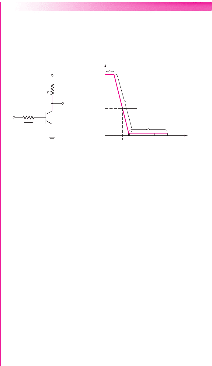
Objective: Determine the amplification factor for the circuit given in Figure 5.48(a).
The transistor parameters are
β = 120
,
V
BE
(on) = 0.7
V, and
V
A
=∞
.
DC Solution: The voltage transfer characteristics were developed in Example 5.6 for
this same circuit. The voltage transfer curve is repeated for convenience in Figure
5.48(b).
i
C
R
B
= 150 kΩ
R
C
= 5 kΩ
v
I
(V)
v
O
(V)
5
2.6
0.2
0 0.7 1.9
1.3
5
V
+
= 5 V
i
B
v
O
v
I
Cutoff
Forward-active
mode
Saturation
Q-point
(a) (b)
Figure 5.48 (a) A bipolar inverter used as an amplifier; (b) the inverter voltage transfer
characteristics
For
0.7 ≤ v
I
≤ 1.9
V, the transistor is biased in the forward-active mode and the
output voltage is given by
v
O
= 7.8 −4v
I
Now bias the transistor in the center of the active region with an input voltage of
v
I
= V
BB
= 1.3
V. The dc output voltage is
v
O
= 2.6
V. The Q-point is shown on the
transfer characteristics.
AC Solution: From
v
O
= 7.8 −4v
I
, we can find the change in output voltage with
respect to a change in input voltage. We find
v
O
=−4v
I
The voltage gain is then
A
v
=
v
O
v
I
=−4
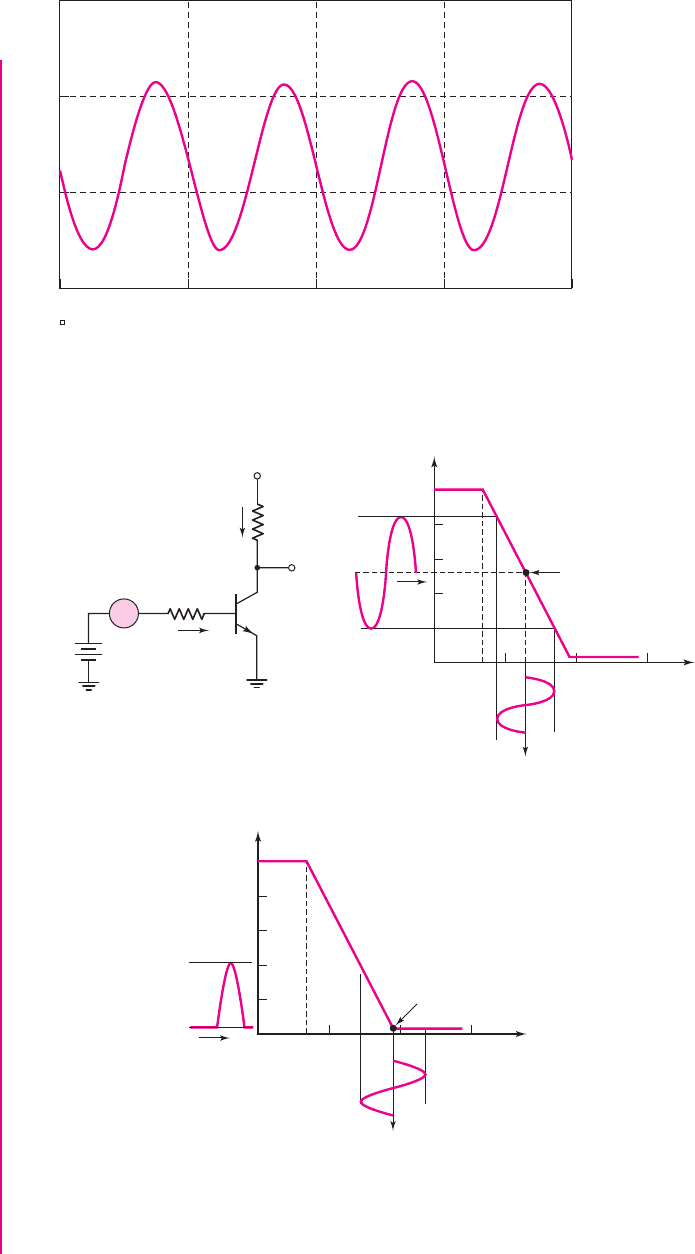
Computer Simulation: A 2 kHz sinusoidal voltage source was placed in the base
circuit of Figure 5.48(a). The amplitude of the time-varying input signal was 0.2 V.
Figure 5.49 shows the output response of the circuit. A sinusoidal signal is superim-
posed on a dc value as we expect. The peak-to-peak output signal is approximately
1.75 V. The time-varying amplification factor is then
|A
v
|=1.75/(2)(0.2) = 4.37
.
This value agrees quite well with the hand analysis.
Comment: As the input voltage changes, we move along the voltage transfer
characteristics as shown in Figure 5.50(b). The negative sign occurs because of the
inverting property of the circuit.
nea80644_ch05_285-368.qxd 06/12/2009 08:42 PM Page 328 F506 Tempwork:Dont' Del Rakesh:June:Rakesh 06-12-09:MHDQ134-05:
1.0V
0s 0.5ms 1.0ms
Time
1.5ms 2.0ms
2.0V
3.0V
4.0V
V (Q1:c)
Figure 5.49 Output signal from the circuit shown in Figure 5.48 for input signals of
V
BB
= 1.3
V and
v
I
= 0.2 sin ωt
(V)
i
B
i
C
+
+
–
–
R
B
= 150 kΩ
R
C
= 5 kΩ
V
BB
= 1.3 V
v
O
Δv
I
Δv
O
Δv
I
V
+
= 5 V
Q-point
Time
Time
v
O
(V)
5
0 123
v
I
(V)
(a)
(c)
v
I
(V)
v
O
(V)
Δv
O
Δv
I
5
0123
Q-point
Time
Time
(b)
Figure 5.50 (a) The inverter circuit with both a dc and an ac input signal; (b) the dc voltage
transfer characteristics, Q-point, and sinusoidal input and output signals; (c) the transfer
characteristics showing improper dc biasing
329
nea80644_ch05_285-368.qxd 06/12/2009 08:42 PM Page 329 F506 Tempwork:Dont' Del Rakesh:June:Rakesh 06-12-09:MHDQ134-05:

330 Part 1 Semiconductor Devices and Basic Applications
Discussion: In this example, we have biased the transistor in the center of the active
region. If the input signal
v
I
is a sinusoidal function as shown in Figure 5.50(b),
then the output signal
v
O
is also a sinusoidal signal, which is the desired response
for an analog circuit. (This assumes the magnitude of the sinusoidal input signal is
not too large.) If the Q-point, or dc biasing, of the transistor were at
v
I
= 1.9
V and
v
O
= 0.2
V, as in Figure 5.50(c), the output response changes. Shown in the figure is
a symmetrical sinusoidal input signal. When the input sinusoidal signal is on its pos-
itive cycle, the transistor remains biased in saturation and the output voltage does not
change. During the negative half of the input signal, the transistor becomes biased in
the active region, so a half sinusoidal output response is produced. The output signal
is obviously not a replication of the input signal.
This discussion emphasizes the importance of properly biasing the transistor for
analog or amplifier applications. The primary objective of this chapter, as stated pre-
viously, is to help readers become familiar with transistor circuits, but it is also to en-
able them to design the dc biasing of transistor circuits that are to be used in analog
applications.
EXERCISE PROBLEM
Ex 5.13: Redesign the inverter amplifier circuit shown in Figure 5.48(a) such that
the voltage amplification is
v
O
/v
I
=−6.5
. Let
R
B
= 80
k
, and assume
β = 120
and
V
BE
(
on
)
= 0.7
V. Determine the
Q
-point values such that the tran-
sistor is biased in the center of the active region. (Ans. For
Q
-point:
v
O
= 2.6
V,
v
I
= 1.069
V,
I
BQ
= 4.61 μ
A;
R
C
= 4.34
k
)
The small-signal linear amplifier analysis and design are the primary objectives of
the next chapter.
Test Your Understanding
TYU 5.14 For the circuit shown in Figure 5.44, assume circuit and transistor para-
meters of
R
B
= 240
,
V
CC
= 12
V,
V
BE
(on) = 0.7
V,
V
CE
(sat) = 0.1
V, and
β = 75
. Assume that the load is a motor with an effective resistance of
R
C
= 5
.
Calculate the currents and voltages in the circuit, and the power dissipated in the
transistor for (a)
v
I
= 0
and (b)
v
I
= 12
V. (Ans. (a)
i
B
= i
C
= 0
,
v
O
= V
CC
=
12 V,
P = 0
; (b)
i
B
= 47.1
mA,
i
C
= 2.38
A,
v
O
= 0.1
V,
P = 0.271
W)
5.4 BIPOLAR TRANSISTOR BIASING
Objective: • Investigate various biasing schemes of bipolar transistor
circuits, including bias-stable biasing and integrated circuit biasing.
As mentioned in the previous section, in order to create a linear amplifier, we must
keep the transistor in the forward-active mode, establish a Q-point near the center of
the load line, and couple the time-varying input signal to the base. The circuit in Fig-
ure 5.47(a) may be impractical for two reasons: (1) the signal source is not connected
nea80644_ch05_285-368.qxd 06/12/2009 08:42 PM Page 330 F506 Tempwork:Dont' Del Rakesh:June:Rakesh 06-12-09:MHDQ134-05:
Chapter 5 The Bipolar Junction Transistor 331
to ground, and (2) there may be situations where we do not want a dc base current
flowing through the signal source. In this section, we will examine several alternative
biasing schemes. These basic biasing circuits illustrate some desirable and some un-
desirable biasing characteristics. More sophisticated biasing circuits that use addi-
tional transistors and that are used in integrated circuits are discussed in Chapter 10.
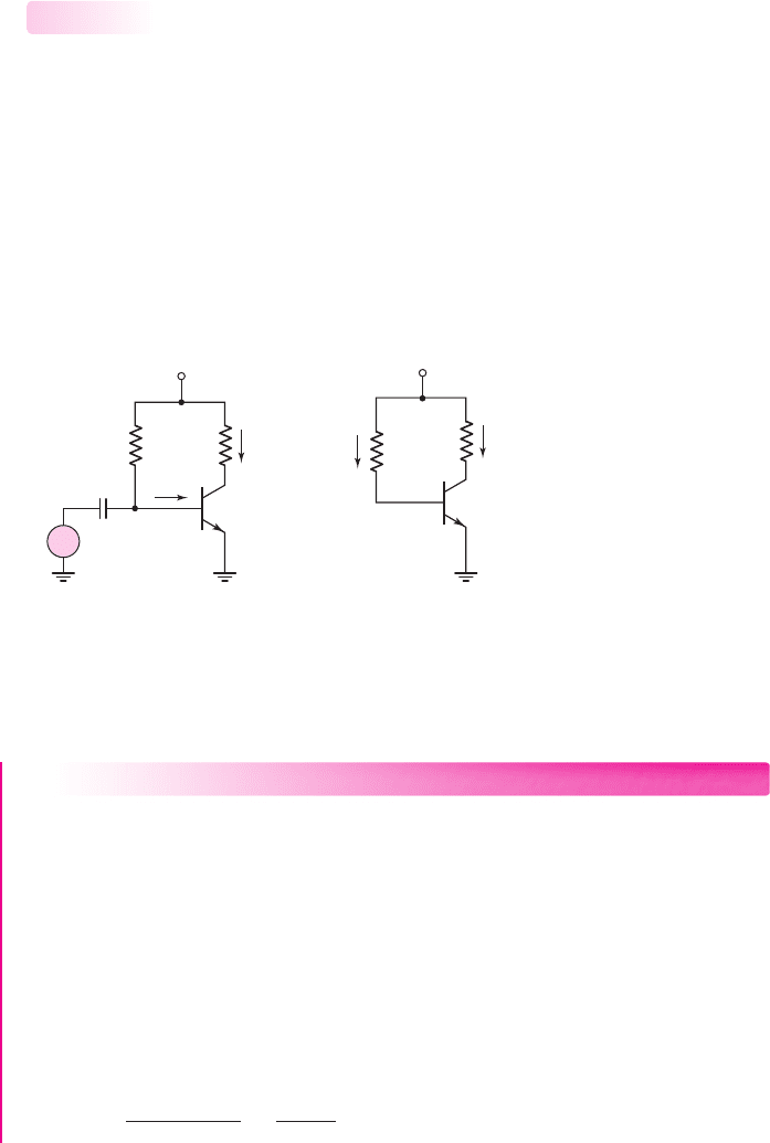
Single Base Resistor Biasing
The circuit shown in Figure 5.51(a) is one of the simplest transistor circuits. There
is a single dc power supply, and the quiescent base current is established through the
resistor
R
B
. The coupling capacitor
C
C
acts as an open circuit to dc, isolating
the signal source from the dc base current. If the frequency of the input signal is large
enough and
C
C
is large enough, the signal can be coupled through
C
C
to the base
with little attenuation. Typical values of
C
C
are generally in the range of 1 to 10
μ
F,
although the actual value depends upon the frequency range of interest (see
Chapter 7). Figure 5.51(b) is the dc equivalent circuit; the Q-point values are indi-
cated by the additional subscript Q.
5.4.1
+
–
v
BE
R
B
R
C
+
–
i
B
i
C
C
C
v
s
V
CC
v
CE
+
–
V
BE
(on)
R
B
R
C
+
–
I
CQ
I
BQ
V
CC
V
CEQ
(a) (b)
+
–
Figure 5.51 (a) Common-emitter circuit with a single bias resistor in the base and (b) dc
equivalent circuit
DESIGN EXAMPLE 5.14
Objective: Design a circuit with a single-base resistor to meet a set of specifications.
Specifications: The circuit configuration to be designed is shown in Figure 5.51(b).
The circuit is to be biased with
V
CC
=+12
V. The transistor quiescent values are to
be
I
CQ
= 1
mA and
V
CEQ
= 6
V.
Choices: The transistor used in the design has nominal values of
β = 100
and
V
BE
(on) = 0.7
V, but the current gain for this type of transistor is assumed to be in
the range
50 ≤ β ≤ 150
because of fairly wide fabrication tolerances. We will as-
sume, in this example, that the designed resistor values are available.
Solution: The collector resistor is found from
R
C
=
V
CC
− V
CEQ
I
CQ
=
12 − 6
1
= 6k
nea80644_ch05_285-368.qxd 06/12/2009 08:42 PM Page 331 F506 Tempwork:Dont' Del Rakesh:June:Rakesh 06-12-09:MHDQ134-05:
332 Part 1 Semiconductor Devices and Basic Applications
The base current is
I
BQ
=
I
CQ
β
=
1mA
100
⇒ 10 μA
and the base resistor is determined to be
R
B
=
V
CC
− V
BE
(on)
I
BQ
=
12 − 0.7
10 μA
= 1.13 M
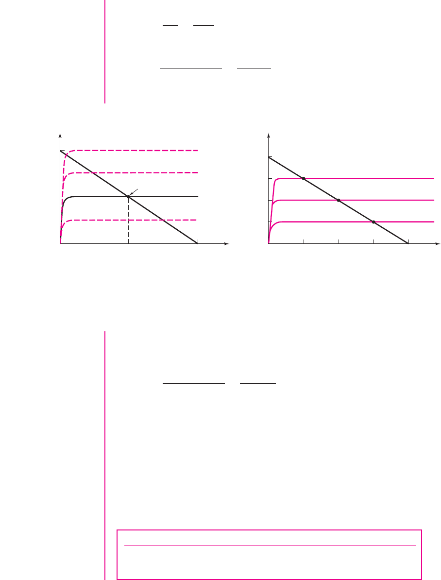
The transistor characteristics, load line, and Q-point for this set of conditions are
shown in Figure 5.52(a).
6012
20
15
5
1
2
v
CE
(V)
i
C
(mA)
Q-point (
b
= 100)
I
BQ
= 10 mA
(a) (b)
2.0
1.5
1.0
0.5
036912
v
CE
(V)
I
C
(mA)
I
B
= 10 mA (b = 150)
I
B
= 10 mA (b = 100)
I
B
= 10 mA (b = 50)
Figure 5.52 (a) Transistor characteristics and load line for the circuit in Figure 5.51 used in
Design Example 5.14; (b) load line and changes in the Q-point for β 50, 100, and 150.
(Note that the base current scale changes compared to the collector current scale.)
Trade-offs:
In this example, we will assume that the resistor values are fixed and will
investigate the effects of the variation in transistor current gain
β
.
The base current is given by
I
BQ
=
V
CC
− V
BE
(on)
R
B
=
12 − 0.7
1.13 M
= 10 μA (unchanged)
The base current for this circuit configuration is independent of the transistor current
gain.
The collector current is
I
CQ
= β I
BQ
and the load line is found from
V
CE
= V
CC
− I
C
R
C
= 12 − I
C
(6)
The load line is fixed. However, the Q-point will change. The transistor Q-point val-
ues for three values of
β
are given as:
β 50 100 150
Q-point values
I
CQ
= 0.50
mA
I
CQ
= 1
mA
I
CQ
= 1.5
mA
V
CEQ
= 9
V
V
CEQ
= 6
V
V
CEQ
= 3
V
nea80644_ch05_285-368.qxd 06/13/2009 05:43 PM Page 332 F506 Hard disk:Desktop Folder:Rakesh:MHDQ134-05:

Chapter 5 The Bipolar Junction Transistor 333
The various Q-points are plotted on the load line shown in Figure 5.52(b). In this fig-
ure, the collector current scale and load line are fixed. The base current scale changes
as
β
changes.
Comment: In this circuit configuration with a single base resistor, the Q-point is not
stabilized against variations in
β
; as
β
changes, the Q-point varies significantly. In
our discussion of the amplifier in Example 5.13 (see Figure 5.50), we noted the
importance of the placement of the Q-point. In the following two examples, we will
analyze and design bias-stable circuits.
Although a value of 1.13 M
for
R
B
will establish the required base current, this
resistance is too large to be used in integrated circuits. The following two examples
will also demonstrate a circuit design to alleviate this problem.
EXERCISE PROBLEM
Ex 5.14: Consider the circuit shown in Figure 5.51(b). Assume
V
CC
= 2.8
V,
β = 150
, and
V
BE
(
on
)
= 0.7
V. Design the circuit such that
I
CQ
= 0.12
mA and
V
CEQ
= 1.4
V. (Ans.
R
C
= 11.7
k
,
R
B
= 2.625
M
)
Test Your Understanding
[Note: In the following exercises, assume the B–E cut-in voltage is 0.7 V. Also
assume the C–E saturation voltage is 0.2 V.]
TYU 5.15 Consider the circuit shown in Figure 5.53. (a) If
β = 120
, determine
R
B
such that
V
CEQ
= 2.5
V. (b) If the current gain varies over the range
80 ≤ β ≤ 160
,
determine the variation in
V
CEQ
. (Ans. (a)
R
B
= 413
k
, (b)
1.67 ≤ V
CEQ
≤ 3.33)
TYU 5.16 For the circuit shown in Figure 5.53, let
R
B
= 800
k
. If the range of
β
is
between 75 and 150, determine a new value of
R
C
such that the Q-point will always
be in the range
1 ≤ V
CEQ
≤ 4
V. What will be the actual range of
V
CEQ
for the new
value of
R
C
? (Ans. For
V
CEQ
= 2.5
V,
R
C
= 4.14
k
; (b)
1.66 ≤ V
CEQ
≤ 3.33
V)
Voltage Divider Biasing and Bias Stability
The circuit in Figure 5.54(a) is a classic example of discrete transistor biasing.
(
IC
biasing is different and will be discussed in Chapter 10.) The single bias resistor
R
B
in the previous circuit is replaced by a pair of resistors
R
1
and
R
2
, and an emitter
resistor
R
E
is added. The ac signal is still coupled to the base of the transistor through
the coupling capacitor
C
C
.
The circuit is most easily analyzed by forming a Thevenin equivalent circuit
for the base circuit. The coupling capacitor acts as an open circuit to dc. The equiva-
lent Thevenin voltage is
V
TH
= [R
2
/(R
1
+ R
2
)]V
CC
and the equivalent Thevenin resistance is
R
TH
= R
1
R
2
5.4.2
R
B
R
C
= 2 kΩ
+5 V
Figure 5.53 Figure for
Exercises TYU 5.15 and
TYU 5.16
nea80644_ch05_285-368.qxd 06/12/2009 08:42 PM Page 333 F506 Tempwork:Dont' Del Rakesh:June:Rakesh 06-12-09:MHDQ134-05:

334 Part 1 Semiconductor Devices and Basic Applications
where the symbol
indicates the parallel combination of resistors. Figure 5.54(b)
shows the equivalent dc circuit. As we can see, this circuit is similar to those we have
previously considered.
Applying Kirchhoff’s law around the B–E loop, we obtain
V
TH
= I
BQ
R
TH
+ V
BE
(on) + I
EQ
R
E
(5.37)
If the transistor is biased in the forward-active mode, then
I
EQ
= (1 +β)I
BQ
and the base current, from Equation (5.37), is
I
BQ
=
V
TH
− V
BE
(on)
R
TH
+(1 +β)R
E
(5.38)
The collector current is then
I
CQ
= β I
BQ
=
β(V
TH
− V
BE
(on))
R
TH
+(1 +β)R
E
(5.39)
EXAMPLE 5.15
Objective: Analyze a circuit using a voltage divider bias circuit, and determine the
change in the Q-point with a variation in
β
when the circuit contains an emitter
resistor.
For the circuit given in Figure 5.54(a), let
R
1
= 56
k
,
R
2
= 12.2
k
,
R
C
=
2k
,
R
E
= 0.4
k
,
V
CC
= 10
V,
V
BE
(on) = 0.7
V, and
β = 100
.
Solution: Using the Thevenin equivalent circuit in Figure 5.54(b), we have
R
TH
= R
1
R
2
= 5612.2 = 10.0k
and
V
TH
=
R
2
R
1
+ R
2
· V
CC
=
12.2
56 + 12.2
(10) = 1.79 V
C
C
R
C
R
E
v
s
R
2
R
1
+
–
I
CQ
V
CC
V
CEQ
+
–
V
TH
R
TH
R
E
+
–
I
BQ
I
EQ
R
C
I
CQ
V
CC
V
CEQ
(a) (b)
+
–
Figure 5.54 (a) A common-emitter circuit with an emitter resistor and voltage divider bias
circuit in the base; (b) the dc circuit with a Thevenin equivalent base circuit
nea80644_ch05_285-368.qxd 06/12/2009 08:42 PM Page 334 F506 Tempwork:Dont' Del Rakesh:June:Rakesh 06-12-09:MHDQ134-05:

Chapter 5 The Bipolar Junction Transistor 335
Writing the Kirchhoff voltage law equation around the B–E loop, we obtain
I
BQ
=
V
TH
− V
BE
(on)
R
TH
+(1 +β)R
E
=
1.79 − 0.7
10 + (101)(0.4)
⇒ 21.6 μA
The collector current is
I
CQ
= β I
BQ
= (100)(21.6 μA) ⇒ 2.16 mA
and the emitter current is
I
EQ
= (1 +β)I
BQ
= (101)(21.6 μA) ⇒ 2.18 mA
The quiescent C–E voltage is then
V
CEQ
= V
CC
− I
CQ
R
C
− I
EQ
R
E
= 10 −(2.16)(2) −(2.18)(0.4) = 4.81 V
These results show that the transistor is biased in the active region.
If the current gain of the transistor were to decrease to
β = 50
or increase to
β = 150
, we obtain the following results:
The load line and Q-points are plotted in Figure 5.55. The variation in Q-points for
this circuit configuration is to be compared with the variation in Q-point values
shown previously in Figure 5.52(b).
For a 3 : 1 ratio in
β
, the collector current and collector–emitter voltage change
by only a 1.29 : 1 ratio.
Comment: The voltage divider circuit of
R
1
and
R
2
can bias the transistor in its ac-
tive region using resistor values in the low kilohm range. In contrast, single resistor
biasing requires a resistor in the megohm range. In addition, the change in
I
CQ
and
V
CEQ
with a change in
β
has been substantially reduced compared to the change
shown in Figure 5.52(b). Including an emitter resistor
R
E
has tended to stabilize the
Q-point. This means that including the emitter resistor helps to stabilize the Q-point
with respect to variations in
β
. Including the resistor
R
E
introduces negative feed-
back, as we will see in Chapter 12. Negative feedback tends to stabilize circuits.
β 50 100 150
I
BQ
= 35.9 μ
A
I
BQ
= 21.6 μ
A
I
BQ
= 15.5 μ
A
Q-point values
I
CQ
= 1.80
mA
I
CQ
= 2.16
mA
I
CQ
= 2.32
mA
V
CEQ
= 5.67
V
V
CEQ
= 4.81
V
V
CEQ
= 4.40
V
4.0
3.0
2.0
1.0
0 246810
I
C
(mA)
V
CE
(V)
b = 150
b = 100
b = 50
Figure 5.55 Load lines and Q-point values for Example 5.15
nea80644_ch05_285-368.qxd 06/12/2009 08:42 PM Page 335 F506 Tempwork:Dont' Del Rakesh:June:Rakesh 06-12-09:MHDQ134-05:

336 Part 1 Semiconductor Devices and Basic Applications
EXERCISE PROBLEM
Ex 5.15: For the circuit shown in Figure 5.54(a), let
V
CC
= 3.3
V,
R
E
= 500
,
R
C
= 4
k
,
R
1
= 85
k
,
R
2
= 35
k
, and
β = 150
. (a) Determine
R
TH
and
V
TH
.
(b) Find
I
BQ
,
I
CQ
, and
V
CEQ
. (c) Repeat part (b) for
β = 75
. (Ans. (a)
R
TH
=
24.8
k
,
V
TH
= 0.9625
V; (b)
I
BQ
= 2.62 μ
A,
I
CQ
= 0.393
mA,
V
CEQ
= 1.53
V;
(c)
I
BQ
= 4.18 μ
A,
I
CQ
= 0.314
mA,
V
CEQ
= 1.89
V)
Considering Equation (5.39), the design requirement for bias stability is
R
TH
(1 +β)R
E
. Consequently, the collector current is approximately
I
CQ
∼
=
β(V
TH
− V
BE
(on))
(1 + β)R
E
(5.40)
Normally,
β 1
; therefore,
β/(1 + β)
∼
=
1
, and
I
CQ
∼
=
(V
TH
− V
BE
(on))
R
E
(5.41)
Now the quiescent collector current is essentially a function of only the dc volt-
ages and the emitter resistance, and the Q-point is stabilized against
β
variations.
However, if
R
TH
is too small, then
R
1
and
R
2
are small, and excessive power is dis-
sipated in these resistors. The general rule is that a circuit is considered bias stable
when
R
TH
∼
=
0.1(1 + β)R
E
(5.42)
DESIGN EXAMPLE 5.16
Objective: Design a bias-stable circuit to meet a set of specifications.
Specifications: The circuit configuration to be designed is shown in Figure 5.54(a).
Let
V
CC
= 5
V and
R
C
= 1
k
. Choose
R
E
and determine the bias resistors
R
1
and
R
2
such that the circuit is considered bias stable and that
V
CEQ
= 3
V.
Choices: Assume the transistor has nominal values of
β = 120
and
V
BE
(on) =
0.7 V. We will choose standard resistor values and will assume that the transistor cur-
rent gain varies over the range
60 ≤ β ≤ 180
.
Design Pointer: Typically, the voltage across
R
E
should be on the same order of
magnitude as
V
BE
(on). Larger voltage drops may mean the supply voltage
V
CC
has
to be increased in order to obtain the required voltage across the collector-emitter and
across
R
C
.
Solution: With
β = 120
,
I
CQ
≈ I
EQ
. Then, choosing a standard value of 0.51 k
for
R
E
, we find
I
CQ
∼
=
V
CC
− V
CEQ
R
C
+ R
E
=
5 − 3
1 + 0.51
= 1.32 mA
The voltage drop across
R
E
is now (1.32)(0.51) = 0.673 V, which is approximately
the desired value. The base current is found to be
I
BQ
=
I
CQ
β
=
1.32
120
⇒ 11.0 μA
nea80644_ch05_285-368.qxd 06/12/2009 08:42 PM Page 336 F506 Tempwork:Dont' Del Rakesh:June:Rakesh 06-12-09:MHDQ134-05:

Chapter 5 The Bipolar Junction Transistor 337
Using the Thevenin equivalent circuit in Figure 5.54(b), we find
I
BQ
=
V
TH
− V
BE
(on)
R
TH
+(1 +β)R
E
For a bias-stable circuit,
R
TH
= 0.1(1 +β)R
E
,or
R
TH
= (0.1)(121)(0.51) = 6.17 k
Then,
I
BQ
= 11.0 μA ⇒
V
TH
−0.7
6.17 + (121)(0.51)
which yields
V
TH
= 0.747 +0.70 = 1.447 V
Now
V
TH
=
R
2
R
1
+ R
2
V
CC
=
R
2
R
1
+ R
2
(5) = 1.447 V
or
R
2
R
1
+ R
2
=
1.447
5
= 0.2894
Also,
R
TH
=
R
1
R
2
R
1
+ R
2
= 6.17 k = R
1
R
2
R
1
+ R
2
= R
1
(0.2894)
which yields
R
1
= 21.3k
and
R
2
= 8.69 k
From Appendix C, we can choose standard resistor values of
R
1
= 20
k
and
R
2
= 8.2
k
.
Trade-offs: We will neglect, in this example, the tolerance effects of the resistors
(end-of-chapter problems such as Problems 5.18 and 5.40 do include tolerance ef-
fects). We will consider the effect on the transistor Q-point values of the common-
emitter current gain variation.
Using the standard resistor values, we have
R
TH
= R
1
R
2
= 208.2 = 5.82 k
and
V
TH
=
R
2
R
1
+ R
2
(V
CC
) =
8.2
20 + 8.2
(5) = 1.454 V
The base current is given by
I
BQ
=
V
TH
− V
BE
(on)
R
TH
+(1 +β)R
E
nea80644_ch05_285-368.qxd 06/12/2009 08:42 PM Page 337 F506 Tempwork:Dont' Del Rakesh:June:Rakesh 06-12-09:MHDQ134-05: