Zuo-Guang. Ye Advanced Dielectric Piezoelectric and Ferroelectric Materials: Synthesis, Characterisation and Applications
Подождите немного. Документ загружается.

Handbook of dielectric, piezoelectric and ferroelectric materials610
with respect to the island distribution (particularly the spacing between the
self-patterning structures should be taken into account). The mechanical
imprint technique seems to be very attractive due to its efficient (cheap and
fast) way of application on a large-area scale.
20.3 Physical properties of the nano-islands
20.3.1 Structural investigation
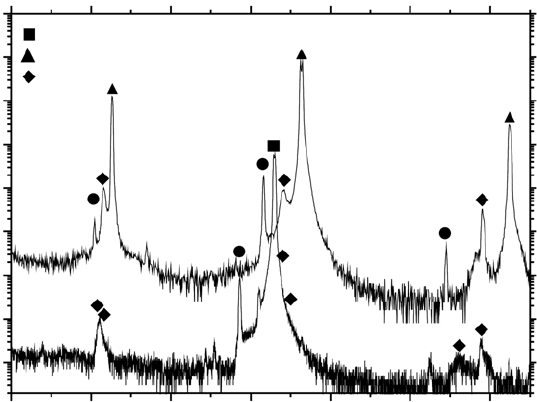
For larger and smaller structures X-ray diffraction (XRD) analysis and/or
high-resolution transmission electron microscopy (HRTEM), respectively,
were performed to obtain structural information on the nanocrystals. XRD
diffraction patterns of PZT/STO nano-islands, obtained at 800 °C, show the
00l reflections from the STO substrate (cubic), and only the 00l reflections
of the tetragonal PZT (Fig. 20.9). This proves the epitaxial relationship
between the substrate and the nanostructures. No secondary phase peaks
were detected in the XRD patterns, confirming the formation of a good-
quality perovskite phase. XRD has shown that the PZT islands on STO have
a c-axis orientation. The XRD patterns obtained for PZT nano-islands grown
on (001) MgO substrate showed more diffraction peaks that could be indexed
as (h00) and (00l) reflections (Fig. 20.9). Obviously the larger lattice misfit
Intensity [a.u.]
MgO
STD
PZT
001
001
001
001
001
002
002
002
200
003
003
003
003
10 20 30 40 50 60 70
2θ [degrees]
20.9
X-ray diffraction pattern of PZT 52/48 nanocrystals on (001) STO
and (001) MgO substrates. The peaks labelled with circles indicate
substrate peaks originating from the remaining Cu K
β
radiation.
WPNL2204
Nanosized ferroelectric crystals 611
(PZT/MgO) results in the formation of epitaxial islands with both a- and c-
axis orientations.
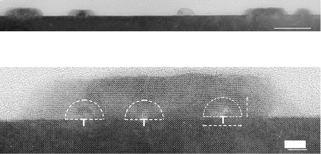
Further structural information about the nanoislands was obtained from
TEM analysis (Figs 20.10 and 20.11). The low-magnification pictures (Fig.
20.10) show that all islands have a uniform height. Moreover, all the structures
have a well-defined truncated pyramidal shape with relatively sharp facets.
The facets preferably consist of {111} or {110} planes as the side walls of
the nanocrystals. The top facet of the island is parallel to the {001} substrate
plane. The appearance of such facets is related to previous research that
showed the ultra-thin film breaking up into small structures with lower energy
planes as result of microstructural instability and that in such a way the total
energy is reduced [12–14].
The HRTEM images of several PZT 52/48 /STO nano-islands have
confirmed that they are single crystals which are uniformly c-domain-oriented
without any 90° domains being present. All nano-islands have almost an
atomically flat surface. The rare steps observed on the top facet are related
to the substrate steps with a height of half a unit cell. The interface is
atomically flat, which indicates that any diffusion between the nanocrystal
and the substrate does not occur. The crystals are free from volume defects,
and the only defects are dislocations concentrated along the interface. They
are caused by stress relaxation-induced by the lattice mismatch between the
STO substrate and the PZT islands. The distance d between the dislocations
estimated on the basis of several tens of nano-islands gives values between
9 and 13 nm. This value is in agreement with the calculated spacing, d = a/
δ (where a is the lattice constant and δ is the value of the lattice misfit),
which is about 12 nm. It should be underlined that in each island there is a
50 nm
STO
PZT
~8 nm
~4 nm
4 nm
[010]
20.10
Low-magnification electron micrograph of PZT 52/48 on STO.
20.11
Cross-section HRTEM image of a single PZT 52/48 nanocrystal.
The distorted regions near misfit dislocations (showed by ‘T’) are
marked by dotted line.
WPNL2204
Handbook of dielectric, piezoelectric and ferroelectric materials612
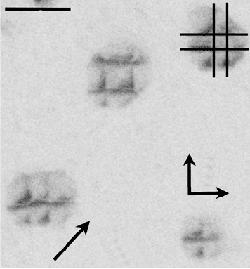
60 nm
g
= [220]
[010]
[100]
20.12
Plan-view HRTEM image of PZT 52/48 nano-islands on STO
substrate (the dislocation network is marked in the upper right
corner).
network of misfit dislocations present, the dislocations on average having a
mutual distance of 12 nm. The dislocation network is clearly visible on plan-
view TEM images (see Fig. 20.12).
20.3.2 The growth mechanism of the nano-islands
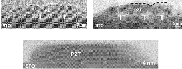
To investigate the growth mechanism of the PZT 52/48 nano-islands several
samples were prepared under different conditions: the crystallization
temperature was varied between 650 and 800 °C and the annealing time
between 5 min and 10 h. All experiments were carried out on samples with
the same thickness of the initial layer. Each sample was studied using HRTEM
(Fig. 20.13). In the early stage of nucleation the pre-existing holes penetrate
down to the substrate surface. As a result a non-faceted discontinuous layer
of about 3–4 nm thickness is formed. During longer heat treatments (650 °C
for 1 h) the nano-islands migrate on the substrate surface and coalesce into
larger irregular structures. The nanostructures crystallized at higher
temperatures (e.g. at 800 °C for 5 min) have a better thickness uniformity;
however, the coalescence process is not finished. An annealing as long as
1 h at 800 °C is required to form the equilibrium shape and distribution of the
islands. A thermal treatment at 800 °C longer than 1 h does not lead to significant
changes in island morphology, shape and distribution.
As it was previously shown, the nanostructure formation is connected
with the lowering of the interfacial energy [12–14]. In order to minimize the
WPNL2204
Nanosized ferroelectric crystals 613
PZT/STO interfacial energy, pre-existing ‘holes’ at the thin, amorphous CSD-
prepared PZT layer accumulate during annealing and then grow through the
PZT layer to uncover the STO substrate, leading to isolated islands with
misfit dislocations at the interface. At longer annealing times at high
temperatures, isolated PZT islands may coalesce into bigger ones,
simultaneously forming energetically favorable {111} and {110} facets.
However, a certain amount of thermal energy (equivalent to the 1 h treatment
at 800 °C) is required to reach the equilibrium state in which well-defined
facets appear.
20.3.3 Ferroelectric properties
Owing to the small size of the nanocrystals, their characterization cannot be
achieved using conventional measurement techniques. For this purpose,
scanning probe techniques, in particular piezoresponse force microscopy
(PFM), have proven to be most valuable. The local polarization state and the
electromechanical properties of the ferroelectric nanostructures can be probed
via the converse piezoelectric effect using the AFM technique combined
with a lock-in technique. This method is based on the detection of local
vibrations of a ferroelectric sample induced by a testing a signal applied
between the conductive tip of the PFM and the bottom electrode of the
sample [7, 23]. The role of the bottom electrode is usually played by a
conductive substrate; in the case of PZT nano-islands Nb-doped STO substrates
allowed to study the ferroelectric properties. Because of the strong relation
between the piezoelectric coefficient and the spontaneous polarization the
material expands or contracts under the applied electric field. The sign of the
piezoelectric coefficient is determined by the direction of the spontaneous
polarization with respect to that of the applied electric field.
(a) (b)
(c)
20.13
Cross-sectional HRTEM micrographs of PZT nano-islands
grown on STO substrates (a) at 650 °C for 1 h, (b) at 800 °C for 5 min
and (c) at 800 °C for 1 h. The dashed lines in (a) and (b) show the
coalescence of two neighboring islands.
WPNL2204
Handbook of dielectric, piezoelectric and ferroelectric materials614
The PZT 52/48/STO:Nb islands with heights above 25 nm or with a large
lateral size show a well-developed piezoelectric hysteresis loop. Figure 20.14
shows the topography and piezoresponse images proving the switching of
the polarization in crystals with a height of 15 nm. The grain marked by the
dashed contour was successively polarized negatively (polarization pointing
into the sample, Fig. 20.14b), and then positively (Fig. 20.14c) by the biased
AFM tip. It was also possible to record a loop on an island of irregular shape.
Similar loops were obtained for islands with heights above 25 nm and smaller
lateral size and for the structures after mechanical imprint. For smaller structures
(smaller island volume, e.g. low height and low lateral size) there were
problems in obtaining a hysteresis loop.
20.3.4 Impact of the misfit dislocations on the
ferroelectric switching
In order for switching to occur it is necessary that the crystal possesses more
than a critical number of unit cells with the proper crystallographic structure.
The PZT/STO nano-islands have relatively large regions affected by the
dislocation network (see Figs 20.11 and 20.12). In order to investigate the
long-range strain fields associated with the dislocation, a geometric phase
Signal (a.u.)
Bias (V)
–30 –20 –10 0 10 20 30
(d)
500 nm
(a)
(b) (c)
20.14
Switching of an individual nanocrystal by PFM: (a) topography
(
z
-scale 25nm) and piezoresponse images after applying (b) a
negative and (c) a positive dc voltage. (d) Hysteresis loop recorded
on the structure in the middle of the image (a).
WPNL2204
Nanosized ferroelectric crystals 615
analysis of HRTEM images was performed. Based on this analysis, the
details of which are given in Chu et al. [24], the in-plane (ε
xx
), shear (ε
xy
) and
out-of-plane (ε
yy
) strain fields have been determined. The strain, associated
with the misfit dislocations, is predominantly localized on the PZT side. The
estimation has shown that the strain extends into the PZT phase for about 4
nm from the dislocation core (Fig. 20.15). Based on this value it is possible
to calculate the partial volume (V
p
) affected by the dislocations. In the case
of PZT 52/48 nano-islands on STO, with a base length of about 50 nm and
a height of about 9 nm, V
p
can be estimated to about 50% of the total volume
of the island. Because ferroelectricity is a cooperative phenomenon of a
sufficiently large number of non-centrosymmetric unit cells, this significant
value could influence the ferroelectric properties. In the affected regions, the
PZT lattice deviates from the regular tetragonal structure, and the long-range
correlations of the local polarization may thus break down, leading to a
polarization instability. As a result, ferroelectric switching was not observed
in these nano-islands using PFM. By contrast, in PZT 52/48 islands with a
double height of ~20 nm, V
p
is only about 25% and in this case a well-
defined piezoresponse loop has been recorded (see Fig. 20.14).
To distinguish the impact of a purely intrinsic size effect (which in principle
may occur in structures with a height of only about 10 nm) from the influence
of dislocations, dislocation-free islands were fabricated and investigated.
20.15
Cross-sectional HRTEM image of a PZT nano-island with the
distorted regions near misfit dislocations (dashed line). The
additional half-plane on the substrate side is marked as a solid line.
WPNL2204
Handbook of dielectric, piezoelectric and ferroelectric materials616
One of such systems is PT/STO, where the calculated spacing between misfit
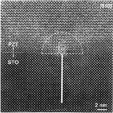
dislocations (about 195 nm) is much larger than the island size. HRTEM
studies have proven that the PT/STO interface is atomically sharp and misfit
dislocations are not present (see Fig. 20.16). An individual PT island on STO
has shown a piezoelectric hysteresis loop, proving the switching behavior of
10 nm high PT structures (Fig. 20.17). This result is also in good agreement
with recent results showing the ferroelectric properties of thin lead titanate
film with thickness of several unit cells [25, 26].
20.3.5 Dislocations and domain wall formation
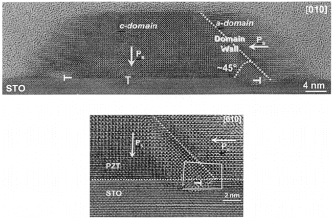
During the analysis of nanoislands with different interfacial strain, a few
islands were found that contain a twin boundary [27]. The HREM image of
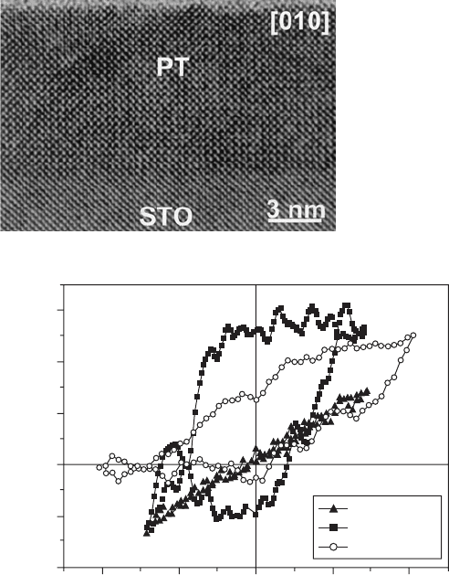
PZT ~ 10 nm
PZT ~ 20 nm
PT ~ 9 nm
Applied bias (V)
–10 –5 0 5 10
PFM signal (a.u.)
–100
–50
0
50
100
150
20.17
PFM measurements of local hysteresis loop of three different
islands.
20.16
HRTEM image of PT nanocrystal on STO.
WPNL2204
Nanosized ferroelectric crystals 617
such an island is shown in Fig. 20.18. This island is slightly larger than those
discussed before. The PZT 40/60 island shows an epitaxial c-axis orientation
with respect to the substrate; however, a small region (on the top right on
Fig. 20.18) possesses an a-axis orientation. Between these two regions a
90 °C domain wall is observed. The estimated angular separation (α) between
these two regions is about 1°
which is smaller than the calculated value of 2°.
This suggests that the ferroelastic strain distribution near the domain wall is
rather complex. The defect analysis has shown that – besides the dislocations
related to the relaxation of the lattice mismatch (with an extra half plane on
the substrate side) – there is a dislocation related to another extra half plane
in the substrate which is parallel to the interface, i.e. a dislocation with a
Burger’s vector perpendicular to the plane of the interface.
The geometric phase analysis of HRTEM images was used in order to
determine the strain near the domain wall. The corresponding details were
published in Chu et al. [27]. In the region far from the interface the strain
distorts both the a- and c-domain regions. The wall region exhibits a
compressively strained area embedded in a relatively strain-free surrounding.
The estimated thickness of the domain wall, based on this analysis, is about
1.5 nm (close to four unit cells). A more complicated situation prevails near
the interface. The 90° domain wall does not end directly on the edge dislocation,
but on a distance of about 2 nm from it. The strain distribution in this region
20.18
Cross-sectional HRTEM image of a PZT 40/60 island showing
the twin wall. Bottom: Magnified section of the region close to the
interfacial dislocation.
WPNL2204
Handbook of dielectric, piezoelectric and ferroelectric materials618
is more complicated. Near the edge dislocation with a perpendicular Burger’s
vector a tensile strain is observed. Near the interface and the wall, this
tensile strain is reduced by the compressive strain caused by the presence of
the twin wall. This elastic coupling by partial strain annihilation qualitatively
minimizes the long-range electromechanical energy. The slight deviation
between the calculated and the observed value of the angular separation and
the gentle broadening of the wall width near the dislocation core can be
understood as effects of the interaction of long-range strain fields of the twin
wall and the dislocation core. More important for future PZT applications is
the fact that the switching behavior of the islands containing a twin wall is
different. If an electric field is applied perpendicularly to the interface of the
island, switching of the single c-domain state has to be accomplished by
removing the twin wall from the island. This electric field-driven movement
is, however, difficult, since the long-range strain field of the interfacial
dislocation imposes a potential barrier on the twin wall. This fact can cause
difficulties in mobilizing the twin wall by applying electric fields. As a
consequence, the twin wall in the islands should thus not be electrically
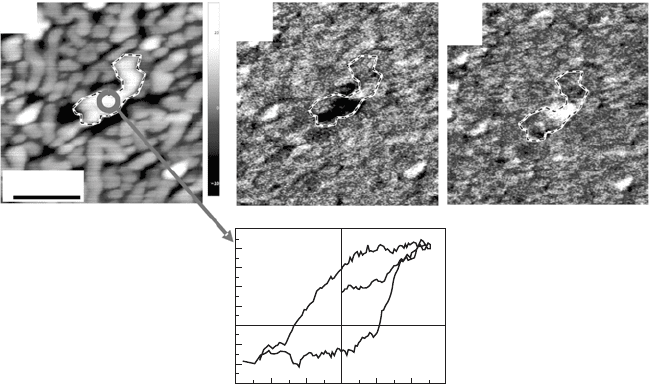
active. Indeed the nano-islands, investigated by PFM, show large regions
where the PFM signal is about zero (see Fig. 20.19a). This value suggests the
presence of the 90° domains. Figure 20.19(b) shows the hysteresis loop
acquired on the structure in the middle of the image. Its shape reveals the
huge imprint, which can be associated also with the domain pinning.
20.4 Conclusions and future trends
The self-patterning method is a new appealing way of nano-island fabrication.
The lateral size and the height of the nanostructures can be controlled by
adjustments of the deposited film thickness, of the crystallization conditions
and a proper choice of the substrate. The dislocations present in such structures
can have a large impact on the final properties. The network of misfit
dislocations forming as a result of lattice mismatch relaxation affects a relatively
large volume of the island. Such islands are not switchable and they lose the
useful properties for an application as memories or storage devices. Dislocations
with a Burger’s vector perpendicular to the interface and connected with a
twin wall can render the system electrically inactive. Thus the formation of
such defects has to be avoided, if ferroelectric oxides with nanometer-size
sizes are to be employed for future applications that require ferroelectric
switching.
It appears that an ‘interface engineering’ is required for epitaxial nano-
islands, if the latter should retain their ferroelectric properties, in particular
polarization switchability. The substrate should be carefully chosen, not only
under the aspect of chemical stability (avoiding interfacial diffusion and
reaction processes at the processing temperatures), but also adapting the
WPNL2204
Nanosized ferroelectric crystals 619
(a)
20.19
(a) AFM image of PZT 40/60 nano-islands on STO (200 × 200
nm
2
,
z
range 10 nm). The marked regions have shown a PFM signal
about zero. (b) Hysteresis loop recorded on the structure in the
middle of the image (a).
Applied bias (V)
(b)
–2–4 0 2 4
–30
–40
–20
–10
0
10
20
30
40
d
zz
(pm/V)
WPNL2204