Zuo-Guang. Ye Advanced Dielectric Piezoelectric and Ferroelectric Materials: Synthesis, Characterisation and Applications
Подождите немного. Документ загружается.

Handbook of dielectric, piezoelectric and ferroelectric materials620
crystal structure and lattice parameter of the substrate to those of the ferroelectric
nano-islands, in this way minimizing the density of interfacial dislocations
and other interfacial defects at the nanostructure/substrate interface. Nanosized
ferroelectric crystals are thus another area of technology where interface
engineering is indispensable.
20.5 Acknowledgments
This work has been performed in close collaboration with M.-W. Chu, M.
Dawber, C. Harnagea, R. Scholz and J.F. Scott, to whom the authors are
grateful for their respective contributions. Special thanks are due to U. Gösele
for his continuous support.
20.6 References
1. Scott J F, Ferroelectric Memories, Berlin, Springer, 2000.
2. International FRAM roadmap; http://public.itrs.net.
3. Wang Y G, Zhong W L and Zhang P L, ‘Surface and size effects on ferroelectric
films with domain structures’, Phys Rev B, 1995 51 5311.
4. Waser R (ed.), Nanoelectronics and Information Technology: Advanced Electronic
Materials and Novel Devices, Weinheim, Wiley-VCH, 2003.
5. Ganpule C S, Stanishevsky A, Su Q, Aggarwal S, Melngailis J, Williams E and
Ramesh R, ‘Scaling of ferroelectric properties in thin films’, Appl Phys Lett, 1999
75 409.
6. Harnagea C, Alexe M, Schilling J, Choi J, Wehrspohn R B, Hesse D and Gösele U,
‘Mesoscopic ferroelectric cell arrays prepared by imprint lithography’, Appl Phys
Lett, 2003 83 1827.
7. Alexe M, Harnagea, C and Hesse D, ‘Non-conventional micro- and nanopatterning
techniques for electroceramics’, J Electroceramics, 2004 12 69.
8. Alexe M, Harnagea C, Hesse D and Gösele U, ‘Patterning and switching of nanosize
ferroelectric memory cells’, Appl Phys Lett, 1999 75 1793.
9. Fujisawa H, Shimizu M, Niu H, Honda K and Ohtani S, ‘Observations of domain
structure at initial growth stage of PbTiO
3
thin films growth by MOCVD’, Mat Res
Soc Symp Proc, 2000 596 321.
10. Fujisawa F, Morimoto K, Shimizu M, Niu H, Honda K and Ohtani S, ‘Piezoresponse
measurements of Pb(Zr,Ti)O
3
island structure using scanning probe microscopy’,
Mat Res Soc Symp Proc, 2001 655 CC10.4.1.
11. Alexe M, Harnagea C, Visinoiu A, Pignolet A, Hesse D and Gösele U, ‘Patterning
and switching of nano-size ferroelectric memory cells’, Scripta Materialia, 2001 44
1175.
12. Seifert A, Vojta A, Speck J S and Lange F F, ‘Microstructural instability in single-
crystal thin films’, J Mater Res, 1996 11 1470.
13. Zhao L, Chien A T, Lange F F and Speck J S, ‘Microstructural development of
BaTiO
3
powders synthesized by aqueous methods’, J Mater Res, 1996 11 1325.
14. Lee W T, Salje E K H and Dove M T, ‘Effect of surface relaxations on the equilibrium
growth morphology of crystals: platelet formation’, J Phys: Condens Matter, 1999
11 7385.
WPNL2204
Nanosized ferroelectric crystals 621
15. Waser R, Schneller T, Hoffmann-Eifert S and Ehrhart P, ‘Advanced chemical deposition
techniques – from research to production’, Integr Ferroelectr, 2001 36 3.
16. Roelofs A, Schneller T, Szot K and Waser R, ‘Piezoresponse force microscopy of
lead titanate nanograins possibly reaching the limit of ferroelectricity’, Appl Phys
Lett, 2002 81 5231.
17. Roelofs A, Schneller T, Szot K and Waser R, ‘Towards the limit of ferroelectric
nanosized grains’, Nanotechnology, 2003 14 250.
18. Harnagea C, Pignolet A, Alexe M and Hesse D, ‘Piezoresponse scanning force
microscopy: what quantitative information can we really get out of piezoresponse
measurements on ferroelectric thin films? Integr Ferroelectr, 2002 44 113.
19. Szafraniak I, Harnagea C, Scholz R, Bhattacharyya S, Hesse D and Alexe M,
‘Ferroelectric epitaxial nanocrystals obtained by a self-patterning method’, Appl
Phys Lett, 2003 83 2211.
20. Shchukin V A and Bimberg D, ‘Spontaneous ordering of nanostructures on crystal
surfaces’, Rev Mod Phys, 1999 71 1125.
21. Williams R S, Medeiros-Ribeiro G, Kamins T I and Ohlberg D A A, ‘Thermodynamics
of the size and shape of nanocrystals: epitaxial Ge on Si(001)’, Annu Rev Phys
Chem, 2000 51 527.
22. Dawber M, Szafraniak I, Alexe M and Scott J F, ‘Self patterning of arrays of ferroelectric
capacitors: description by theory of substrate mediated strain interactions’, J Phys:
Condens Matter, 2003 15 L667.
23. Alexe M and Gruverman A (eds.), Nanoscale Characterisation of Ferroelectric
Materials – Scanning Probe Microscopy Approach, Berlin, Springer, 2004.
24. Chu M-W, Szafraniak I, Harnagea C, Scholz R, Hesse D, Alexe M and Gösele U,
‘Impact of misfit dislocations on polarization instability of epitaxial nanostructured
ferroelectric perovskites’, Nature Materials, 2004 3 87.
25. Streiffer S K, Eastman J A, Fong D D, Thompson C, Munkholm A, Ramana Murty
M V, Auciello O, Bai G R and Stephenson G B, ‘Observation of nanoscale 180°
stripe domains in ferroelectric PbTiO
3
thin films’, Phys Rev Lett, 2002 89 067601.
26. Fong D D, Stephenson G B, Streiffer S K, Eastman J A, Auciello O, Fuoss P H and
Thompson C, ‘Ferroelectricity in ultrathin perovskite films’, Science, 2004 304
1650.
27. Chu M-W, Szafraniak I, Hesse D, Alexe M and Gösele U, ‘Elastic coupling between
90° twin walls and interfacial dislocations in epitaxial ferroelectric perovskites’,
Phys Rev B, 2005 72 174112.
WPNL2204

622
21.1 Introduction
In recent decades, domain engineering has become one of the most important
areas of ferroelectric science and technology. The main target of domain
engineering is the manufacturing of stable tailored domain patterns in
commercially available ferroelectrics possessing characteristics important
for applications. The ability to introduce the spatial modulation of the electro-
optic, photorefractive, piezoelectric, and nonlinear optical properties by the
creation of periodic domain structure opens wide possibilities in the
manufacturing of devices with upgraded performance. The relatively low
price of these devices can be achieved under mass production using lithographic
electrode patterning for periodical poling. The potential for this technology
is ready to expand into a wider market.
The optimization of the poling process resulting from the fundamental
studies of the domain kinetics is expected to enable the fabrication of sub-
micrometer-pitch gratings and engineered 1D and 2D structures, which could
meet the demanding specifications for the photonic applications. The ultimate
interest is the exploitation of fine (nanoscale) domain structures with capabilities
for optical devices. It is necessary to keep in mind that for achieving high
conversion efficiency the structure has to be precisely reproducible with the
period dispersion about 10nm.
The idea to optimize the ferroelectric properties by the creation of stable
tailored domain structures was advanced 30 years ago by Newnham, Cross
and coworkers (Newnham et al., 1975), who discussed the ability to modify
the crystal properties for piezoelectric devices by producing ‘domains which
are not to be switched during device operation.’ In parallel the independent
branch of the domain engineering aimed at creating the periodically poled
nonlinear optical crystals for light frequency conversion and production of
quasi-phase-matched devices has been developed. The original method of
phase-matching by reversing the sign of the nonlinear coefficient every
coherence length, when a phase difference over π is accumulated between
21
Nano- and micro-domain engineering in
normal and relaxor ferroelectrics
V Y S H U R, Ural State University, Russia
WPNL2204
Nano- and micro-domain engineering 623
the interacting waves, was proposed by Armstrong et al. (1962) and was
applied experimentally to an array of ferroelectric domains by Miller (1964).
The LiNbO
3
(LN) and LiTaO
3
(LT) single crystals are the most popular
materials because of their record electro-optic and nonlinear optical properties.
LN and LT are favorable for the production of precise periodic domain
structures, because 180° domain walls in both crystals are strictly oriented in
proper crystallographic directions.
Feng et al. (1980) and Ming et al. (1982) were the first to produce
periodically poled LN (PPLN) by growing doped LN crystals in periodically
variable electric field conditions, giving rise to the artificially controlled
growth striations, which led to the formation of the periodic domain structure.
Many other methods were proposed later for the creation of PPLN, such as
diffusion, proton exchange and, electron beam, but not all of them satisfy the
requirements of industrial technology.
The most important step in the development of domain engineering in LN
and LT occurred in 1993, when the poling of congruent composition LN
(CLN) by electric field application using the photolithographic electrode
pattern was realized by Yamada et al. (1993), thus opening the way to the
mass production of quasi-phase-matched devices. It was pointed out by Byer
(1997) that ‘the leverage of mass production made possible by lithographic
patterning with subsequent domain inversion has led to a rapid transition
from nonlinear crystals that cost thousands of dollars to fabricate to nonlinear
chips that cost less than one dollar each to fabricate’. Further activities were
directed to the improvement of the electrical poling method, the decrease of
threshold fields, and the struggle with optical damage. The development of
domain engineering requires the understanding of the main physical
mechanisms governing the formation of the domain structure from micro- to
nanoscale.
This chapter gives a review of the most important recent achievements in
the experimental and theoretical study of the domain wall kinetics in single
crystalline LN and LT. Our experimental study of the polarization reversal
reveals that the stable tailored domain patterns are of a kinetic nature. The
crucial result is that almost any domain pattern can be stabilized by the
screening of a depolarization field (Shur, 1996, 2005). The developed approach
based on the critical review of experimental facts allows us to achieve the
essential improvement of the poling processes both for micro- and nanoscale
domain patterning (Shur, 1996, 2005).
The chapter is organized in the following way. In Section 21.2 we introduce
and discuss the main experimental stages of the domain structure evolution
during polarization reversal. Section 21.3 reviews briefly the properties of
the materials under investigation and the experimental methods for domain
observation: from optics to scanning force microscopy. The general approach
to the explanation of the experimentally observed variety of the domain
WPNL2204
Handbook of dielectric, piezoelectric and ferroelectric materials624
structure evolution scenarios is presented in Section 21.4. In Section 21.5 we
discuss the evolution of the domain growth scenario from continuous motion
of the plane domain wall to discrete switching due to the controlled change
of the switching conditions from quasi-equilibrium to highly non-equilibrium.
We demonstrate also how the effectiveness of screening and the domain
merging can drastically change the shape of individual domains. In Section
21.6 the process of the formation of self-assembled nanoscale domain structures
is systematically studied and discussed. Some modern tricks of nanoscale
domain engineering are introduced in Section 21.7. The original kinetics of
nanoscale domains in the heterophase media of relaxor ferroelectrics is
discussed in Section 21.8.
21.2 Main experimental stages of domain structure
evolution during polarization reversal in normal
ferroelectrics
The classical experimental investigations of domain dynamics during
polarization reversal (switching) were realized by in situ optical methods
(Merz, 1954; Little, 1955; Cameron, 1957; Miller and Savage, 1959). Later,
systematic study of domain structure evolution was carried out in several
uniaxial ferroelectric single crystals with optically distinguished domains,
such as lead germanate Pb
5
Ge
3
O
11
(PGO) (Newnham and Cross, 1974; Shur
et al., 1989), gadolinium molybdate Gd
2
(MoO
4
)
3
(Kumada, 1969; Flippen,
1975; Shur et al., 1990), LN (Shur et al., 1999c; Gopalan et al., 1999) and
LT (Gopalan and Mitchell, 1998,1999), which have been considered as model
systems.
In the following we will restrict ourselves to the simplest case of the
polarization reversal process in the 180° domain structures. This is done not
only for the clarity of presentation, but also because the ferroelectrics LN
and LT, which are discussed throughout this chapter, belong to uniaxial
crystals. It must be understood that 180° switching is realized also in multiaxial
ferroelectrics with c-domain structure.
The domain evolution occurring during the polarization reversal of a
single-domain state by application of an external electric field pulse can be
divided into the following main stages (Fatuzzo and Merz, 1967; Shur, 2005):
(1) ‘nucleation of new domains’, (2) ‘forward growth’, (3) ‘sideways domain
growth’, (4) ‘domain coalescence’ and (5) ‘spontaneous backswitching’
(Fig. 21.1). The division into these stages is based on the experimental
observation of the domain dynamics by in situ optical methods (Merz, 1954;
Little, 1955; Cameron, 1957; Miller and Savage, 1959).
‘Nucleation of new domains’ is the most mysterious stage, because it is
practically impossible to visualize the appearance of individual nanoscale
domains. It is a matter of discussion whether the initial domain state could
WPNL2204
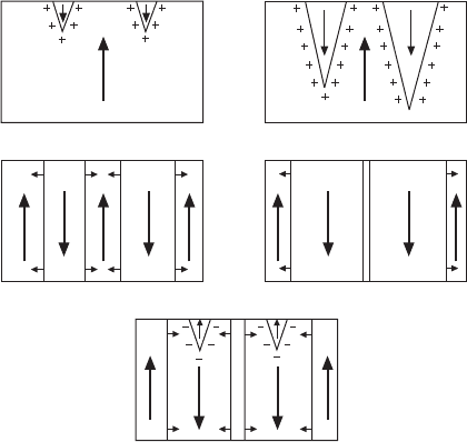
Nano- and micro-domain engineering 625
be completely single domain or it contains a large quantity of nanoscale
irremovable residual domains (Shur, 1996). In the latter case the nucleation
stage represents a transition of the invisible residual nano-domains into visible
ones as a result of the field-induced domain growth.
In high-quality crystals the appearance of new domains is observed as a
rule at the surface (Fig. 21.1a). The intrinsic surface dielectric gap existing
in any ferroelectric capacitor provokes incomplete compensation of the
depolarization field in the vicinity of the electrodes (Janovec, 1959; Shur,
1996). This residual field can provide the existence of residual ‘shallow’
domains and also facilitates the ‘nucleation’ process at the surface.
The second stage, ‘forward growth’ (domain tip propagation), represents
a fast expansion of the formed ‘nuclei’ in the polar direction. The tip of the
needle-like domain with charged domain walls rapidly moves through the
sample (Fig. 21.1b). The direct observation of this short stage encounters
experimental difficulties. That is the reason why this process is poorly
explored. The method used to study this stage consists of partial switching
by application of short pulses. It allows us to obtain and to study in detail the
stable structure with charged domain walls consisting of needle-like domains
which have not reached the opposite polar surface (Shur et al., 2000b). The
depolarization fields produced by bound charges result in pronounced optical
contrast due to electro-optical effect. The formation of the quasi-regular
cogged ‘charged domain wall’ and its expansion have been visualized in the
(a) (b)
(d)(c)
(e)
21.1
The main stages of the polarization reversal in ferroelectrics.
WPNL2204
Handbook of dielectric, piezoelectric and ferroelectric materials626
bulk of LN under continuous switching using the uniform metal electrodes
(Shur et al., 2000b).
The third stage, ‘sideways domain growth’ (spreading), is best studied
experimentally by direct in situ methods of domain observation with high
time resolution due to the remarkable optical contrast of the regions in the
vicinity of the domain walls. At this stage the domain growth is achieved
through the domain expansion in the direction transversal to the polar one
(Fig. 21.1c). It has been shown experimentally that under ‘equilibrium’
switching conditions (see Section 21.6) the essential anisotropy of the sideways
domain wall motion results in the growth of regular-shaped polygon domains
with sides oriented along preferred crystallographic directions (Fatuzzo and
Merz, 1967). The detailed study of this stage reveals that the domain shape
depends crucially on the switching conditions (Shur, 2005a, 2006). The
variation of the field pulse parameters and modification of the dielectric gap
properties allow the domain shape to be governed and various regular
and irregular shapes to be obtained (Shur et al., 1984b, 1985, 2002b; Shur,
2006).
The fourth stage, ‘coalescence of residual domains’ (merging), is observed
when the switching process is close to the completion (Fig 21.1d). At this
stage the pronounced deceleration of the approaching walls is observed. The
walls’ motion stops and after definite rest-time the residual domains between
these walls disappear very rapidly. This process leads to the jump-like switching
behavior, which can be one of the sources of the switching current
noise (Barkhausen noise) (Miller, 1960; Lines and Glass, 1977; Shur et al.,
2002a).
The fifth stage, ‘spontaneous backswitching’ (flip-back), represents partial
revival of the initial domain state after the electric field switch off. This
stage is poorly studied experimentally. Nevertheless, the role of this stage
during cyclic switching is crucial. The backswitching represents the enlargement
of the residual domains by the backward wall motion and the nucleation of
the domains with the initial orientation of spontaneous polarization after
abrupt decrease of the switching field (Fig. 21.1e). It is necessary to point
out that the backswitching stage occurs under the action of the abnormally
high field. That is the reason why various self-assembled nano-domain
structures can be produced (Shur et al., 2000a).
It must be understood that the different stages of the domain structure
evolution can occur simultaneously in different parts of a real ferroelectric
sample even during switching in uniform electric field. Moreover, during the
given switching experiment it can happen that not all the stages discussed
can be realized. For example, such stages as nucleation and forward growth
(Fig. 21.1a,b) are not realized for switching from the multidomain initial
state.
WPNL2204
Nano- and micro-domain engineering 627
21.3 Materials and experimental conditions
21.3.1 LN and LT family: from congruent to
stoichiometric
In this chapter the main attention will be paid to experimental study of the
single crystals of LN and LT family owing, first of all, to practical reasons.
LN and LT are the favourite materials of domain engineering. The production
of periodically poled nonlinear chips for light conversion based on these
materials opens wide possibilities for further upgrading of quasi-phase matching
devices.
Moreover, LN and LT have recently become the recognized leaders in the
study of the domain structure stimulated by practical reasons. It is possible
to claim that now LN and LT can be used also as model crystals for the study
of the domain kinetics as they possess the simplest domain structure and
permit in situ optical domain visualization.
LN and LT are uniaxial crystals with C
3V
(R
3c
) symmetry in ferroelectric
phase, thus possessing the domain structure with 180° domain walls only.
The direct study of the domain kinetics in LN and LT is due to optical
contrast of the domain walls. The origin of the contrast is the essential
change of the refractive index in the vicinity of the domain walls induced by
incompletely compensated depolarization field in materials with a pronounced
electro-optical effect.
In the most popular congruent compositions of LN (CLN) and LT (CLT)
the coercive field is enormously high and attains 210kV/cm. Thus, the
application of the necessary threshold field to the sample is coupled with
great experimental difficulty. For this reason both materials were named as
‘frozen ferroelectrics’ for many years. Recently, new representatives of LN
and LT family closer to stoichiometric composition have become available
for research and application (Furukawa et al., 1998; Kitamura et al., 1998;
Niwa et al., 2000; Huang et al., 2001). The stoichiometric LN (SLN) and LT
(SLT) demonstrate essentially lower values of the coercive field and
substantially different domain kinetics as compared with the congruent ones
(Kitamura et al., 1998; Niwa et al., 2000). In addition, we have studied
domain kinetics in LN and LT doped by MgO in order to increase essentially
the optical damage threshold, which is crucial for production of the periodical
poled elements for high-energy light conversion.
The LN and LT single crystals of congruent composition were grown
from the melt by the Czochralski method. The double-crucible modification
of this method and top-seeded solution growth method allows the production
of the near-stoichiometric LN and LT (Kitamura et al., 1998; Niwa et al.,
2000; Huang et al., 2001). Switching experiments were carried out in optical-
grade single-domain wafers cut perpendicular to the polar axis. The typical
thickness of the studied wafers ranges from 0.2 to 0.5mm for CLN and CLT
WPNL2204
Handbook of dielectric, piezoelectric and ferroelectric materials628
and from 1 to 2 mm for SLN and SLT. The polar surfaces of all studied
samples were carefully polished.
For in situ study of the domain kinetics in a uniform field we prepared
two types of circular transparent electrodes: (1) liquid electrolyte (water
solution of LiCl or pipe water) in a special fixture and (2) In
2
O
3
:Sn (ITO)
films deposited by magnetron sputtering, with diameter down to 1 mm. The
visualization by polarizing microscopy in transmitted and reflected light
with simultaneous TV-recording and subsequent image processing was used
for detailed study of the domain kinetics.
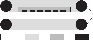
The LN and LT wafers, used for the periodical poling, were lithographically
patterned with periodic stripe NiCr or Al electrodes deposited on Z+-surface
only and oriented along one of Y-directions. The patterned surface was covered
by a photoresist layer about 1µm thick. A high voltage pulse producing an
electric field greater than the coercive one was applied to the structure through
the fixture containing the liquid electrolyte (Fig. 21.2). To observe the domain
patterns after partial poling both polar surfaces were etched with pure
hydrofluoric (HF) acid at room temperature. The surface relief obtained was
visualized by optical microscopy, scanning electron microscopy (SEM), and
various modes of scanning probe microscopy (SPM).
21.3.2 Relaxors
Relaxor ferroelectrics are among the most intensively studied materials due
to their unique properties which are useful for various important applications
(Cross, 1994; Blinc et al., 2006; Bokov and Ye, 2006a). They are included in
our investigations for the practical reasons resulting from prominent
electromechanical properties (Cross, 1994). Of course the domain kinetics in
these materials is far from the ‘model’ one because of their complicated
structure.
We have studied the hot-pressed high-density transparent lanthanum-doped
lead zirconate–titanate ceramics (Pb
1–x
La
x
)(Zr
0.65
Ti
0.35
)O
3
PLZT (5-12)/65/
35, which exhibits a classic relaxor behavior within a broad temperature
range. The plate thickness varied from 90 to 300µm. Two types of electrodes
5
–4–3–2–1
21.2
Experimental setup used for periodical poling: 1 wafer, 2 liquid
electrolyte, 3 insulating layer, 4 periodic electrodes, 5 O-rings.
WPNL2204
Nano- and micro-domain engineering 629
were used: (1) transparent ITO deposited by magnetron sputtering and (2)
gold deposited by thermal evaporation.
The hysteresis loops were measured under the action of ac triangular field
pulses in the frequency range from 0.02 to 0.2Hz and the field amplitude up
to 10 kV/cm. The switching charge has been obtained by digital integration
of the recorded switching current. The frequency range was chosen to provide
the ‘quasi-static switching regime’. The switching under the action of the
series of rectangular unipolar pulses with rise time about 20µs, amplitude up
to 10kV/cm and duration ranging from 50µs to 5s was carried out. The
pulse frequency was chosen sufficiently low to provide the complete
backswitching between subsequent pulses which results in good reproducibility
of the current data. All experiments have been done in temperature range
from 20 to 200°C.
Piezo-response force microscopy (PFM) mode was realized on the basis
of EXPLORER™ AFM. Conductive Co-coated silicon cantilevers with 75kHz
resonance frequency were used for visualization of domain patterns. The ac
modulation voltage with amplitude 10V and frequency 17kHz was applied
between the bottom electrode and the conductive tip being in contact with
the surface. Local mechanical deformation at the frequency of the reference
signal was induced by applied ac voltage due to reversed piezoelectric effect.
The piezoelectric response was detected by analyzing the scanning probe
microscopy (SPM) photodetector signal using the lock-in amplifier. The
phase of recorded signal differed by 180° for domains with opposite polarization
directions. The main PFM advantage is the ability to obtain the domain
contrast even in the case of complete screening of the depolarization field at
the surface.
21.3.3 Experimental methods of domain observation in
LN and LT: from optics to SPM
The number of different techniques ranging from common optical microscopy
to more sophisticated SPM has been widely used for the investigation of the
static domain patterns and the kinetics of the domain structure in LN and LT
family crystals. We shall only briefly discuss the most important visualization
techniques. A review of modern experimental methods has been published
(Soergel, 2005).
Selective chemical etching is one of the oldest and most popular techniques
used for revealing the domain structure in ferroelectrics. The inherent difference
in the etch rate for domains with opposite directions of spontaneous polarization
leads to the formation of steps on the polished sample’s surface at the position
of the domain walls. It has been revealed in LN and LT that the etching rates
for the faces of anti-parallel domains are drastically different. The Z-face
etches hundreds of times faster than Z+ one. This method is commonly used
WPNL2204