Zuo-Guang. Ye Advanced Dielectric Piezoelectric and Ferroelectric Materials: Synthesis, Characterisation and Applications
Подождите немного. Документ загружается.

Handbook of dielectric, piezoelectric and ferroelectric materials630
for precise measurement of the period and duty cycle of the engineered
periodic domain patterns in LN and LT using (HF) acid-based etchants (Ohnishi
and Iizuki, 1975; Alekseeva et al., 1986; Mizuuchi and Yamamoto, 1992;
Sones et al., 2002). The observation of revealed domain pattern can be
carried out by optical or scanning electron microscopy (SEM). Moreover,
the etch relief can be measured with high spatial resolution by the topographic
mode of SPM. Nevertheless, the interpretation of obtained images must be
done with care, because the etching relief for nanoscale domains can be
essentially different from the domain pattern due to strong anisotropy of
etching rate in the Y direction.
It is generally accepted that the etching procedure does not significantly
affect the domain structure. Thus, the etched relief structure must correlate
one-to-one with the existing stable domain pattern. It has been demonstrated
recently that this statement is not always true (Shur et al., 2005c). It has been
shown experimentally using SPM measurements that in MgO-doped
stoichiometric LT (MgO:SLT) crystals, contrary to current opinion, the domain
walls can be shifted considerably (about tenths of micrometers) from their
initial positions during etching. It has been found that the wall motion proceeded
even after the termination of the etching procedure. It has been revealed that
the whole consequence of the domain wall positions during etching is recorded
in the etching relief height and can be extracted with high spatial and temporal
resolution (Shur et al., 2005c). The main drawback of the etching technique
is that it is a destructive method, which is useless for in situ study of the
domain kinetics, and gives information only about the surface domain structure.
The SPM methods can be used for visualization of the static domain
patterns with nanoscale resolution even without preliminary etching. PFM
analyzes the piezoelectric response of the volume fraction mechanically
deforming under the locally applied ac electric field. Since any ferroelectric
is piezoelectric, it is possible to obtain a two-dimensional (2D) map of the
complete 3D piezoelectric tensor, which gives insight to the different
ferroelectric domain structures. In the case of investigated LN and LT possessing
the simple domain structure with 180° walls only the scanning of the polar
face allows one to distinguish the domains with opposite polarization sign
by recording the phase of the signal. The domain walls can be visualized by
recording the signal amplitude.
The widely accessible optical methods which present the unique possibility
of in situ observation of domain evolution using polarizing microscope are
the most informative and suitable (Burfoot and Taylor, 1979). These methods
are non-invasive, if the properly chosen intensity and wavelength of illumination
do not affect the domain kinetics. Even super-fast switching can be investigated
by using pulse lighting and high-speed photography (Malozemoff and
Slonczewski, 1979; O’Dell, 1981). The time resolution is determined by the
light pulse duration and can be above 10ns. The domains separated by 90°
WPNL2204
Nano- and micro-domain engineering 631
walls can be easily distinguished by polarizing microscopy due to the different
values of spontaneous birefringence (Blattner et al., 1948; Matthias and
Hippel, 1948). This effect has been used to study many ferroelectrics. But it
is unusable for antiparallel domains with 180° walls because of the identity
of optical indicatrix in neighboring domains. Some special techniques have
been developed for optical visualization of such domains.
In BaTiO
3
antiparallel domains become optically distinguished when the
electric field (Little, 1955; Merz, 1956) or corresponding mechanical forces
(Hooton and Meiz, 1955) are applied perpendicularly to the polar axis. The
rotation of the optical axis in opposite directions in different domains leads
to a difference between extinction positions of antiparallel domains, allowing
their visualization.
Miller and Savage (1959) and Savage and Miller (1960) have shown that
the antiparallel domains in BaTiO
3
can be observed in transmitted polarized
light during polarization reversal in a longitudinal field. Kobayashi et al. (1963)
showed that in this case domains are distinguishable only under the illumination
directed at small angles to the polar axis and explained this effect by the
existence of strain-induced birefringence in the vicinity of domain walls.
The linear electro-optic effect is the versatile property making possible
optical visualization of domains and/or domain boundaries. In the case of
anti-parallel 180° domains the electric field applied along the optical axis
induces the difference in refractive indices in Z+ and Z–domains. In LN and
LT the perturbation of the refractive index in the area near the domain walls
is induced by extremely high internal bias field. This effect allows the domains
to be visualized using polarized and phase contrast modes of the optical
microscopy. This also presents the unique opportunity of visualizing the
domains with charged domain walls embedded in the bulk. The drawback of
the optical methods imposed by the diffraction limiting the spatial resolution
to 0.5µm is outweighed by the ability to realize a high temporal resolution.
A promising new integral optical technique is based on the physical
phenomenon of light deflection at the domain boundaries. In these experiments,
a partially deflected laser beam produces, in the far-field, the light pattern
which carries information about the orientation of the domain walls. In LN
the light pattern is a six-point star, because in this material the individual
domains are mainly hexagons. The same experiments carried out in LT
demonstrate a three-point star pattern, because the observed domain shapes
are usually triangles. This method can be used for the statistical characterization
of the wall orientation in complicated multidomain patterns.
21.4 General consideration
In this chapter all stages of the domain structure evolution will be considered
from a unified point of view as a manifestation of the various nucleation
WPNL2204
Handbook of dielectric, piezoelectric and ferroelectric materials632
processes. This commonly accepted approach was proposed and developed
by Fatuzzo and Merz (1967) and Miller and Weinreich (1960). The nucleation
and growth approach is widely used for the description of the kinetics of
aggregative state changes during first-order phase transformation, e.g.
crystallization and melting (Shur, 2005). In our case the coexisting domains
with different orientation of the spontaneous polarization are considered as
an analogue of volumes occupied by different phases, while the domain
walls represent the phase boundaries. It has been shown by direct experiments
that the width of ferroelectric walls is a few unit cells (Lin and Bursill, 1982;
Bursill and Lin, 1986). This result supports the consideration of the domain
structure evolution as a discrete nucleation process. Following this approach
the domain kinetics during all the above-mentioned stages has to be considered
as a result of numerous elementary processes of thermally activated generation
of nuclei with a preferred orientation of the spontaneous polarization.
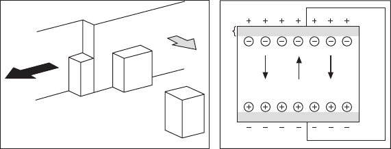
21.4.1 The elementary nucleation processes
The domain kinetics, similar to any first-order phase transformation kinetics,
is achieved through competitive formation of nuclei of three different
dimensionalities (Fig. 21.3). Each nucleus represents the nanoscale domain
with changed orientation of the spontaneous polarization.
The appearance of the optically observed new domains (‘nucleation of
new domains’) is a result of the expansion of either newly formed or residual
3D nanoscale nuclei. Such ‘invisible expansion’ occurs by 1D- and 2D-
nucleation (Fig. 21.3). In the real systems the heterogeneous nucleation
takes place during first-order phase transformation, and the position of the
nucleation sites is determined by imperfections and point defects. The
predominance of the nucleation at the sample surface is the special feature of
ferroelectrics caused by the existence of the intrinsic surface dielectric gap
playing the role of the ‘defect plane’.
1D
2D
3D
(a) (b)
L
ε
L
ε
P
s
E
dep
E
scr
21.3
Schemes: (a) of the nucleation processes of various
dimensionalities, (b) of the ferroelectric with intrinsic dielectric
surface layer.
WPNL2204
Nano- and micro-domain engineering 633
The growth of visible domains by motion of the walls (‘sideways domain
growth’) is achieved through 1D- and 2D-nucleation, as shown in Fig. 21.3.
The elementary steps with the thickness about one unit cell are generated by
2D-nucleation at the wall. The subsequent motion of the steps along the wall
is a result of 1D-nucleation. The crystal symmetry imposed the restrictions
on the orientation of the elementary steps thus leads to experimentally observed
anisotropy of the domain growth. The shape of isolated domains usually
observed during ‘equilibrium’ switching conditions is defined by the crystal
symmetry: e.g. square domains are formed in tetragonal phase of BaTiO
3
(Iona and Shirane, 1962) and hexagonal domains – in LN (C
3
or R
3c
symmetry)
(Prokhorov and Kuzminov, 1990).
The nucleation probability determines the rates of all switching processes.
For any first-order phase transformation it is determined by the driving
force value. The electric field averaged over the volume of the order of the
nucleus size (named in the following as ‘local field’, E
loc
) plays the role of
the driving force of nucleation during polarization reversal in ferroelectrics
(Shur, 1996). E
loc
is macroscopic electric field obeying macroscopic
electrodynamics equations with proper boundary conditions (Lifshitz et al.,
1985). E
loc
is essentially spatially inhomogeneous and changes during
polarization reversal. It is necessary to point out that E
loc
has nothing in
common with the local field which is analyzed while discussing the interaction
of the crystal lattice ions.
E
loc
in a ferroelectric capacitor is the sum of: (1) the external field applied
by electrode pattern, (2) the depolarization field produced by bound charges
developing as a result of spatial inhomogeneity of the spontaneous polarization
in multidomain state, (3) the external screening field originating from the
redistribution of the charges at the electrodes, and (4) the bulk screening
field governed by various bulk screening processes.
The external field is determined by the shape, sizes, and period of the
electrode pattern. The field singularities in the surface layer at the electrode
edges due to the fringe effect play the crucial role in the nucleation of the
new domains. The switching process usually starts through formation of the
nuclei at the electrode edge or at the tips of the stripe electrodes. Due to the
fringe effect the real value of E
loc
initiating the switching process in single-
domain state (threshold field) essentially exceeds the field value calculated
as potential difference divided by sample thickness. The pronounced field
concentration in the vicinity of the ends and corners of the stripe electrodes
must be accounted for while creating the tailored domain structures (Shur,
2005).
The depolarization field E
dep
is produced by bound charges existing at the
polar surfaces of the sample and at the charged walls of the encountering
domains (‘head to head’ or ‘tail to tail’). The bound charges density (ρ
b
) is
determined by spontaneous polarization (P
s
) by the following equation:
WPNL2204
Handbook of dielectric, piezoelectric and ferroelectric materials634
ρ
b
= – div P
s
21.1
For single-domain plate of typical ferroelectrics the depolarization field strength
can reach 10
8
V/m. It is clear that E
dep
far exceeding the experimentally
observed threshold or coercive fields leads to break-up of the single domain
state and fragmentation of the domain structure into narrow domains of
opposite sign.
In the volume of the isolated domain of ellipsoid shape:
E
dep
= L P
S
/εε
o
21.2
where L is the depolarization factor, which is essentially reduced for the
elongated domains. Thus, the wedge and needle-like shapes are the most
favorable for new domains due to minimization of the depolarization energy.
The domain growth by nucleation at the existing domain wall is determined
by the value of E
dep
at the wall front in the interface between the dielectric
gap and the ‘ferroelectric bulk’. This field is essentially spatially inhomogeneous
and strongly depends on the distance from the wall (Drougard and Landauer,
1959). For the sideways domain growth stage E
dep
increases with domain
enlargement, thus decreasing the nucleation probability at the moving wall.
This effect leads to experimentally observed deceleration and termination of
the wall motion (Drougard and Landauer, 1959; Shur, 1996, 2005a).
The effect of E
dep
is reduced by screening processes. For effective screening
of E
dep
the complete switching can be achieved even in a comparatively low
electric field. Only a small shift of the existing domain walls is observed for
ineffective screening due to the screening retardation. The incomplete screening
of E
dep
is the main source of the spontaneous backswitching (‘flip back’)
representing the partial recovering of the initial domain state after the external
field switch off. Two types of screening processes must be distinguished:
external and bulk.
External screening in ferroelectric capacitors is due to redistribution of
charges in the electrodes (the current in external circuit). The screening rate
is determined by the characteristic time of the external circuit τ
ex
(product of
effective resistance and capacity). Usually τ
ex
ranges from a few nanoseconds
to microseconds. The external screening field E
scr
(r,t) effectively compensates
E
dep
(r,t) thus allowing the long-distance-shift of the domain wall and drastically
diminishes the value of the applied external field E
ex
(r), which is necessary
for the complete switching. The experimentally observed switching time t
s
always exceeds τ
ex
as the complete switching can be obtained only if the
depolarization field is sufficiently screened.
The fast external screening never completely compensates E
dep
due to the
existence of the intrinsic dielectric surface layer (‘dielectric gap’ or ‘dead
layer’), in which spontaneous polarization is absent (Fig. 21.3b) (Fridkin,
1980; Shur, 1996).
WPNL2204
Nano- and micro-domain engineering 635
For a ferroelectric capacitor of thickness d the bulk residual depolarization
field E
rd
remains in the area freshly switched from one single-domain state
to another one even after complete external screening due to existence of the
intrinsic surface dielectric layer of the thickness L (Fridkin, 1980; Shur,
1996):
E
rd
= E
dep
– E
scr
= 2L/d [P
S
/(ε
L
ε
o
)] 21.3
where ε
L
is the dielectric permittivity of the surface dielectric gap.
E
rd
is several orders of magnitude less than E
dep
, but it is of the order of
the experimentally observed threshold/coercive fields. Thus, the effective
compensation of E
rd
by comparatively slow bulk screening processes is
necessary for complete switching. That is why bulk screening plays an essential
role in the evolution of the domain structure.
Bulk screening is the only way to compensate E
rd
existing after completion
of the external screening. Three groups of the bulk screening mechanisms
are usually considered: (1) redistribution of the bulk charges (Fridkin, 1980;
Shur, 1996), (2) reorientation of the defect dipoles (Lambeck and Jonker,
1986), (3) injection of carriers from the electrode through the dielectric gap
(Tagantsev et al., 2001). All bulk screening mechanisms are considerably
slower than the external ones, with typical time constants τ
b
ranging from
milliseconds up to days and even months.
According to the above-discussed considerations the local electric field
being the driving force of all nucleation processes is spatially inhomogeneous
and time dependent. After completion of the external screening the local
electric field at the given point and at the given moment E
loc
(r,t) is the sum
of the external field E
ex
(r), the residual depolarization field E
rd
(r,t), and bulk
screening field E
b
(r,t) (Shur, 1996, 1998; Shur and Rumyantsev, 1997 Shur):
E
loc
(r,t) = E
ex
(r) + E
rd
(r,t) + E
b
(r,t) 21.4
That is why the application of the short field pulse, for which the bulk
screening of the new state lags behind, is absolutely ineffective for the
creation of a modified domain pattern. The cooperative action of E
rd
and E
b
remaining after the external field is switched off leads to the spontaneous
backswitching process. This effect could be observed in the areas where the
value of E
loc
(r,t) exceeds the threshold field for the switching process E
th
,
i.e.:
E
loc
(r,t) = –[E
dep
(r,t) – E
scr
(r,t) + E
b
(r,t)] = – [E
rd
(r,t) + E
b
(r,t)] > E
th
21.5
The initial domain state can even be completely reconstructed for ineffective
screening of the modified E
dep
produced by the domain pattern formed at the
end of the electric field pulse. The conservation of the new domain configuration
can be realized only when the duration of the external field pulse is long
WPNL2204
Handbook of dielectric, piezoelectric and ferroelectric materials636
enough for effective bulk screening. Thus for an appropriate duration of the
field application it is possible to stabilize almost any domain pattern.
The systematic study of the polarization reversal in various ferroelectric
single crystals reveals a great variety of the domain kinetics scenarios. The
main problem in their classification lies in the fact that it is impossible to
attribute the given scenario to a definite range of applied fields and switching
rates. The critical values of the fields and rates corresponding to a replacement
of one domain kinetics scenario by another differ drastically for different
materials and experimental conditions.
Basing on the above-discussed approach we have chosen the ratio between
switching rate (1/t
s
) and bulk screening rate (1/τ
scr
) for quantitative
characterization of the screening efficiency. This parameter is named screening
effectiveness R (Shur, 2005, 2006(a)):
R = τ
scr
/t
s
21.6
Three ranges for screening effectiveness must be distinguished: (1) R << 1
– ‘complete screening’, (2) R ~ 1 – ‘incomplete screening’ and (3) R >> 1 –
‘ineffective screening’. It was confirmed both experimentally and by computer
simulation that the proposed ranges correspond to qualitatively different
switching regimes (scenarios of domain kinetics).
The complete screening corresponds to quasi-equilibrium switching
conditions when the reconstruction of the subsystem of the bulk screening
charges is fast enough to keep pace with the changes of the domain structure.
The retardation of the bulk screening makes the switching conditions non-
equilibrium. Thus the equilibrium switching conditions corresponds to R
<< 1 and the highly non-equilibrium ones to R >> 1.
Sideways domain wall motion is a result of step generation (2D nucleation)
and subsequent step growth (1D nucleation) along the wall (Fig. 21.3a). The
shape and orientation of the moving wall strongly depend on the spatial
distribution of the nucleation sites. Two limiting variants can be considered:
stochastic and predetermined.
Stochastic nucleation with random position of the nucleation sites at the
wall is the classical approach to the problem of the wall motion (Miller and
Weinreich, 1960b; Hayashi, 1972). This approach assumes that the switching
field is homogeneous and the step generation probability is independent of
the position at the wall. As a result, the shape of the moving wall becomes
irregular. In this case the deceleration of the wall by local pinning centers is
ineffective. The wall easily flows around the pinning center, because the
decrease of the nucleation probability occurs only in the vicinity of the
center, while the rest of the wall continues to move. The shape of individual
domains under stochastic nucleation is usually irregular and does not follow
the crystal symmetry.
However, in many ferroelectrics switched under usual experimental
conditions the domains demonstrate regular shape with walls strictly oriented
WPNL2204
Nano- and micro-domain engineering 637
along definite crystallographic directions. In LN the domains demonstrate
hexagon shape with walls strictly oriented along Y crystallographic directions.
This behavior can be understood, if we assume that the predetermined
nucleation prevails.
Predetermined nucleation means that the generation of the steps (2D-
nucleation) along the wall is spatially inhomogeneous. The preferred nucleation
at the given sites determined by field singularities can be produced both
artificially and during growth of isolated domain.
For growth of isolated domain the switching field at the wall is decreased
due to incomplete screening of the depolarization field. For a polygon domain
shape this screening retardation leads to formation of the field singularities
at the vertices leading to local increase of the step generation probability. In
this case the predetermined nucleation at polygon vertices must be realized.
The position of the nucleation sites for hexagon domains in LN is shown in
the Fig. 21.4. The crystal symmetry imposes restrictions on the directions of
the growth of the elementary steps, thus leading to anisotropy of the domain
growth, which is observed experimentally (Shur, 2005). In LN crystal with
C
3V
(R
3c
) symmetry the step propagation along three allowed directions
must prevail. The direct experimental observation of the domain kinetics
allows us to state that the steps propagate along the Y direction only (Shur,
2005, 2006). The steps generated at three Y non-adjacent vertices are growing
while the growth of the steps generated at three other vertices is completely
suppressed. The experimentally observed hexagon shape is obtained when
the step growth rate exceeds essentially the step generation rate.
The growth of the hexagon domain governed by predetermined nucleation
is demonstrated on the schematic drawing presented in Fig. 21.4. It is clearly
seen that the growing conditions for steps generated at the vertices A and B
are essentially different. The growth probability for steps generated at vertex
A must far exceed the probability at B, because the growth of the latter must
occur in the directions opposite to the preferable ones.
Y
Y
(a) (b)
A
B
A
B
A
B
AB
A
B
A
B
21.4
Predetermined nucleation: (a) step generation at vertices and (b)
step growth in three
Y
directions.
WPNL2204
Handbook of dielectric, piezoelectric and ferroelectric materials638
Within this consideration we have shown by computer simulation that the
growing domain preserves its polygon shape, if the step generation probability
at the faces is neglected (Lobov et al., 2006). The additional experimental
evidence of the proposed approach was obtained while observing the
propagation of macro-steps along the wall in three Y directions only. These
micrometer-scale steps formed as a result of interaction of the moving wall
with the crystal defects can be easily visualized in situ by optical microscopy
(Shur, 2005, 2006).
21.4.2 Artificially produced nucleation sites
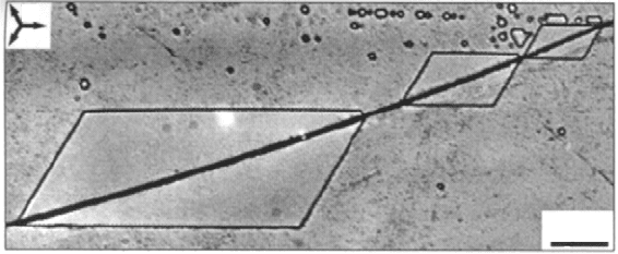
It is interesting to study the role of the predetermined nucleation on the
domain shape when the nucleation sites are produced artificially. The scratching
of the crystal polar surface is one of the possible ways to initiate the nucleation
in the given place. In this case the predetermined position of the nucleation
sites is caused by an artificial array of field concentrators produced by the
scratch. The slow switching using the solid liquid electrode of the sample
with a single scratch oriented along X axis produces the regular tetragons
(Fig. 21.5). It is clearly seen that the walls are strictly oriented along the Y
directions. Such behavior is an unequivocal experimental confirmation of
the prevailing role of the predetermined nucleation in LN.
21.5 Domain growth: from quasi-equilibrium to
highly non-equilibrium
21.5.1 Growth of isolated domains
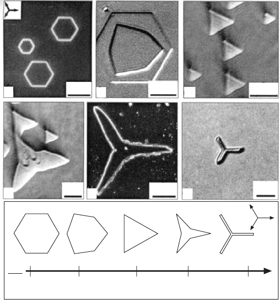
It has been shown that the shape of individual domains in LN essentially
depends on experimental conditions and can differ from the above-discussed
Y
30 µm
21.5
Tetragon domains in CLN. Predetermined nucleation initiated by
scratch oriented in
X
direction. Optical images of domains revealed
by etching.
WPNL2204
Nano- and micro-domain engineering 639
regular hexagon (Fig. 21.6). According to the mechanism of predetermined
nucleation it is possible to explain all shapes observed in LN and LT in wide
range of experimental conditions as a result of variation of the ratio between
rates of step generation and step growth. It is convenient to characterize the
step generation rate by experimentally measured vertex motion velocity V
gen
,
and the step growth – by motion velocity of the step edge V
gr
. The hexagon
shape is obtained, if condition V
gen
<< V
gr
is fulfilled.
It has been shown that the ratio between V
gen
and V
gr
is the main parameter
which governs the shape of isolated domain. The simulation of the domain
growth for wide range of V
gen
/V
gr
values allows us to obtain the smooth
variation of the domain shapes from equilateral hexagon to stars with three
rays (Fig. 21.6f).
Y
5 µm
(a)
(b)
5 µm
(c)
5 µm
(d) (e)
(f)
5 µm
10 µm
5 µm
Y
(g)
V
gen
V
gr
0 0.5 1 10 ∞
21.6
The domain shapes obtained as a result of switching in various
conditions in CLN: (a) hexagons, (b) irregular hexagon, (c), (d)
triangles, (d), (e) Mercedes stars, (f) star with three rays. Optical
images of domains revealed by etching. (a), (e) – dark field mode. (g)
Simulated dependence of domain shapes in LN on the ratio of step
generation to step growth rates.
WPNL2204