Bhushan B. Handbook of Micro/Nano Tribology, Second Edition
Подождите немного. Документ загружается.


© 1999 by CRC Press LLC
Yasutake, K., Umeno, M., and Kawabe, H. (1982b), “Compression Tests of Heat-Treated Czochralski-
Grown Silicon Crystals,” Phys. Status Solidi (a) 69, 333.
Yonenaga, I. and Sumino, K. (1978), “Dislocation Dynamics in the Plastic Deformation of Silicon
Crystals,” Phys. Status Solidi (a) 50, 685.
Yonenaga, I. and Sumino, K. (1984), “Role of Carbon in the Strengthening of Silicon Crystals,” Jpn.
J. Appl. Phys. 23, L590.
Zhang, L.M., Uttamchandari, D., and Culshaw, B. (1991), “Measurement of the Mechanical Properties
of Silicon Microresonators,” Sensors Actuators, A29, 79.
Zhang, X., Zohar, Y., and Zhang, T.Y. (1997), “Measurements of Residual Stresses in Low-Stress Silicon
Nitride Thin Films Using Micro-Rotating Structures,” Mater. Res. Soc. Symp. Proc. 444, 111–116.
Bhushan, B. “Micro/Nanotribology and Micro/Nanomechanics of MEMS...”
Handbook of Micro/Nanotribology.
Ed. Bharat Bhushan
Boca Raton: CRC Press LLC, 1999

© 1999 by CRC Press LLC
16
Micro/Nanotribology
and
Micro/Nanomechanics
of MEMS Devices
Bharat Bhushan
16.1 Introduction
Background • Tribological Issues
16.2 Experimental Techniques
Description of Apparatus and Test Procedures • Test Samples
16.3 Results and Discussion
Micro/Nanotribological Studies of Virgin, Coated, and Treated
Silicon Samples • Micro/Nanotribological Studies of Doped
and Undoped Polysilicon Films, SiC Films, and Their
Comparison to Single-Crystal Silicon • Macroscale
Tribological Studies of Virgin, Coated, and Treated Samples •
Boundary Lubrication Studies • Component Level Studies
16.4 Closure
References
16.1 Introduction
16.1.1 Background
The advances in silicon photolithographic process technology since 1960s have led to the development
of microcomponents or microdevices, known as microelectromechanical systems (MEMS). More
recently, lithographic processes have been developed to process nonsilicon materials. These lithographic
processes are being complemented with nonlithographic micromachining processes for fabrication of
milliscale components or devices. Using these fabrication processes, researchers have fabricated a wide
variety of miniaturized devices, such as acceleration, pressure and chemical sensors, linear and rotary
actuators, electric motors, gear trains, gas turbines, nozzles, pumps, fluid valves, switches, grippers,
tweezers, and optoelectronic devices with dimensions in the range of a couple to a few thousand microns
(for an early review, see Peterson, 1982; for recent reviews, see Muller et al., 1990; Madou, 1997; Trimmer,
1997; and Bhushan, 1998a). MEMS technology is still in its infancy and the emphasis to date has been
on the fabrication and laboratory demonstration of individual components. MEMS devices have begun

© 1999 by CRC Press LLC
to be commercially used, particularly in the automotive industry. Silicon-based high-
g
acceleration
sensors are used in airbag deployment (Bryzek et al., 1994). Acceleration sensor technology is slightly
less than a billion-dollar-a-year industry dominated by Lucas NovaSensor and Analog Devices. Texas
Instruments uses deformable mirror arrays on microflexures as part of airline-ticket laser printers and
high-resolution projection devices.
Potential applications of MEMS devices include silicon-based acceleration sensors for anti-skid braking
systems and four-wheel drives, silicon-based pressure sensors for monitoring pressure of cylinders in
automotive engines and of automotive tires, and various sensors, actuators, motors, pumps, and switches
in medical instrumentation, cockpit instrumentation, and many hydraulic, pneumatic, and other con-
sumer products (Fujimasa, 1996). MEMS devices are also being pursued in magnetic storage systems
(Bhushan, 1996a), where they are being developed for supercompact and ultrahigh-recording-density
magnetic disk drives. Horizontal thin-film heads with a single-crystal silicon substrate, referred to as
silicon planar head (SPH) sliders are mass-produced using integrated-circuit technology (Lazarri and
Deroux-Dauphin, 1989; Bhushan et al., 1992). Several integrated head/suspension microdevices have
been fabricated for contact recording applications (Hamilton, 1991; Ohwe et al., 1993). High-bandwidth
servo-controlled microactuators have been fabricated for ultrahigh-track-density applications which
serve as the fine-position control element of a two-stage, coarse/fine servo system, coupled with a
conventional actuator (Miu and Tai, 1995; Fan et al., 1995b). Millimeter-sized wobble motors and actu-
ators for tip-based recording schemes have also been fabricated (Fan and Woodman, 1995a). In some
cases, MEMS devices are used primarily for their miniature size, while in others, as in the case of the air
bags, because of their high reliability and low-cost manufacturing techniques. This latter fact has been
possible since semiconductor-processing costs have reduced drastically over the last decade, allowing the
use of MEMS in many previously impractical fields.
The fabrication techniques for MEMS devices employ photolithography and fall into three basic
categories: bulk micromachining, surface micromachining, and LIGA a German acronym (Lithographie
Galvanoformung Abformung) for lithography, electroforming, and plastic molding. The first two
approaches, bulk and surface micromachining, use planar photolithographic fabrication processes devel-
oped for semiconductor devices in producing two-dimensional (2D) structures (Jaeger, 1988; Madou,
1997; Bhushan, 1998a). Bulk micromachining employs anisotropic etching to remove sections through
the thickness of a single-crystal silicon wafer, typically 250 to 500 µm thick. Bulk micromachining is a
proven high-volume production process and is routinely used to fabricate microstructures such as
acceleration and pressure sensors and magnetic head sliders. Surface micromachining is based on depos-
iting and etching structural and sacrificial films to produce a free-standing structure. These films are
typically made of low-pressure chemical vapor deposition (LPCVD) polysilicon film with 2 to 20 µm
thickness. Surface micromachining is used to produce surprisingly complex micromechanical devices
such as motors, gears, and grippers. LIGA is used to produce high-aspect ratio (HAR) MEMS devices
that are up to 1 mm in height and only a few microns in width or length (Becker et al., 1986). The LIGA
process yields very sturdy 3D structures due to their increased thickness. The LIGA process is based on
the combined use of X-ray photolithography, electroforming, and molding processes. One of the limi-
tations of silicon microfabrication processes originally used for fabrication of MEMS devices is lack of
suitable materials which can be processed. With LIGA, a variety of nonsilicon materials such as metals,
ceramics and polymers can be processed. Nonlithographic micromachining processes, primarily in
Europe and Japan, are also being used for fabrication of millimeter-scale devices using direct material
microcutting or micromechanical machining (such as micromilling, microdrilling, microturning) or
removal by energy beams (such as microspark erosion, focused ion beam, laser ablation, and machining,
and laser polymerization) (Friedrich and Warrington, 1998; Madou, 1998). Hybrid technologies including
LIGA and high-precision micromachining techniques have been used to produce miniaturized motors,
gears, actuators, and connectors (Lehr et al., 1996, 1997; Michel and Ehrfeld, 1998). These millimeter-
scale devices may find more immediate applications.

© 1999 by CRC Press LLC
Silicon-based MEMS devices lack high-temperature capabilities with respect to both mechanical and
electrical properties. Recently, researchers have been pursuing SiC as a material for high-temperature
microsensor and microactuator applications (Tong et al., 1992; Shor et al., 1993). SiC is a likely candidate
for such applications since it has long been used in high-temperature electronics, high-frequency and
high-power devices, such as SiC metal–semiconductor field effect transistors (MESFETS) (Spencer et al.,
1994) and inversion-mode metal-oxide-semiconductor field effect transistors (MOSFETS). Many other
SiC devices have also been fabricated including ultraviolet detectors, SiC memories, and SiC/Si solar cells.
SiC has also been used in microstructures such as speaker diaphragms and X-ray masks. For a summary
of SiC devices and applications, see Harris (1995). Table 16.1 compares selected bulk properties of SiC
and Si(100). Because of the large band gap of SiC, almost all devices fabricated from SiC have good high-
temperature properties. This high-temperature capability of SiC combined with its excellent mechanical
properties, thermal dissipative characteristics, chemical inertness, and optical transparency makes SiC
an ideal choice for complementing polysilicon (polysilicon melts at 1400°C) in MEMS devices. Since
MEMS devices need to be of low cost to be viable in most applications, researchers have found low-cost
techniques of producing single-crystal 3C-SiC (cubic or
β
-SiC) films via epitaxial growth on large area
silicon substrates (Zorman et al., 1995). This technique allows high-volume batch processing and has the
advantage of having silicon as the substrate, an inexpensive material for which microfabrication and
micromachining technologies are well established. It is believed that these films will be well suited for
MEMS devices.
16.1.2 Tribological Issues
In MEMS devices, various forces associated with the device scale down with the size. When the length
of the machine decreases from 1 mm to 1 µm, the area decreases by a factor of a million and the volume
decreases by a factor of a billion. The resistive forces such as friction, viscous drag, and surface tension
that are proportional to the area, increase a thousand times more than the forces proportional to the
volume, such as inertial and electromagnetic forces. The increase in resistive forces leads to tribological
concerns, which become critical because friction/stiction (static friction), wear and surface contamination
affect device performance and in some cases, can even prevent devices from working.
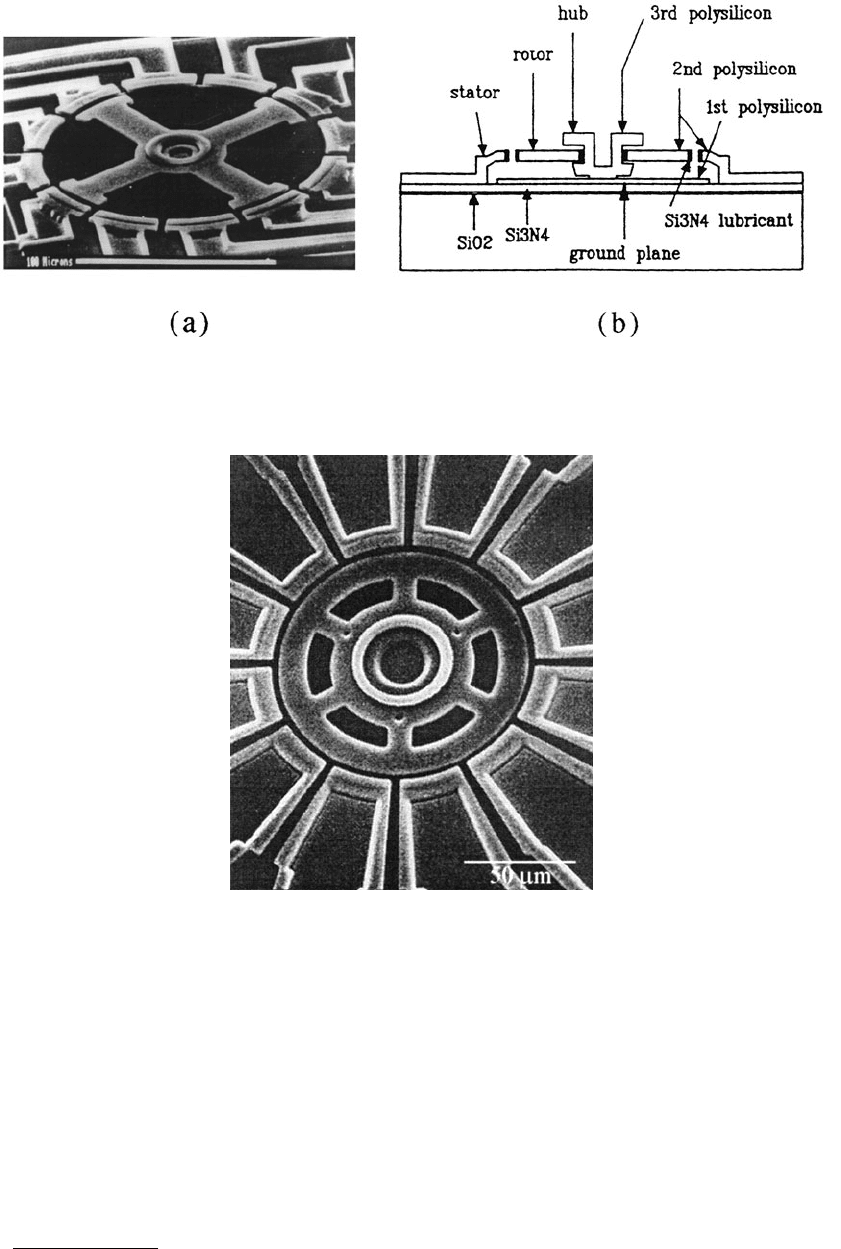
Examples of two micromotors using polysilicon as the structural material in surface micro-
machining — a variable capacitance side drive and a wobble (harmonic) side drive — are shown in
Figures 16.1 and 16.2, which can rotate up to 100,000 rpm. Microfabricated variable-capacitance side-
drive micromotor with 12 stators and a 4-pole rotor shown in Figure 16.1 is produced using a three-
layer polysilicon process and the rotor diameter is 120 µm and the air gap between the rotor and stator
is 2 µm (Tai et al., 1989). It is driven electrostatically to continuous rotation (by electrostatic attraction
between positively and negatively charged surfaces). The intermittent contact at the rotor–stator interface
and physical contact at the rotor–hub flange interface result in wear issues, and high stiction between
the contacting surfaces limits the repeatability of operation or may even prevent the operation altogether.
Figure 16.2 shows the SEM micrograph of a microfabricated harmonic side-drive (wobble) micromotor
TABLE 16.1
Selected Bulk Properties
a
of 3C (
β
- or cubic) SiC and Si(100)
Sample
Density
(kg/m
3
)
Hardness
(GPa)
Elastic
Modulus
(GPa)
Fracture
Toughness
(MPa m
1/2
)
Thermal
Conductivity
b
(W/m K)
Coeff. of
Thermal
Expansion
b
(
×
10
–6
/°C)
Melting
Point (°C)
Band-Gap
(eV)
β
–SiC 3210 23.5–26.5 440 4.6 85–260 4.5–6 2830 2.3
Si(100) 2330 9–10 130 0.95 155 2–4.5 1410 1.1
a
Unless stated otherwise, data shown were obtained from Bhushan and Gupta (1997).
b
Obtained from Shackelford et al. (1994).
© 1999 by CRC Press LLC
(Mehregany et al., 1988). In this motor, the rotor wobbles around the center bearing post rather than
the outer stator. Again friction/stiction and wear of rotor-center bearing interface are of concern. There
is a need for development of bearing/bushing materials that are both compatible with MEMS fabrication
processes and which provide superior friction and wear performance. Monolayer lubricant films are also
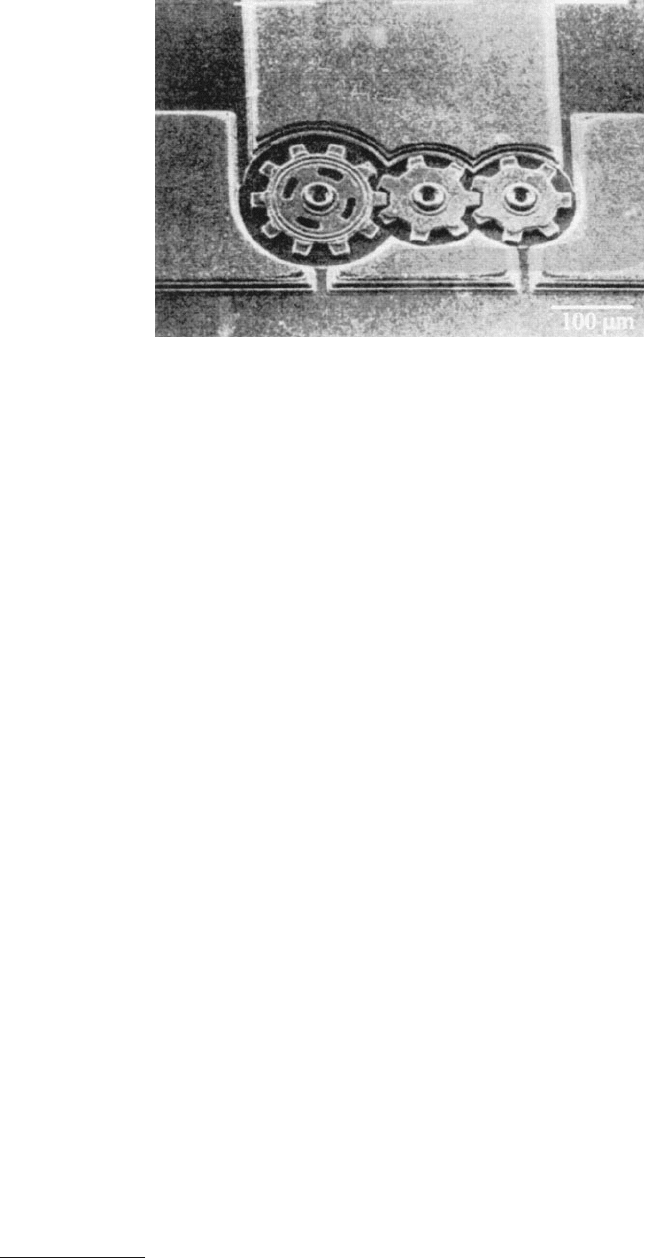
of interest. Figure 16.3 shows the SEM micrograph of an air turbine with gear or blade rotors, 125 to
240 µm in diameter, fabricated using polysilicon as the structural material in surface micromachining.
The two flow channels on the top are connected to the two independent input ports and the two flow
channels at the bottom are connected to the output port. Wear at the contact of gear teeth is a concern.
In microvalves used for flow control, the mating valve surfaces should be smooth enough to seal while
FIGURE 16.1
(a) SEM micrograph, and (b) schematic cross-section of a variable capacitance side-drive micromotor
fabricated of polysilicon film. (From Tai et al., 1989,
Sensors Actuators
A21–23, 180–83. With permission.)
FIGURE 16.2
SEM micrograph of a harmonic side-drive (wobble) micromotor. (From Mehregany, M. et al., 1990,
in
Proc. IEEE Micro Electromechanical Systems,
pp. 1–8, IEEE, New York. With permission.)
© 1999 by CRC Press LLC
maintaining a minimum roughness to ensure low friction/stiction (Bhushan, 1996a, 1998b). Studies have
been conducted to measure the friction/stiction in micromotors (Tai and Muller, 1990), gear systems
(Gabriel et al., 1990) and polysilicon microstructures (Lim et al., 1990) to understand friction mechanisms.
Several studies have been conducted to develop solid and liquid lubricant and hard films to minimize
friction and wear (Bhushan et al., 1995b; Deng et al., 1995; Beerschwinger et al., 1995; Koinkar and
Bhushan, 1996a,b; Bhushan, 1996b; Henck, 1997).
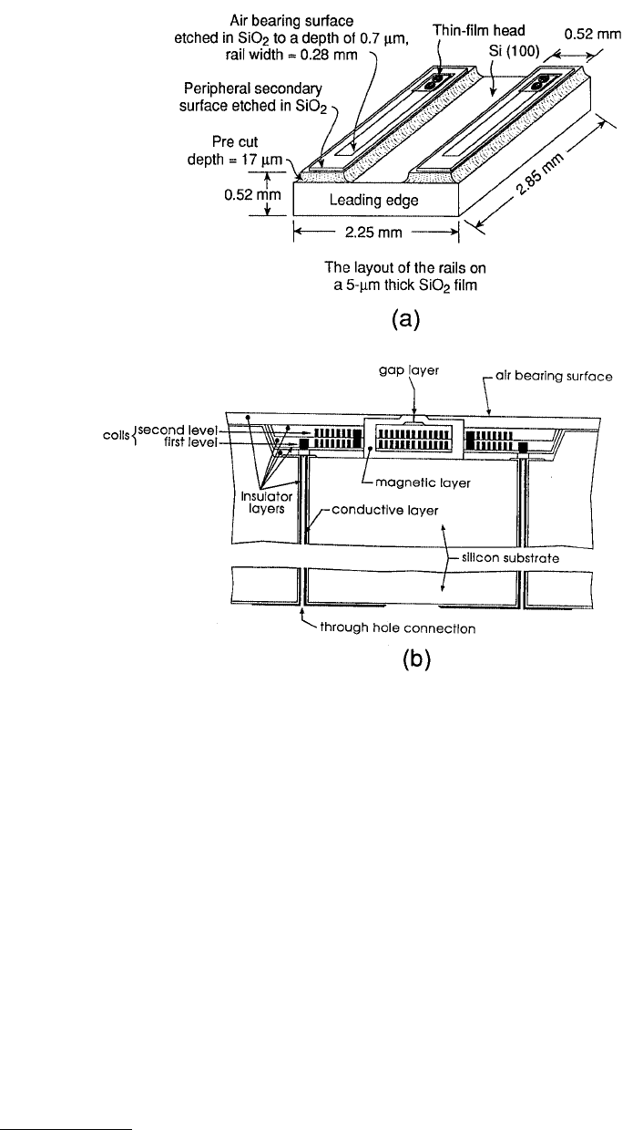
In a silicon planar head slider for magnetic disk drives shown in Figure 16.4, wear and friction/stiction
are an issue because of the close proximity between the slider and disk surfaces during steady operation
and continuous contacts during start and stops (Lazzari and Deroux-Dauphin, 1989; Bhushan et al.,
1992). Hard diamondlike carbon (DLC) coatings are used as an overcoat for protection against corrosion
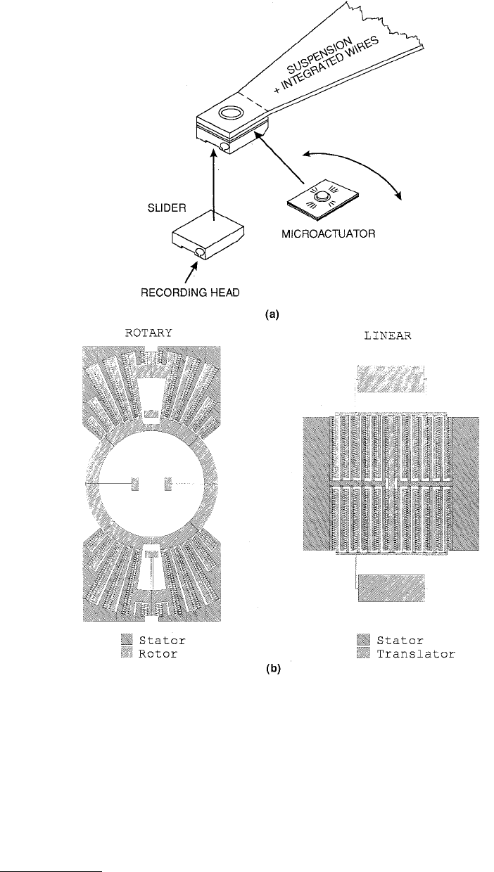
and wear. Two electrostatically driven rotary and linear microactuaters (surface-micromachined, poly-
silicon microstructure) for a magnetic disk drive shown in Figure 16.5, consist of a movable plate
connected only by springs to a substrate, on which there are two sets of mating interdigitated electrodes
which activate motion of the plate in opposing directions. Any unintended contacts may result in wear
and stiction.
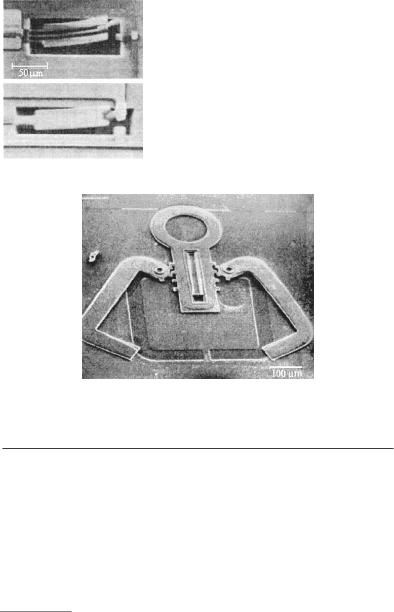
Figure 16.6 shows an SEM micrograph of a micromechanical switch (Peterson, 1979). As the voltage
is applied between the deflection electrode and the p
+
ground plane, the cantilever beam is deflected and
the switch closes, connecting the contact electrode and the fixed electrode; wear during contact is of
concern. Figure 16.7 shows an SEM micrograph of a pair of tongs (Mehregany et al., 1988). The jaws
open when the linearly sliding handle is pushed forward, demonstrating the linear slide and the linear-
to-rotary motion conversion; for this pair of tongs, the jaws open up to 400 µm in width. Wear at the
teeth is of concern.
As an example of nonsilicon components, Figure 16.8a shows a DC brushless permanent magnet
millimotor (diameter = 1.9 mm, length = 5.5 mm) with an integrated milligear box which is produced
with parts obtained by hybrid fabrication processes including the LIGA process, micromechanical
machining, and microspark erosion techniques (Lehr et al., 1996, 1997; Michel and Ehrfeld, 1998). The
motor can rotate up to 100,000 rpm and deliver a maximum torque of 7.5 µNm. The rotor, supported
on two ruby bearings, consists of a tiny steel shaft and a diametrically magnetized rare earth magnet.
The rotational speed of the motor can be converted by the use of a milligear box to increase the torque
for a specific application. Gears are made of metal (e.g., electroplated Ni–Fe) or injected polymer materials
(e.g., POM) using the LIGA process, Figures 16.8b and c. Optimum materials and liquid and solid
lubrication approaches for bearings and gears are needed.
FIGURE 16.3
SEM micrograph of a gear train with three meshed gears, in an air turbine. (From Mehregany, M.
et al., 1988,
IEEE Trans. Electron Devices
35, 719–723. With permission.)
© 1999 by CRC Press LLC
There are tribological issues in the fabrication processes as well. For example, in surface microma-
chining, the suspended structures can sometimes collapse and permanently adhere to the underlying
substrate, Figure 16.9 (Guckel and Burns, 1989). The mechanism of such adhesion phenomena needs to
be understood (Mastrangelo, 1997).
Friction/stiction and wear clearly limit the lifetimes and compromise the performance and reliability
of microdevices. Since microdevices are designed to small tolerances, environmental factors, surface
contamination, and environmental debris affect their reliability. There is a need for development of a
fundamental understanding of friction/stiction, wear, and the role of surface contamination and envi-
ronment in microdevices (Bhushan, 1998a). A few studies have been conducted on the tribology of bulk
silicon and polysilicon films used in microdevices (Bhushan and Venkatesan, 1993a,b; Gupta et al., 1993;
Venkatesan and Bhushan, 1993, 1994; Gupta and Bhushan, 1994; Bhushan and Koinkar, 1994; Bhushan,
1996b). Mechanical properties of polysilicon films are not well characterized (Mehregany et al., 1987;
Ericson and Schweitz, 1990; Schweitz, 1991; Guckel et al., 1992; Bhushan, 1995; Fang and Wickert, 1995).
The advent of atomic force/friction force microscopy (AFM/FFM) (Bhushan, 1995, 1997; Bhushan et al.,
1995a) has allowed the study of surface topography, adhesion, friction, wear, lubrication, and measure-
ment of mechanical properties, all on a micro- to nanometer scale. Recently, microtribological studies
FIGURE 16.4
Schematic (a) of a silicon planar head slider and (b) of cross section of the slider for magnetic disk
drive applications. (From Bhushan, B. et al., 1992,
IEEE Trans Magn.
28, 2874–2876. With permission.)
© 1999 by CRC Press LLC
have been conducted using the AFM/FFM on undoped and doped silicon and polysilicon films and SiC
films that are used in MEMS devices (Bhushan, 1996b, 1997, 1998; Bhushan et al., 1994, 1997a,b, 1998;
Li and Bhushan, 1998; Sundararajan and Bhushan, 1998).
This chapter presents a review of macro- and micro/nanotribological studies of single-crystal silicon
and polysilicon, oxidized and implanted silicon, doped and undoped polysilicon films and SiC films. A
summary of limited component-level tests is also presented.
FIGURE 16.5
Schematics of (a) a microactuator in place with magnetic head slider, and (b) top view of two
electrostatic, rotary and linear microactuators (electrode tree structure). (From Fan, L.S. et al., 1995;
IEEE Trans. Ind.
Electron.
42, 222–233. With permission.)
© 1999 by CRC Press LLC
16.2 Experimental Techniques
16.2.1 Description of Apparatus and Test Procedures
16.2.1.1 Micro/Nanoscale Tests
A modified AFM/FFM (Nanoscope III, Digital Instruments, Santa Barbara, CA), was used for the
micro/nanotribological studies. Surface roughness and microscale friction measurements were simulta-
neously made over a scan size of 10
×
10 µm with an Si
3
N
4
tip (tip radius ~ 50 nm, cantilever stiffness
~ 0.6 N/m) sliding over the sample surface orthogonal to the long axis of the cantilever at 25 µm/s. A
coefficient of friction and conversion factors for converting the friction signal voltage to force units (nN)
were obtained through the methods developed previously by Bhushan and co-workers (Bhushan, 1995).
The normal loads used in the friction measurements varied between 50 to 300 nN. The reported values
are each an average of six separate measurements.
FIGURE 16.6
SEM micrograph of single-contact and double-con-
tact (with two orientations of the fixed electrodes) designs of micro-
mechanical switches (Peterson, 1979). (From Peterson, K.E., 1979,
IBM J. Res. Dev.
23, 376. With permission.)
FIGURE 16.7
SEM micrograph of a partially released pair of tongs. (From Mehregany, M. et al., 1988,
IEEE Trans.
Electron. Devices
35, 719–723. With permission.)